

■ Electrical Characteristics (Ta = 25˚C)
GaAs MMICs GN8061
GN8061
GaAs IC
For semiconductor laser drive
■ Features
●
High-speed switching
●
High output
●
Pulse current and DC bias current can be controlled.
■ Absolute Maximum Ratings (Ta = 25˚C)
Parameter
Power supply voltage
Pin voltage
Power current
Output current
Allowable power dissipation
Channel temperature
Storage temperature
Operating ambient temperature
Symbol
V
DD
V
SS
V
Ib1
* 1
V
Ib2
V
IN
V
Ip
* 5
V
OUT
* 1
I
DD
* 4
I
SS
I
OUT
P
D
* 2
T
ch
T
stg
T
opr
* 3
Rating
6
– 6
6
0.5
– 0.5 to V
DD
–1.5
1.5 to 6
6
55
40
225
700
150
– 55 to +150
–10 to + 75
Unit
V
V
V
V
V
V
V
mA
mA
mA
mW
˚C
˚C
˚C
Parameter
Pulse output current
Bias output current
Supply current
Input voltage
Rise time
Fall time
Test circuit
1
1
2
2
2
2
2
3
3
Condition
V
IN
= 2.0V, V
Ib2
= – 5V
V
IN
= 0.4V, V
Ib2
= – 5V
I
P
= 0, V
Ib1
= 5V, V
Ib2
= 0
I
P
= 0, V
Ib1
= 0, V
Ib2
= 0
I
P
= 0, V
Ib1
= 5V, V
Ib2
= – 5V
V
Ib1
= 5V, V
Ib2
= – 5V, VIN= 0.4V
I
P
= 0
V
Ib1
= 0, V
Ib2
– 5V, IP =100mA
Min
100
80
2.5
Typ
120
1
100
1
0.05
35
25
Max
5
5
0.1
55
40
0.4
7
5
Unit
mA
mA
mA
mA
mA
mA
mA
V
V
ns
ns
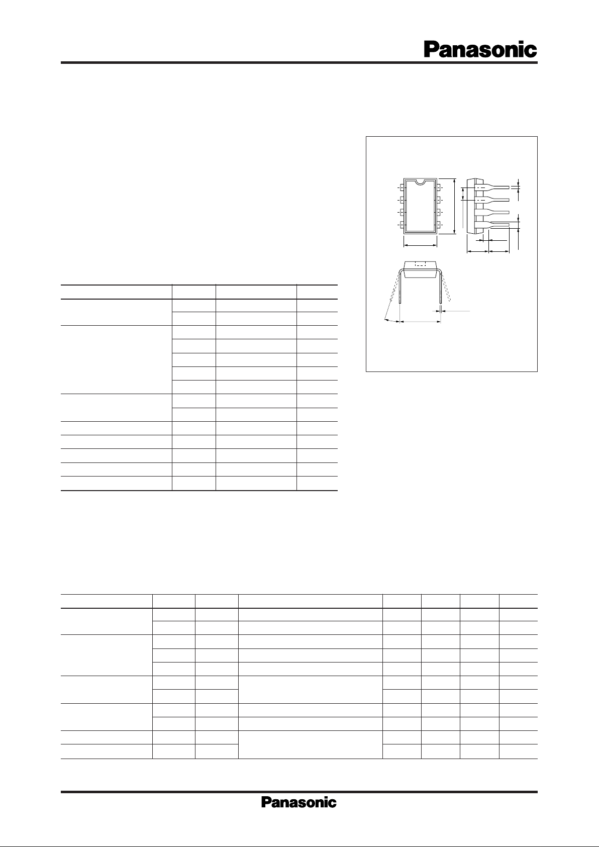
Unit : mm
1 : GND
2 : V
Ib1
3 : V
Ib2
4 : OUT
5 : V
IP
6 : V
DD
7 : V
IN
8 : V
SS
8-Lead Plastic DIL Package
* 1 Do not apply the voltage higher than the set VDD.
* 2 Guaranteed for the unit in the natural atmosphere.
* 3 IC circuit functioning range. Note however that the electrical characteristics shown
at Ta= 25˚C is not guaranteed.
* 4 IDD is a current when the pulse output current and bias output current are zero.
* 5 Voltage when the constant current source has been connected.
Symbol
I
pmax.
I
pmin.
I
bmax.
I
bmin. 1
I
bmin. 2
I
DD
* 1
I
SS
V
IH
V
IL
t
r
* 2
t
f
* 2
Note : Following condition is applied unless otherwise specified: VDD= 5V, VSS= – 5V, V
Ib1
= 0V, V
Ib2
= 0V
Set the supply current of constant current source to IP=120mA and load resistance to RL=10Ω
0.51.3typ.
4.0max.
0.7min.
4.5max.
0.35max.
6.4±0.2
7.62±0.2
2.54±0.25
10max.
0 to 15˚
1
2
3
4
8
7
6
5
10µS
2
µS
2.5V min.
0.4V max.
*
The rise/fall time of the input signal
is 2ns (10 to 90%)
Output waveform
Input signal
GaAs MMICs GN8061
* 1 The current value to be supplied from the 5V power supply is a total sum of this value plus the pulse output current and bias output current.
* 2 Waveform of input and output signals
Test circuit 1 Test circuit 2
Test circuit 3
C1 : 0.1µF
C2 : 3.3µF
C3 : 2200pF
R1 : 10Ω
R2 : 50Ω
V
IN
I
P
=120mA
–5V
–5V
1234
8765
0V
5V
C1 C2
–
+
C2
+
–
C2
R1
C1
+
–
5V
C1
A
0.4V
I
P
=0mA
–5V
V
Ib2
1234
8765
V
Ib1
5V
C1 C2
–
+
C2
+
–
C2
R1
C1
+
–
5V
C1
A
PULSE
GENERATOR
I
P
=100mA
–5V
–5V
1234
8765
5V
C1
C3
C3
C2
R2
–
+
C2
+
–
C2
R1
FET PROBE
C1
+
–
5V
C1
90%
t
f
t
r
10%
t
r ··· 10% to 90%
t
f ··· 90% to 10%
 Loading...