

Page 1

MICROCOMPUTER MN101C
MN101C77C/F77G
LSI User ’s Manual
Pub.No.21477-011E
Page 2

Page 3

PanaXSeries is a trademark of Matsushita Electric Industrial Co., Ltd.
The other corporation names, logotype and product names written in this book are trademarks or registered trademarks of their
corresponding corporations.
Request for your special attention and precautions in using the technical information
and semiconductors described in this book
(1) An export permit needs to be obtained from the competent authorities of the Japanese Government if any of
the products or technologies described in this book and controlled under the "Foreign Exchange and Foreign
Trade Law" is to be exported or taken out of Japan.
(2) The technical information described in this book is limited to showing representative characteristics and
applied circuits examples of the products. It neither warrants non-infringement of intellectual property right
or any other rights owned by our company or a third party, nor grants any license.
(3) W e are not liable for the infringement of rights owned by a third party arising out of the use of the product or
technologies as described in this book.
(4) The products described in this book are intended to be used for standard applications or general electronic
equipment (such as office equipment, communications equipment, measuring instrument s and household
appliances).
Consult our sales staff in advance for information on the following applications:
• Special applications (such as for airplanes, aerospace, automobiles, traffic control equipment, combustion
equipment, life support systems and safety devices) in which exceptional quality and reliability are required,
or if the failure or malfunction of the products may directly jeopardize life or harm the human body.
• Any applications other than the standard applications intended.
(5) The products and product specifications described in this book are subject to change without notice for
modification and/or improvement. At the final stage of your design, purchasing, or use of the prod ucts,
therefore, ask for the most up-to-date Product Standards in advance to make sure that the latest specifications
satisfy your requirements.
(6) When designing your equipment, comply with the guaranteed values, in particular those of maximum rating,
the range of operating power supply volta ge, and heat radiation characteristics. Otherwise, we will not be
liable for any defect which may arise later in your equipment.
Even when the products are used within the guaranteed values, take into the consideration of incidence of
break down and failure mode, possible to occur to semiconductor products. Measures on the systems such as
redundant design, arresting the spread of fire or preventing glitch are recommended in order to prevent
physical injury, fire, social damages, for example, by using the products.
(7) When using products for which damp-proof packing is required, observe the conditions (including shelf life
and amount of time let standing of unsealed items) agreed upon when specification sheets are individually
exchanged.
(8) This book may be not reprinted or reproduced whether wholly or partially, without the prior written
permission of Matsushita Electric Industrial Co., Ltd.
If you have any inquiries or questions about this book or our semiconductors, please contact one of our sales
offices listed at the back of this book.
Page 4
About This Manual
Organization
In this LSI manual, this LSI functions are presented in the following order : overview, basic CPU functions, interrupt
functions, port functions, timer functions, serial functions, and other peripheral hardware functions.
Each section contains overview of function, block diagram, control register, operation, and setting example.
Manual Configuration
Each section of this manual consists of a title, summary, main text, key information, precautions and warnings, and
references.
The layout and definition of each section are shown below.
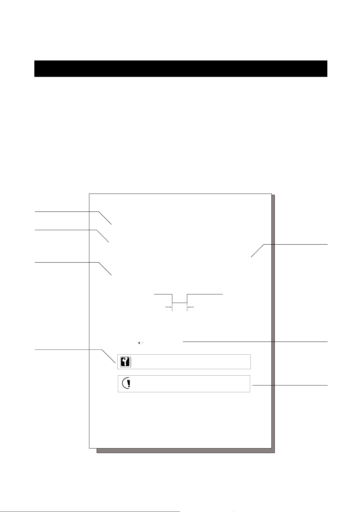
Subtitle
Sub-subtitle
The smallest block
in this manual.
Main text
Key information
Important information
from the text.
Chapter 2 Basic CPU
2-8 Reset
2-8-1 Reset operation
The CPU contents are reset and registers are initialized when the NRST pin (P.27) is pulled to low.
Initiating a Reset
There are two methods to initiate a reset.
(1) Drive the NRST pin low for at least four clock cycles.
NRST pin should be holded "low" for more than 4 clock cycles (200 nS at a 20 MHz).
NRST pin
4 clock cycles
(200 nS at a 20 MHz)
Figure 2-8-1 Minimum Reset Pulse Width
(2) Setting the P2OUT7 flag of the P2OUT register to "0" outputs low level at P27 (NRST) pin. And
transfering to reset by program (software reset) can be executed. If the internal LSI is reset and
register is initiated, the P2OUT7 flag becomes "1" and reset is released.
[ Chapter 4. 4-4-2 Registers ]
On this LSI, the starting mode is NORMAL mode that high oscillation is the base clock.
When the power voltage low circuit is connected to NRST pin, circuit that gives pulse for
enough low level time at sudeen unconnected. And reset can be generated even if its pulse
is low level as the oscillation clock is under 4 clocks, take notice of noise.
Summary
Introduction to the
section.
References
References for the
main text.
Precautions and
warnings
Precautions are listed
in case.
Be sure to read these
of lost functionality or
damage.
About This Manual 1
II - 44
Reset
Page 5

Finding Desired Information
This manual provides three methods for finding desired information quickly and easily.
(1) Consult the index at the front of the manual to locate the beginning of each section.
(2) Consult the table of contents at the front of the manual to locate desired titles.
(3) Chapter names are located at the top outer corner of each page, and section titles are located
at the bottom outer corner of each page.
Related Manuals
Note that the following related documents are available.
"MN101C Series LSI user's Manual"
<Describes the device hardware>
"MN101C Series Instruction Manual"
<Describes the instruction set.>
"MN101C Series C Compiler User's Manual: Usage Guide"
<Describes the installation, the commands, and options of the C Compiler.>
"MN101C Series C Compiler User's Manual: Language Description"
<Describes the syntax of the C Compiler.>
"MN101C Series C Compiler User's Manual: Library Reference"
<Describes the standard library of the C Compiler.>
"MN101C Series Cross-assembler User's Manual"
<Describes the assembler syntax and notation.>
"MN101C Series C Source Code Debugger User's Manual"
<Describes the use of C source code debugger.>
"MN101C Series PanaX Series Installation Manual"
<Describes the installation of C compiler, cross-assembler and C source code debugger
and the procedure for bringing up the in-circuit emulator.>
About This Manual 2
Page 6

Page 7

Chapter 1 Overview
1
Chapter 2 CPU Basics
Chapter 3 Interrupts
2
3
3
Chapter 4 I/O Ports
Chapter 5 Prescaler 5
Chapter 6 8-bit Timers
Chapter 7 16-bit Timer
Chapter 8 Time Base Timer /
8-bit Free-running Timer
4
6
7
8
11
2
Chapter 9 Watchdog Timer
Chapter 10 Buzzer
Chapter 11 Serial Interface 0,1
Chapter 12 Serial Interface 3
Chapter 13 Serial Interface 4
Chapter 14 Automatic Transfer
Controller
Chapter 15 A/D Converter
9
10
11
12
13
14
15
Chapter 16 D/A Converter
Chapter 17 Appendices
Chapter 18 Flash EEPROM
16
17
18
Page 8

Contents
Chapter 1 Overview
1-1 Overview ..................................................................................................................... I - 2
1-1-1 Overview .................................................................................................... I - 2
1-1-2 Product Summary ....................................................................................... I - 2
1-2 Hardware Functions .................................................................................................... I - 3
1-3 Pin Description............................................................................................................ I - 9
1-3-1 Pin Configuration ....................................................................................... I - 9
1-3-2 Pin Specification....................................................................................... I - 10
1-3-3 Pin Functions ........................................................................................... I - 1 1
1- 4 Block Diagram ........................................................................................................... I - 17
1-4-1 Block Diagram .......................................................................................... I - 1 7
1- 5 Electrical Characteristics ........................................................................................... I - 18
1-5-1 Absolute Maximum Ratings ..................................................................... I - 18
1-5-2 Operating Conditions ............................................................................... I - 19
1-5-3 DC Characteristics .................................................................................... I - 22
1-5-4 A/D Converter Characteristics ................................................................. I - 26
1-5-5 D/A Converter Characteristics ................................................................. I - 27
1-6 Precautions................................................................................................................ I - 28
1-6-1 General Usage .......................................................................................... I - 28
1-6-2 Unused Pins ............................................................................................. I - 2 9
1-6-3 Power Supply ........................................................................................... I - 31
1-6-4 Power Supply Circuit................................................................................ I - 32
1-7 Package Dimension ................................................................................................... I - 33
Chapter 2 CPU Basics
2-1 Overview.................................................................................................................. II - 2
2-1-1 Block Diagram ....................................................................................... II - 3
2-1-2 CPU Control Registers ........................................................................... II - 4
2-1-3 Instruction Execution Controller ........................................................... II - 5
2-1-4 Pipeline Process...................................................................................... II - 6
2-1-5 Registers for Address.............................................................................. II - 6
2-1-6 Registers for Data ................................................................................... II - 7
2-1-7 Processor Status Word ............................................................................ II - 8
2-1-8 Addressing Modes ............................................................................... II - 10
2-2 Memory Space....................................................................................................... II - 12
2-2-1 Memory Mode ...................................................................................... II - 12
2-2-2 Single-chip Mode ................................................................................. II - 13
2-2-3 Special Function Registers...................................................................... II - 14
2-3 Bus Interface ............................................................................................................ II - 15
ii
contents
Page 9

2-3-1 Bus Controller ......................................................................................... II - 15
2-3-2 Control Registers..................................................................................... II - 16
2-4 Standby Function..................................................................................................... II - 19
2-4-1 Overview ................................................................................................. II - 19
2-4-2 CPU Mode Control Register.................................................................... II - 2 1
2-4-3 Transition between SLOW and NORMAL.............................................. II - 22
2-4-4 Transition to ST ANDBY Modes ............................................................. II - 23
2- 5 Clock Switching........................................................................................................ II - 25
2-6 Bank Function .......................................................................................................... II - 27
2-6-1 Overview ................................................................................................. II - 27
2-6-2 Bank Setting ............................................................................................ II - 27
2-6-3 Bank Memory Space ............................................................................... II - 29
2- 7 ROM Correction ....................................................................................................... II - 30
2-7-1 Overview ................................................................................................. II - 30
2-7-2 Correction Sequence ............................................................................... II - 30
2-7-3 ROM Correction Control Register ........................................................... II - 32
2-7-4 ROM Correction Setup Example .............................................................. II - 35
2-8 Reset ........................................................................................................................ II - 38
2-8-1 Reset Operation....................................................................................... II - 38
2-8-2 Oscillation Stabilization W ait T ime.......................................................... II - 40
2-9 Register Protection................................................................................................... II - 42
2-9-1 Overview ................................................................................................. II - 42
2-9-2 Setting of the Register Protection Function ............................................ II - 4 2
2-9-3 Rewrite Procedure ................................................................................... II - 42
Chapter 3 Interrupts
3-1 Overview................................................................................................................. III - 2
3-1-1 Functions ............................................................................................... III - 3
3-1-2 Block Diagram ...................................................................................... III - 4
3-1-3 Operation ............................................................................................... III - 5
3-1-4 Interrupt Flag Setup............................................................................... III - 14
3-2 Control Registers.................................................................................................. III - 15
3-2-1 Registers List ....................................................................................... III - 15
3-2-2 Interrupt Control Registers.................................................................. III - 16
3-3 External Interrupts ................................................................................................... III - 38
3-3-1 Overview ................................................................................................ III - 38
3-3-2 Block Diagram ........................................................................................ III - 39
3-3-3 Control Registers.................................................................................... III - 42
3-3-4 Programmable Active Edge Interrupt ..................................................... III - 47
3-3-5 Both Edges Interrupt.............................................................................. III - 48
3-3-6 Key Input Interrupt ................................................................................ III - 19
3-3-7 Noise Filter ............................................................................................. III - 51
iii
contents
Page 10

3-3-8 AC Zero-Cross Detector ........................................................................ III - 54
Chapter 4 I/O Ports
4-1 Overview .................................................................................................................. IV - 2
4-1-1 I/O Port Diagram...................................................................................... IV - 2
4-1-2 I/O Port Status at Reset ........................................................................... IV - 3
4-1-3 Control Registers..................................................................................... IV - 4
4-2 Port 0 ........................................................................................................................ IV - 6
4-2-1 Description.............................................................................................. IV - 6
4-2-2 Registers ................................................................................................. IV - 7
4-2-3 Block Diagram ......................................................................................... IV - 8
4-3 Port 1 ....................................................................................................................... IV - 12
4-3-1 Description............................................................................................. IV - 12
4-3-2 Registers ................................................................................................ IV - 13
4-3-3 Block Diagram ........................................................................................ IV - 16
4-4 Port 2 ....................................................................................................................... IV - 17
4-4-1 Description............................................................................................. IV - 17
4-4-2 Registers ................................................................................................ IV - 18
4-4-3 Block Diagram ........................................................................................ IV - 19
4-5 Port 5 ....................................................................................................................... IV - 21
4-5-1 Description............................................................................................. IV - 21
4-5-2 Registers ................................................................................................ IV - 22
4-5-3 Block Diagram ........................................................................................ IV - 23
4-6 Port 6 ....................................................................................................................... IV - 26
4-6-1 Description............................................................................................. IV - 26
4-6-2 Registers ................................................................................................ IV - 27
4-6-3 Block Diagram ........................................................................................ IV - 29
4-7 Port 7 ....................................................................................................................... IV - 30
4-7-1 Description............................................................................................. IV - 30
4-7-2 Registers ................................................................................................ IV - 31
4-7-3 Block Diagram ........................................................................................ IV - 33
4-8 Port 8 ....................................................................................................................... IV - 37
4-8-1 Description............................................................................................. IV - 37
4-8-2 Registers ................................................................................................ IV - 38
4-8-3 Block Diagram ........................................................................................ IV - 40
4-9 Port A ...................................................................................................................... IV - 41
4-9-1 Description............................................................................................. IV - 41
4-9-2 Registers ................................................................................................ IV - 42
4-9-3 Block Diagram ........................................................................................ IV - 44
4-10 Real Time Output Control (Port 1) ........................................................................... IV - 45
iv
contents
Page 11

4-10-1 Registers ................................................................................................ IV - 45
4-10-2 Operation................................................................................................ IV - 46
4-11 Synchronous Output (Port 7) .................................................................................. IV - 4 8
4-11-1 Block Diagram ........................................................................................ IV - 48
4-11-2 Registers ................................................................................................ IV - 49
4-11-3 Operation................................................................................................ IV - 50
4-11-4 Setup Example ........................................................................................ IV - 52
Chapter 5 Prescaler
5-1 Overview .................................................................................................................... V - 2
5-1-1 Peripheral Functions ................................................................................. V - 3
5-1-2 Block Diagram ........................................................................................... V - 4
5-2 Control Registers........................................................................................................ V - 5
5-2-1 Registers List............................................................................................. V - 5
5-2-2 Control Registers....................................................................................... V - 6
5-3 Operation.................................................................................................................. V - 11
5-3-1 Operation................................................................................................. V - 11
5-3-2 Setup Example ......................................................................................... V - 12
Chapter 6 8-bit T imers
6-1 Overview................................................................................................................. VI - 2
6-1-1 Functions .................................................................................................VI - 2
6-1-2 Block Diagram ........................................................................................VI - 3
6-2 Control Registers...................................................................................................... VI - 6
6-2-1 Registers ................................................................................................. VI - 6
6-2-2 Programmable Timer Registers ................................................................ VI - 8
6-2-3 Timer Mode Registers ............................................................................ VI - 10
6- 3 8-bit Timer Count..................................................................................................... VI - 15
6-3-1 Operation................................................................................................ VI - 15
6-3-2 Setup Example ........................................................................................ VI - 17
6-4 8-bit Event Count .................................................................................................... VI - 19
6-4-1 Operation................................................................................................ VI - 19
6-4-2 Setup Example ........................................................................................ VI - 21
6-5 8-bit Timer Pulse Output ......................................................................................... VI - 23
6-5-1 Operation................................................................................................ VI - 23
6-5-2 Setup Example ........................................................................................ VI - 24
6-6 8-bit PWM Output .................................................................................................. VI - 26
6-6-1 Operation................................................................................................ VI - 26
6-6-2 Setup Example ........................................................................................ VI - 28
6-7 8-bit Timer Synchronous Output............................................................................. VI - 3 0
v
contents
Page 12

6-7-1 Operation................................................................................................ VI - 30
6-7-2 Setup Example ........................................................................................ VI - 31
6-8 Serial Interface Transfer Clock Output .................................................................... VI - 33
6-8-1 Operation................................................................................................ VI - 33
6-8-2 Setup Example ........................................................................................ VI - 34
6-9 Simple Pulse W idth Measurement........................................................................... VI - 36
6-9-1 Operation................................................................................................ VI - 36
6-9-2 Setup Example ........................................................................................ VI - 37
6-10 Cascade Connection ............................................................................................... VI - 3 9
6-10-1 Operation................................................................................................ VI - 39
6-10-2 Setup Example ........................................................................................ VI - 41
6-11 Remote Control Carrier Output ................................................................................ VI - 43
6-11-1 Operation................................................................................................ VI - 43
6-11-2 Setup Example ........................................................................................ VI - 44
Chapter 7 16-bit T imer
7-1 Overview................................................................................................................ VII - 2
7-1-1 Functions .............................................................................................. VII - 2
7-1-2 Block Diagram ..................................................................................... VII - 3
7-2 Control Registers................................................................................................... VII - 4
7-2-1 Registers ............................................................................................... VII - 4
7-2-2 Programmable Timer Registers............................................................ VII - 5
7-2-3 Timer Mode Registers.......................................................................... VII - 8
7-3 16-bit Timer Count .............................................................................................. VII - 10
7-3-1 Operation ............................................................................................ VII - 10
7-3-2 Setup Example.................................................................................... VII - 13
7-4 16-bit Event Count .............................................................................................. VII - 15
7-4-1 Operation ............................................................................................ VII - 15
7-4-2 Setup Example.................................................................................... VII - 17
7-5 16-bit Timer Pulse Output................................................................................... VII - 19
7-5-1 Operation ............................................................................................ VII - 19
7-5-2 Setup Example.................................................................................... VII - 21
7-6 16-bit Standard PWM Output
(Only duty can be changed consecutively) .................................... VII - 23
7-6-1 Operation ............................................................................................ VII - 23
7-6-2 Setup Example.................................................................................... VII - 25
7-7 16-bit High Precision PWM Output
(Cycle/Duty can be changed consecutively)...................................... VII - 27
7-7-1 Operation ............................................................................................ VII - 27
7-7-2 Setup Example.................................................................................... VII - 29
7-8 16-bit Timer Synchronous Output ...................................................................... VII - 31
vi
contents
Page 13

7-8-1 Operation ............................................................................................ VII - 31
7-8-2 Setup Example.................................................................................... VII - 32
7-9 16-bit Timer Capture ........................................................................................... VII - 34
7-9-1 Operation ............................................................................................ VII - 34
7-9-2 Setup Example.................................................................................... VII - 37
Chapter 8 Time Base Timer / 8-bit Free-running Timer
8-1 Overview ................................................................................................................ VIII - 2
8-1-1 Functions .............................................................................................. VIII - 2
8-1-2 Block Diagram ....................................................................................... VIII - 3
8-2 Control Registers.................................................................................................... VIII - 4
8-2-1 Control Registers................................................................................... VIII - 4
8-2-2 Programmable Timer Registers .............................................................. VIII - 5
8-2-3 Timer Mode Registers ........................................................................... VIII - 6
8- 3 8-bit Free-running Timer......................................................................................... VIII - 7
8-3-1 Operation............................................................................................... VIII - 7
8-3-2 Setup Example ..................................................................................... VIII - 10
8- 4 Time Base Timer ................................................................................................... VIII - 12
8-4-1 Operation............................................................................................. VIII - 12
8-4-2 Setup Example ..................................................................................... VIII - 14
Chapter 9 Watchdog Timer
9-1 Overview................................................................................................................. IX - 2
9-1-1 Block Diagram ...................................................................................... IX - 2
9-2 Control Registers.................................................................................................... IX - 3
9-3 Operation ................................................................................................................ IX - 4
9-3-1 Operation ............................................................................................... IX - 4
9-3-2 Setup Example....................................................................................... IX - 7
Chapter 10 Buzzer
10-1 Overview ................................................................................................................... X - 2
10-1-1 Block Diagram .......................................................................................... X - 2
10-2 Control Register ........................................................................................................ X - 3
10-3 Operation................................................................................................................... X - 4
10-3-1 Operation.................................................................................................. X - 4
10-3-2 Setup Example .......................................................................................... X - 5
Chapter 11 Serial Interface 0,1
vii
contents
Page 14

11-1 Overview .................................................................................................................. XI - 2
11-1-1 Functions ................................................................................................ XI - 2
11-1-2 Block Diagram ......................................................................................... XI - 4
11-2 Control Registers...................................................................................................... XI - 6
11-2-1 Registers ................................................................................................. XI - 6
11-2-2 Serial Interface 0 Data Buffer Registers ................................................... XI - 7
11-2-3 Serial Interface 0 Mode Registers............................................................ XI - 8
11-2-4 Serial Interface 1 Data Buffer Registers ................................................. XI - 14
11-2-5 Serial Interface 1 Mode Registers.......................................................... XI - 15
11-3 Operation................................................................................................................ XI - 21
11-3-1 Clock Synchronous Serial Interface ...................................................... XI - 21
11-3-2 Serial interface 0 Synchronous Serial Interface Pin Setup ..................... XI - 33
11-3-3 Serial interface 1 Synchronous Serial Interface Pin Setup ..................... XI - 36
11-3-4 Setup Example ....................................................................................... XI - 39
11-3-5 UART Serial Interface............................................................................ XI - 4 2
11-3-6 Serial interface 0 UART Serial Interface Pin Setup ................................ XI - 5 4
11-3-7 Serial interface 1 UART Serial Interface Pin Setup ................................ XI - 5 6
11-3-8 Setup Example ....................................................................................... XI - 58
Chapter 12 Serial Interface 3
12-1 Overview............................................................................................................... XII - 2
12-1-1 Functions ............................................................................................. XII - 2
12-1-2 Block Diagram .................................................................................... XII - 3
12-2 Control Registers .................................................................................................. XII - 4
12-2-1 Registers .............................................................................................. XII - 4
12-2-2 Data Buffer Registers .......................................................................... XII - 5
12-2-3 Mode Registers ...................................................................................... XII - 6
12-3 Operation............................................................................................................... XII - 10
12-3-1 Clock Synchronous Serial Interface ..................................................... XII - 10
12-3-2 Setup Example ...................................................................................... XII - 24
12-3-3 Single Master IIC Interface................................................................... XII - 27
12-3-4 Setup Example ...................................................................................... XII - 36
Chapter 13 Serial Interface 4
13-1 Overview ................................................................................................................ XIII - 2
13-1-1 Functions .............................................................................................. XIII - 2
viii
contents
Page 15

13-1-2 Block Diagram ....................................................................................... XIII - 3
13-2 Control Registers.................................................................................................... XIII - 4
13-2-1 Registers List......................................................................................... XIII - 4
13-2-2 Data Register......................................................................................... XIII - 5
13-2-3 Mode Registers ..................................................................................... XIII - 6
13-3 Operation................................................................................................................ XIII - 9
13-3-1 Setup Example of the Slave IIC Serial Interface ................................... XIII - 11
Chapter 14 Automatic Transfer Controller
14-1 Overview ................................................................................................................ XIV - 2
14-1-1 A TC1 ..................................................................................................... XIV - 2
14-1-2 Functions .............................................................................................. XIV - 3
14-1-3 Block Diagram ....................................................................................... XIV - 4
14-2 Control Registers.................................................................................................... XIV - 5
14-2-1 Registers ............................................................................................... XIV - 5
14-3 Operation................................................................................................................ XIV - 9
14-3-1 Basic Operations and Timing ................................................................ XIV - 9
14-3-2 Setting the Memory Address .............................................................. XIV - 11
14-3-3 Setting the Data Transfer Count ......................................................... XIV - 12
14-3-4 Setting the Data Transfer Modes ........................................................ XIV - 13
14-3-5 Transfer Mode 0.................................................................................. XIV - 14
14-3-6 Transfer Mode 1.................................................................................. XIV - 15
14-3-7 Transfer Mode 2.................................................................................. XIV - 16
14-3-8 Transfer Mode 3.................................................................................. XIV - 17
14-3-9 Transfer Mode 4.................................................................................. XIV - 18
14-3-10 Transfer Mode 5.................................................................................. XIV - 19
14-3-11 Transfer Mode 6.................................................................................. XIV - 20
14-3-12 Transfer Mode 7.................................................................................. XIV - 22
14-3-13 Transfer Mode 8.................................................................................. XIV - 24
14-3-14 Transfer Mode 9.................................................................................. XIV - 26
14-3-15 Transfer Mode A................................................................................. XIV - 28
14-3-16 Transfer Mode B ................................................................................. XIV - 29
14-3-17 Transfer Mode C ................................................................................. XIV - 30
14-3-18 Transfer Mode D ................................................................................. XIV - 31
14-3-19 Transfer Mode E ................................................................................. XIV - 32
14-3-20 Transfer Mode F ................................................................................. XIV - 33
14-4 Setup Example ...................................................................................................... XIV - 34
Chapter 15 A/D Converter
15-1 Overview ................................................................................................................. XV - 2
15-1-1 Functions ............................................................................................... XV - 2
ix
contents
Page 16

15-1-2 Block Diagram ........................................................................................ XV - 3
15-2 Control Registers..................................................................................................... XV - 4
15-2-1 Registers ................................................................................................ XV - 4
15-2-2 Control Registers.................................................................................... XV - 5
15-2-3 Data Buffers ........................................................................................... XV - 7
15-3 Operation................................................................................................................. XV - 8
15-3-1 Setup .................................................................................................... XV - 1 0
15-3-2 Setup Example ...................................................................................... XV - 12
15-3-3 Cautions ............................................................................................... XV - 16
Chapter 16 D/A Converter
16-1 Overview ................................................................................................................ XVI - 2
16-1-1 Functions .............................................................................................. XVI - 2
16-2 Operation................................................................................................................ XVI - 3
16-3 Control Registers.................................................................................................... XVI - 4
16-3-1 Overview ............................................................................................... XVI - 4
16-3-2 Control Registers................................................................................... XVI - 5
16-3-3 Input Data Register ............................................................................... XVI - 6
16-4 Setup Example ........................................................................................................ XVI - 7
Chapter 17 Appendices
17-1 Probe Switches ..................................................................................................... XVII - 2
17-1-1 PRB-MBB101C77-M.............................................................................. XVII - 2
17-1-2 PX-CN101-M ......................................................................................... XVII - 3
17-1-3 PX-ADP101-64-M.................................................................................. XVII - 4
17-1-4 PRB-DMY101C77-M ............................................................................. XVII - 5
17-2 Special Function Registers List ............................................................................ XVII - 6
17-3
Instruction Set..................................................................................................... XVII - 15
17-4
Instruction Map .................................................................................................. XVII - 21
Chapter 18 Flash EEPROM
18-1 Overview ............................................................................................................. XVIII - 2
18-1-1 Overview .............................................................................................. XVIII - 2
18-1-2 Differences between Mask ROM version and EPROM version........... XVIII - 4
18-2 Pin Descriptions .................................................................................................. XVIII - 5
18-3 Electrical Characteristics ..................................................................................... XVIII - 6
18-3-1 Absolute Maximum Ratings ................................................................. XVIII - 6
18-3-2 Operating Conditions ........................................................................... XVIII - 7
18-3-3 DC Characteristics ................................................................................ XVIII - 8
x
contents
Page 17

18-4 Reprogramming Flow........................................................................................... XVIII - 9
18-5 PROM writer mode ............................................................................................ XV III - 10
18-6 Onboard Serial Programming Mode .................................................................. XVII I - 1 2
18-6-1 Overview ............................................................................................ XVIII - 12
18-6-2 Circuit Requirements for the T arget Board (in Clock Synchronous
Communication using the YDC Serial Writer)..................................... XVIII - 13
18-6-3 Circuit Requirements for the T arget Board (in Clock Synchronous
Communication using the PanaX Serial Writer).................................. XVIII - 16
xi
contents
Page 18

Page 19

Chapter 1 Overview
1
Page 20

Chapter 1 Overview
1-1 Overview
1-1-1 Overview
The MN101C series of 8-bit single-chip microcontroller incorporates multiple types of peripheral functions.
This chip series is well suited for camera, VCR, MD, TV, CD, LD, printer, telephone, home automation
products, pager, air conditioner, PPC remote control, fax machine, musical instrument, and other applications.
The MN101C77 series brings to embedded microcontroller applications flexible, optimized hardware
configurations and a simple efficient instruction set. The MN101C77C has an internal 48 KB of ROM and
3 KB of RAM. Peripheral functions include 5 external interrupts, 17 internal interrupts including NMI,
independent 6 timer counters, 4 sets of serial interfaces, A/D converter, D/A converter, watchdog timer,
automatic data transfer, synchronous output, buzzer output, and remote control output. The configuration of this microcontroller is well suited for application such as a system controller in a camera, VCR
selection timer, CD player, or MD.
With two oscillation systems (max.20 MHz/32 kHz) contained on the chip, the system clock can be
switched to high speed oscillation (NORMAL mode), or to low speed oscillation (SLOW mode). The
system clock is generated by dividing the oscillation clock. The best operation clock for the system can
be selected by switching its frequency by software. There are 2 choices for high speed oscillation : the
normal mode, which has a system clock based on the clock (fosc/2) divided by 2, and the 2x-speed
mode, which has a system clock based on the same cycle clock (fosc).
On the normal mode, when the oscillation source(fosc) is 8 MHz, minimum instructions execution
time is for 250 ns, and when fosc is 20 MHz, it is 100 ns. On the 2x-speed mode, CPU is operated with
the same cycle to the external clock, when fosc is 8 MHz, minimum instructions execution time is 125 ns.
The packages are 64-pin LQFP and 64-pin TQFP (under development).
1-1-2 Product Summary
This manual describes the following models of the MN101C77 series. These products have same peripheral functions. (Refer to chapter 18 Flash EEPROM for Flash version.)
Table 1-1-1 Product Summary
Model ROM Size RAM Size Classification
MN101C77C 48 KB 3 KB Mask ROM version
MN101CF77G 128 KB 6 KB Flash EEPROM version
I - 2
Overview
Page 21

1-2 Hardware Functions
CPU Core MN101C Core
- LOAD-STORE architecture (3-stage pipeline)
- Half-byte instruction set / Handy addressing
- Memory addressing space is 256 KB
- Minimum instructions execution time (3.0 V to 3.6 V for Flash version)
High speed oscillation
[normal] 0.10 µs / 20 MHz (2.5 V to 3.6 V)
0.50 µs / 4 MHz (1.8 V to 3.6 V)
[2x-speed] 0.119 µs / 8.39 MHz (2.5 V to 3.6 V)
Low speed oscillation 61.04 µs / 32.768 kHz (1.8 V to 3.6 V)
- Operation modes
NORMAL mode ( High speed oscillation )
SLOW mode ( Low speed oscillation )
HALT mode
STOP mode
(The operation clock can be switched in each mode.)
Chapter 1 Overview
0.20 µs / 10 MHz (2.1 V to 3.6 V)
Memory bank Data memory space expansion by bank form (4 banks unit : 64 KB / 1 bank)
- Bank for source address / Bank for destination address
ROM correction Max.3 parts in program can be corrected
Internal memory ROM 48 KB (Flash version 128 KB)
RAM 3 KB (Flash version 6 KB)
Interrupts 17 Internal interrupts
<Non-maskable interrupt (NMI)>
- Incorrect code execution interrupt and Watchdog timer interrupt
< Timer interrupts >
- Timer 0 interrupt (8-bit timer)
- Timer 1 interrupt (8-bit timer)
- Timer 4 interrupt (8-bit timer)
- Timer 5 interrupt (8-bit timer)
- Timer 6 interrupt (8-bit timer)
- Time base interrupt (8-bit timer)
- Timer 7 interrupt (16-bit timer)
- Match interrupt for Timer 7 compare register 2
Hardware Functions
I - 3
Page 22

Chapter 1 Overview
< Serial interface interrupts >
- Serial interface 0 reception interrupt (Full-Duplex UART)
- Serial interface 0 transmission interrupt (synchronous + Full-Duplex UART)
- Serial interface 1 reception interrupt (Full-Duplex UART)
- Serial interface 1 transmission interrupt (synchronous + Full-Duplex UART)
- Serial interface 3 interrupt (synchronous + single master IIC)
- Serial interface 4 interrupt (slave IIC)
< A/D interrupt >
- A/D converter interrupt
< Automatic transfer controller(ATC) interrupt >
- ATC 1 interrupt
5 External interrupts (with/without noise filter)
- IRQ0 : Edge selectable. Both edges interrupt.
- IRQ1 : Edge selectable. Both edges interrupt. AC zero cross detector.
- IRQ2 : Edge selectable. Both edges interrupt.
- IRQ3 : Edge selectable. Both edges interrupt.
- IRQ4 : Edge selectable. Both edges interrupt. Key interrupt function.
Timers
7 timers ( 6 can operate independently )
- 8-Bit timer for general use 2 sets
- 8-Bit timer for general use (UART baud rate timer) 2 sets
- 8-Bit free-running timer 1 set
Time base timer 1 set
- 16-Bit timer for general use 1 set
Timer 0 ( 8-Bit timer for general use )
- Square wave output ( Timer pulse output ), PWM output,
Event count, Remote control carrier output, Simple pulse width measurement
- Clock source
fosc, fosc/4, fosc/16, fosc/32, fosc/64, fs/2, fs/4, fx, external clock
Timer 1 ( 8-Bit timer for general use )
- Square wave output ( Timer pulse output ), Event count,
16-Bit cascade connection function ( connected to timer 0 ), Timer
synchronous output
- Clock source
fosc, fosc/4, fosc/16, fosc/64, fosc/128, fs/2, fs/8, fx, external clock
I - 4
Hardware Functions
Page 23

Timer 4 ( 8-Bit timer for general use or UART baud rate timer )
- Square wave output ( Timer pulse output ), PWM output, Event count
Simple pulse width measurement, Serial interface transfer clock
- Clock source
fosc, fosc/4, fosc/16, fosc/32, fosc/64, fs/2, fs/4, fx, external clock
Timer 5 ( 8-Bit timer for general use or UART baud rate timer )
- Square wave output ( Timer pulse output ), PWM output, Event count,
Remote control carrier output, Simple pulse width measurement,
Serial interface transfer clock
- Clock source
fosc, fosc/4, fosc/16, fosc/32, fosc/64, fs/2, fs/4, fx, external clock
Timer 6 ( 8-Bit free-running timer, Time base timer )
8-Bit free-running timer
- Clock source
fosc, fosc/212, fosc/213, fs, fx, fx/212, fx/2
13
Time base timer
- Interrupt generation cycle
fosc/27, fosc/28, fosc/29, fosc/210, fosc/213, fosc/215,
fx/27, fx/28, fx/29, fx/210, fx/213, fx/2
15
Chapter 1 Overview
Timer 7 ( 16-Bit timer for general use )
- Clock source
fosc, fosc/2, fosc/4, fosc/16, fs, fs/2, fs/4, fs/16,
1/1, 1/2, 1/4, 1/16 of the external clock
- Hardware organization
Compare register with double buffer 2 sets
Input capture register 1 set
Timer interrupt 2 vectors
- Timer functions
Square wave output ( Timer pulse output ), Event count,
High precision PWM output ( Cycle/Duty variable continuously ),
Timer synchronous output, Input capture function ( Both edges
can be operated )
- Real time output control
PWM output is controlled in real time by the external interrupt 0 (IRQ0).
At the interrupt enable edge of the external interrupt 0 (IRQ0), PWM output
( Timer output ) is controlled in 3 values ; "fixed high", "fixed low",
"Hi-z".
Hardware Functions
I - 5
Page 24

Chapter 1 Overview
Watchdog timer
- Watchdog timer frequency can be selected from fs/216, fs/2
18
or fs/220.
Remote control output
Based on the timer 0, and timer 3 output, a remote control carrier with duty
cycle of 1/2 or 1/3 can be output.
Synchronous output
Timer synchronous output, Interrupt synchronous output
- Port 6 outputs the latched data, on the event timing of the synchronous
output signal of timer 1, 5, or 7, or of the external interrupt 2 (IRQ 2).
Buzzer output Output frequency can be selected from fosc/29, fosc/210, fosc/211,
fosc/212, fosc/213, fosc/214, fx/23, fx/24.
Automatic transfer controller (ATC)
Data in the whole memory space (256 KB) can be transferred.
- External interrupt start / internal event start / software start
- Max. 255 bytes continuous transfer
- Support serial interface sequence transmission / reception
- Burst transfer ( interrupt shutdown is built-in )
A/D converter 10 bits X 7 channels input
D/A converter 8 bits X 2 channels input
Serial interface 4 types
Serial interface 0 (Full-Duplex UART / Synchronous serial interface )
❑ Synchronous serial interface
- Transfer clock source
fosc/2, fosc/4, fosx/16, fosc/64, fs/2, fs/4
1/2 of UART baud rate timer ( timer 5 ) output
- MSB/LSB can be selected as the first bit to be transferred. Any
transfer size from 1 to 8 bits can be selected.
- Sequence transmission, sequence reception or both are available.
❑ Full-Duplex UART ( Baud rate timer : Timer 5 )
- Parity check, Overrun error, Framing error detection
- Transfer size 7 to 8 bits can be selected.
[Note : When Matsushita standard serial writer is used for flash memory
version, serial interface 0 is used for program transfer.]
I - 6
Hardware Functions
Page 25

Chapter 1 Overview
Serial interface 1 ( Full-Duplex UART / Synchronous serial interface )
❑ Synchronous serial interface
- Transfer clock source
fosc/2, fosc/4, fosx/16, fosc/64, fs/2, fs/4
1/2 of UART baud rate timer ( timer 4 ) output
- MSB/LSB can be selected as the first bit to be transferred. Any
transfer size 1 to 8 bits can be selected.
- Sequence transmission, sequence reception or both are available.
❑ Full-Duplex UART ( Baud rate timer : Timer 4 )
- Parity check, Overrun error, Framing error detection
- Transfer size 7 to 8 bits can be selected.
Serial interface 3 ( Single master IIC / Synchronous serial interface )
Synchronous serial interface
- Transfer clock source
fosc/2, fosc/4, fosc/16, fosc/32, fs/2, fs/4, 1/2 of timer 5 output
- MSB/LSB can be selected as the first bit to be transferred. Any
transfer size 1 to 8 bits can be selected.
- Sequence transmission, sequence reception or both are available.
Single master IIC
- IIC communication for single master ( 9-bit transfer )
Serial interface 4 ( Slave IIC )
IIC slave serial interface
- IIC high-speed transfer mode (400 kbps) is available.
- 7 bits or 10 bits slave address setting is available.
- Compatible with general call communication mode
LED driver 8 pins
Port I/O ports 53 pins
- LED ( large current ) driver pin 8 pins
- Serves as external interrupt 5 pins
Special pins 10 pins
- Analog reference voltage input pin 2 pins
- Operation mode input pin 1 pin
- Reset input pin 1 pin
- Power pin 2 pins
- Oscillation pin 4 pins
Package 64-pin LQFP ( 14 mm square / 0.8 mm pitch )
64-pin TQFP ( 10 mm square / 0.5 mm pitch )
Hardware Functions
I - 7
Page 26

Chapter 1 Overview
On Flash version MN101CF77G, NC pin cannot be used as user pin as it is used as VPP pin.
Refer to chapter 18 Flash EEPROM when designing your board for compatibility with Flash
version.
Set VREF+ to VDD, VREF- to VSS even when A/D converter is not used.
I - 8
Hardware Functions
Page 27
1-3 Pin Description
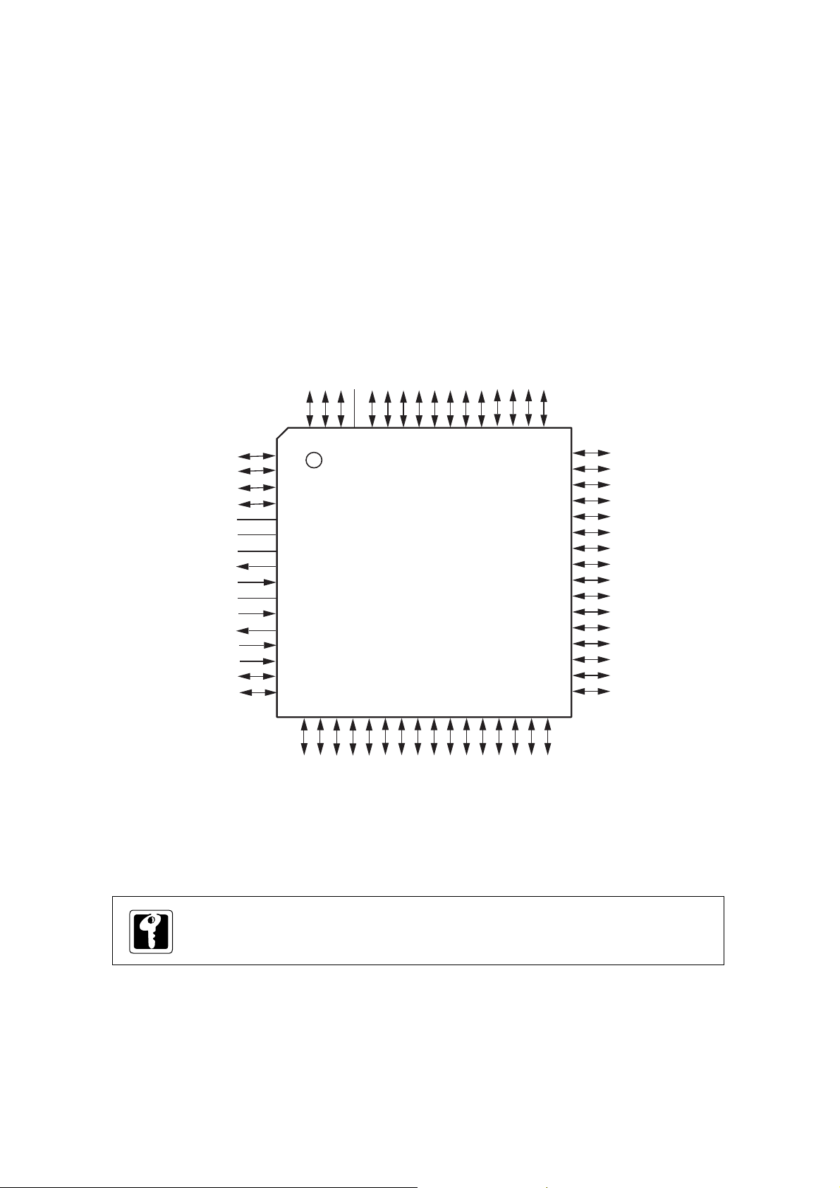
1-3-1 Pin Configuration
Chapter 1 Overview
AN3/PA3
AN4/PA4
AN5/PA5
AN6/PA6
NC(VPP)
VREF+
VDD
OSC2
OSC1
VSS
XI
XO
MMOD
NRST/P27
TXD1A/SBO1A/P00
SDA4B/RXD1A/SBI1A/P01
1
2
3
4
5
6
7
8
9
10
11
12
13
14
15
16
PA2/AN2
PA1/AN1/DA1
636261
64
171819
PA0/AN0/DA0
VREF-
P80/LED0
P81/LED1
P82/LED2
P83/LED3
P84/LED4
P85/LED5
P86/LED6
6059585756555453525150
MN101C77C
- 64 pin for general use -
20
2122232425262728293031
P87/LED7
P77/TCIO5
P76/TCIO1
P75/SBT1B
P74/SBI1B/RXD1B
49
48
47
46
45
44
43
42
41
40
39
38
37
36
35
34
33
32
P73/SBO1B/TXD1B
P72/SBT0B
P71/SBI0B/RXD0B
P70/SBO0B/TXD0B
P67/SDO7/KEY7
P66/SDO6/KEY6
P65/SDO5/KEY5
P64/SDO4/KEY4
P63/SDO3/KEY3
P62/SDO2/KEY2
P61/SDO1/KEY1
P60/SDO0/KEY0
P54/SCL4A
P53/SDA4A
P52/SBT3/SCL3
P51/SB03/SDA3
SBT0A/P05
BUZZER/P06
RXD0A/SBI0A/P04
SCL4B/SBT1A/P02
TXD0A/SBO0A/P03
RMOUTA/TCO0A/P10
IRQ0/P20
TCIO7/P14
TCO4A/P12
TCIO4B/P13
RMOUTB/TCIO0B/P11
IRQ2/P22
ACZ/IRQ1/P21
SBI3/P50
IRQ3/P23
IRQ4/P24
On Flash version of MN101CF77G, NC pin is VPP.
Figure 1-3-1 Pin Configuration ( 64 LQFP/64TQFP : Top view )
Pin Description
I - 9
Page 28

Chapter 1 Overview
1-3-2 Pin Specification
Table 1-3-2 Pin Specification
Pin
P00 SBO1A TXD1A in/out P0DIR0 P0PLU0 SBO1A : Serial Interface 1 transmission data output TXD1A : UART 1 transmission data output
P01 SBI1A RXD1A in/out P0DIR1 P0PLU1 SBI1A : Serial Interface 1 reception data input
P02 SBT1A in/out P0DIR2 P0PLU2 SBT1A : Serial 1 clock I/O
P03 SBO0A in/out P0DIR3 P0PLU3 SBO0A : Serial 0 transmission data output
P04 SBI0A in/out P0DIR4 P0PLU4 SBI0A : Serial 0 reception data input
P05 SBT0A in/out P0DIR5 P0PLU5 SBT0A : Serial 0 clock I/O
P06 BUZZER in/out P0DIR6 P0PLU6 BUZZER : Buzzer output
P10 TCO0A RMOUTA in/out P1DIR0
P11 TCIO0B in/out P1DIR1 P1PLU1 TCIOOB : Timer 0 I/O
P12 TCO4A in/out P1DIR2 P1PLU2 TCIO4A : Timer 4 I/O
P13 TCIO4B in/out P1DIR3 P1PLU3 TCIO4B : Timer 4 I/O
P14 TCIO7 in/out
P20 IRQ0 P2PLU0 IRQ0 : External interrupt 0
P21 IRQ1 P2PLU1 IRQ1 : External interrupt 1
P22 IRQ2 P2PLU2 IRQ2 : External interrupt 2
P23 IRQ3 P2PLU3 IRQ3 : External interrupt 3
P24 IRQ4 P2PLU4 IRQ4 : External interrupt 4
P27 NRST in/out - - NRST : Reset
P50
P51
P52 SBT3 in/out P5DIR2 P5PLU2 SBT3 : Serial interface 3 clock I/O
P53 in/out P5DIR3 P5PLU3
P54 in/out P5DIR4 P5PLU4
P60 SDO0 in/out P6DIR0 P6PLU0 KEY0 : KEY interrupt input 0
P61 SDO1 in/out P6DIR1 P6PLU1 KEY1 : KEY interrupt input 1
P62 in/out P6DIR2 P6PLU2
P63 SDO3
P64
P65
P66
P67
P70 in/out P7DIR0 P7PLUD0
P71 in/out P7DIR1 P7PLUD1
P72 in/out P7DIR2 P7PLUD2
P73 in/out P7DIR3 P7PLUD3
P74 in/out P7DIR4 P7PLUD4
P75 in/out P7DIR5 P7PLUD5
P76 in/out P7DIR6 P7PLUD6
P77 in/out P7DIR7 P7PLUD7
P80 LED0 in/out P8DIR0 P8PLU0 LED0 : LED driving pin 0
P81 LED1 in/out P8DIR1 P8PLU1 LED1 : LED driving pin 1
P82 LED2 in/out P8DIR2 P8PLU2 LED2 : LED driving pin 2
P83 LED3 in/out P8DIR3 P8PLU3 LED3 : LED driving pin 3
P84 LED4 in/out P8DIR4 P8PLU4 LED4 : LED driving pin 4
P85 LED5 in/out P8DIR5 P8PLU5 LED5 : LED driving pin 5
P86 LED6 in/out P8DIR6 P8PLU6 LED6 : LED driving pin 6
P87 LED7 in/out P8DIR7 P8PLU7 LED7 : LED driving pin 7
PA0 AN0 PAPLUD0 AN0 : Analog 0 input
PA1 AN1 PAPLUD1 AN1 : Analog 1 input
PA2 AN2 PAPLUD2 AN2 : Analog 2 input
PA3 AN3 PAPLUD3 AN3 : Analog 3 input
PA4 AN4 PAPLUD4 AN4 : Analog 4 input
PA5 AN5 PAPLUD5 AN5 : Analog 5 input
PA6 AN6 PAPLUD6 AN6 : Analog 6 input
Function
SDA4B
SBI3
SBO3
SDA4A
SCL4A
SDO2
SDO4
SDO5
SDO6
SDO7
SBO0B
SBI0B
SBT0B
SBO1B
SBI1B
SBT1B
TCIO1
TCIO5
SCL4B
TXD0A
RXD0A
RMOUTB
ACZ
SDA3
SCL3
KEY0
KEY1
KEY2
KEY3
KEY4
KEY5
KEY6
KEY7
TXD0B
RXD0B
TXD1B
RXD1B
DA0
DA1
Input/output
in/out
in/out
in/out
in/out
in/out
in/out P5DIR0 P5PLU0 SBO3 : Serial 3 reception data output
in/out P5DIR1 P5PLU1 SBI3 : Serial interface 3 ransmission data input
in/out P6DIR3 P6PLU3 KEY3 : KEY interrupt input 3
in/out
in/out P6DIR5 P6PLU5 KEY5 : KEY interrupt input 5
in/out
in/out
in/out
in/out
in/out
in/out
in/out
in/out
in/out
Direction
control
P1DIR4 P1PLU4 TCIO7 : Timer 7 I/O
P2DIR0
P2DIR1
P2DIR2
P2DIR3
P2DIR4
P6DIR4
P6DIR6
P6DIR7 P6PLU7 KEY7 : KEY interrupt input 7
PADIR0
PADIR1
PADIR2
PADIR3
PADIR4
PADIR5
PADIR6
Pin control
SDA4B :
Serial Interface 4
P1PLU0 TCIO0A : Timer 0 output
SDA4A : Serial interface 4 data I/O
SCL4A : Serial interface 4 clock I/O
SDO0 : Timer synchronous output 0
SDO1 : Timer synchronous output 1
SDO2 : Timer synchronous output 2
SDO3 : Timer synchronous output 3
SDO4 : Timer synchronous output 4
P6PLU4
SDO5 : Timer synchronous output 5
SDO6 : Timer synchronous output 6
P6PLU6
SDO7 : Timer synchronous output 7
SBO0B : Serial interface 0 transmission data output
SBI0B : Serial interface 0 reception data input
SBT0B : Serial interface 0 clock I/O
SBO1B : Serial interface 1 transmission data output
SBI1B : Serial interface 1 reception data input
SBT1B : Serial interface 1 clock I/O
TCIO1 : Timer 1 I/O
TCIO5 : Timer 5 I/O
Descreption
data I/O
RXD1A : UART 1 reception data output
SCL4B :
Serial Interface 4 clock I/O
TXD0A : UART 0 transmission data output
RXD0A : UART 0 reception data input
RMOUTA : Remote control carrier output
RMOUTB : Remote control carrier output
ACZ : AC zero bolt detection input
SDA3 :
Serial Interface 3 data I/O
SCL3 :
Serial Interface 3 clock I/O
KEY2 : KEY interrupt input 2
KEY4 : KEY interrupt input 4
KEY6 : KEY interrupt input 6
TXD0B : UART 0 transmission data output
RXD0B : UART 0 reception data output
TXD1B : UART 1 transmission data output
RXD1B : UART 1 reception data output
DA0 : DA0 output
DA1 : DA1 output
I - 10
Pin Description
Page 29

1-3-3 Pin Functions
Table 1-3-3 Pin Function Summary (1/6)
Name No. I/O Funct ion Ot her Funct ion Description
VDD 7 Power supply pin
VSS 10
OSC1 9 Input Clock input pin
OS C 2 8 Output Clock output pin
Supply 1.8 V to 3.6 V to VDD and 0 V to VSS.
Connect these oscillation pins to cer amic or
crystal oscillat ors for high-frequency c loc k
operation.
If the clock is an external input, connect it to OSC1
and leave OSC2 open. T he chip will not oper at e
with an external c lock when using either the
STOP or SLOW modes.
Chapter 1 Overview
XI 11 Input Clock input pin
XO 12 Out put Clock output pin
NRST 14 I/O Reset pin P27 This pin resets the chip when power is turned on,
P00 15 I/O I/O port 0 SBO1A, TXD1A
P01 16 SBI1A, RXD1 A
SDA4B
P02 17 SBT1A , SCL4B
P03 18 SBO0A , T XD0A
P04 19 SBI0A, RXD0 A
P05 20 SBT0A
P06 21 BUZZER
P10 22 I/O I/O port 1 TCO0A, RMOUTA
P11 23 TCIO0B, RMOUTB
P12 24 TCO4A
P13 25 TCIO4B
P14 26 TCI07
Connect these oscillation pins to cer amic
oscillators or crystal oscillators for low-fr equency
clock operation.
If the clock is an external input, connect it to XI
and leave XO open. The c h ip will not operate with
an ex ternal clock when using the STOP mode. If
these pins are not used, connect XI to VSS and
leav e XO open.
is allocated as P27 and contains an internal pullup resistor. S etting this pin low initializes the
internal state of the device. Thereafter, setting the
input to high r eleases the reset. The hardware
waits for t he sy stem clock to stabilize, then
processes the reset int errupt. Also, if ""0" " is
written to P27 and the reset is initiated by
softwar e, a low level will be out put. The output
has an n-channel open-drain configur ation. I f a
capacitor is to be inserted between NRST and
VDD, it is recommended that a discharge diode
be placed between NRST and VDD.
7-Bit CMOS tri-state I/O port.
Eac h bi t can b e set in di vi dual l y as either an in put
or output by the P0DIR register. A pull-up resistor
for eac h bit c an be selected individually by the
P0PLU register.
At reset, the input mode is selected and pull-up
resistors are disabled (high impedance output) .
5-Bit CMOS tri-state I/O port.
Eac h bi t can b e set in di vi dual l y as either an in put
or output by the P1DIR register. A pull-up resistor
for eac h bit c an be selected individually by the
P1PLU register.
At reset, the input mode is selected and pull-up
resistors are disabled (high impedance output) .
Pin Description
I - 11
Page 30

Chapter 1 Overview
Table 1-3-4 Pin Function Summary (2/6)
Name No. I/O F unctio n Other Function Description
P20 27 I/O I/O port 2 IRQ0
P21 28 IRQ1, ACZ
P22 29 IRQ2
P23 30 IRQ3
P24 31 IRQ4
P27 14 Input I /O port 2 NRST P27 has an n-channel open-drain configurati on.
P50 32 I/O I/O port 5 SBI3
P51 33 SBO3,
P52 34 SBT3
P53 35 SDA4A
P54 36 SCL4A
P60 37 I/O I/O port 6 SDO0, KEY0
P61 38 SDO1, KEY 1
P62 39 SDO2, KEY 2
P63 40 SDO3, KEY 3
P64 41 SDO4, KEY 4
P65 42 SDO5, KEY 5
P66 43 SDO6, KEY 6
P67 44 SDO7, KEY 7
P70 45 I/O I/O port 7 SBO0B, TXD0B
P71 46 SB I0B, RXD0B
P72 47 SBT0B
P73 48 SBO1B, TX D1B
P74 49 SB I1B, RXD1B
P75 50 SBT1B
P76 51 TCI01
P77 52 TCI05
P80 60 I/O I/O port 8 LED0
P81 59 LED1
P82 58 LED2
P83 57 LED3
P84 56 LED4
P85 55 LED5
P86 54 LED6
P87 53 LED7
PA0 62 I/O I/O port A AN0, DA0
PA1 63 AN1, DA1
PA2 64 AN2
PA3 1 AN3
PA4 2 AN4
PA5 3 AN5
PA6 4 AN6
5-Bit CMOS tri-state I/O port.
A pull-up resistor for each bi t can be select e d
individually by the P2PLU register .
At reset, pull-up r esistor s are d isabled
(high impedance output ) .
When "0" is written and the reset is initiated by
softwar e, a low level will be out put.
5-Bit CMOS tri-state I/O port.
Each bit can be set individually as either an input
or output by the P5 DIR register . A pul l-up resistor
for eac h bit c an be selected individually by the
P5PLU register. At reset, the P50t o P54 input
mode is selected and pull- up resistors are
disabled. (high impedance output)
8-Bit CMOS tri-state I/O port.
Each bit can be set individually as either an input
or output by the P6 DIR register . A pul l-up resistor
for eac h bit c an be selected individually by the
P6PLU register.
At reset, the P60 to P67 input mode is selected
and pull- up resistors are disabled.
(high impedance output )
8-Bit CMOS tri-state I/O port.
Each bit can be set individually as either an input
or output by the P7 DIR register . A pul l-up/pulldown resistor for each bit can be selected
individually by the P7PLU r e gist e r . Howev er,
pull-up and pull-down resistors cannot be mixed.
At reset, the P70to P77 input mode is selected
and pull- up resistors are disabled. (high
impedance output )
8-Bit CMOS tri-state I/O port. Each bit can be set
individu al ly as either an input or output by the
P8DIR register. A pull-up resistor for each bit c an
be selected individually by the P8PLU register.
When c o nfigured as out puts, these pins can
drive LEDs directly. A t reset, the P80to P 87 input
mode is selected and pull- up resistors are
disabled. (high impedance output)
6-Bit I/O port. A pull-up or pull-down resistor for
each bi t can be selected individually by the
PAPLUD resister. However, pull-up and pulldown resistors cannot be mixed. At reset, the
PA0 to PA 6 input mode is selected and pull- up
resistor s are di sabled. (high impedance ou tput)
I - 12
Pin Description
Page 31

Table 1-3-5 Pin Function Summary (3/6)
Name No. I/O Function Other Function Description
SBO 0A 18 Output P03, TXD0A
SBO0B 48 P70, TXD0B
SBO1A 15 P00, TXD1A
SBO1B 45 P73, TXD1B
SBO3 33 P51, SDA3
SBI 0A 19 Input P04, RXD0A
SBI0B 49 P71, RXD0B
SBI1A 16 P01, RXD1A
SBI1B 46 P74, RXD1B
SBI3 32 P50
Serial interface
transmission data
output pins
Serial interface
recept ion dat a input
pins
SDA4A
Transmission data output pins for serial
interfaces 0 , 1, 3. The output configuration,
eit her CMOS push-pull or n-channel op en-drain
can be selected. Pull-up r esistors can be
selected by the P0PLU register, the P5PLU
register and the P7PLUD r egister. S elec t output
mode by the P0DI R register , the P5DI R register
and the P7DI R r egister, and serial data output
mode by serial mode register 1 ( S C0MD1,
SC1M D1, SC3MD1). These can be used as
normal I/O pins when the serial interfac e is not
used .
Reception data input pins for serial inter faces 0,
1, 3. Pll-up resistors can be selected by the
P0PLU register, the P5PLU register and the
P7PLUD register. Select input mode by the
P0DIR register, the P5DI R r egister, the P7DIR
register and serial input mode by the serial mode
regist er 1 ( S C0MD1, S C1 MD1, S C 3MD1). These
can be u sed as normal I /O pins when t he seri al
interface is not used.
Chapter 1 Overview
SBT0A 20 I/O P50
SBT0B 50 P72
SBT1A 17 P02, SCL4A
SBT1B 47 P75
SBT3 34 P52, SCL3
TXD0A 18 Output SBO0A, P03
TXD0B 48 SBO0B, P70
TXD1A 15 SBO1A, P00
TXD1B 45 SBO1B, P73
Serial interface
clock I/O pins
UART tr an smission
data output pins
Clock I /O pins for serial interf ac es 0, 1, 3. The
output configuration, either CMOS push-pull or nchannel op en - drain can be selected. Pull - up
resist o rs ca n be selected by the P0P LU re sister
and the P5PLU register and t he P 7PLUD
register. Select clock I/O for each communication
mode by the P0DI R register , the P5DI R register ,
the P7DIR register and serial mode register 1
( SC0MD1, SC1M D1, S C3MD1). T hese can be
used as normal I/O pins when the serial interf ace
is not used.
In the serial interface in UART mode, these pins
are configured as the transmission data output
pins. The output configurati on, either CMOS
push-pull or n-channel open -drain can be
selected. Pull-up resistors can be selected by
the P0PLU r egister and t he P 7PLUD register.
Select out put mode by the P0DIR register and the
P7DIR register, and serial data output by serial
interface 1 mode register 1 ( SC0MD1, SC1MD1).
These can be used as normal I/O pins when the
serial interfac e i s not used.
Pin Description
I - 13
Page 32

Chapter 1 Overview
Table 1-3-6 Pin Function Summary (4/6)
Name No. I/O Function Other Function Description
RX D0A 19 Input S B I 0A, P04
RXD0B 49 SBI0B, P71
RXD1A 16 SBI1A, P01
RXD1B 46 SBI1B, P74
UART reception
data input pin
SDA4A
In t he serial interfac e in UART mode, these pins
are configured as the received data input pin.
Pull-up resistors can be selected by the P0PLU
register and P7PLUD register. Set this pin to the
input mode by t he P0DI R r egister and the P 7DI R
register, and to the serial input mode by the serial
interf ace1 mode register 1 ( SC0MD1, SC1MD1).
This can be used as normal I/O pin when t he
serial interface is not used.
TCO0A 22 I/O P10, RMOUT
TCI00B 23 P11
TCI01 51 P12
TCO4A 24 P13
TCI04B 25 P37
TCI05 52 P77
SDA4A 16 I/O P01, SBI1A
SDA4B 35 P53
SCL4A 17 I/O P02, SBT1A,
SCL4B 36 P54
RMOUT 22 I/O Remote control
Timer I/O pins
Serial interface
data I/O pins
Serial interf ac e 4
clock I/O pins
transmission
signal output pin
RXD1A
P10,T CO0A Out put pin for remote cont r ol t r ansmission signal
Event counter clock input pins, overflow pulse
and PWM signal output pins for 8-bit timers 0 , 1,
4, 5. To use these pins as ev ent clock inputs,
configure t hem as inputs by t he P 1DI R and
P7DIR register. When the pins are used as
inputs, pull-up resistors can be specified by the
P1PLU, P 7P LUD register. F or overflow pulse,
PWM signal output, select the special function pin
by the port 1 out put mode register (P1OMD) and
set to the out put mode by the P1DIR register.
When not used for timer I/O, these can be used
as normal I/O pins.
Reception data input pins for serial interfac es 4.
During data communications, select n-channel
open-drain to comply wit h IIC communication
standard. Pull-up resistors can be selected by
the P0PLU r egister and the P 5PLU r egister.
During data communications, select output mode
by the P0DIR register and the P5DIR register.
These can be used as normal I/O pins when the
serial interface is not used.
Clock I/O pins for serial interfaces 4. During data
communications, select n- channel open-drain to
comply with IIC communication standard. Pull-up
resistors can be selected by the P0PLU resister
and the P5PLU register. During dat a
communications, select out put mode by the
P0DIR register and the P5DIR register. These
can be used as normal I/O pins when the serial
interf ac e is not used.
with a carrier signal. For remote cont r ol c arrier
output, select the special function pin by the port
1 output mode register (P1O MD) and set to the
output mode by the P1DIR register. Also, set to
the remote control carrier output by the remote
control c arr ier output cont rol r egister (RMCTR).
This can be used as a normal I/O pin when
remote control is not used.
I - 14
Pin Description
Page 33

Chapter 1 Overview
Table 1-3-7 Pin Function Summary (5/6)
Name No. I/O Function Other Function Description
BUZZER 21 Output Buzzer out put P06 Piezoelectric buzzer dr iver pin. The driving
frequency can be selected by the DLYCT R
register. Select output mode by the P0DIR
register and select P 06 buzzer out put by the
DLY CTR register. W hen not used for buzzer
output, this pin can be used as a normal I/O pin.
TCI 07 26 I/O Timer I/ O pin P14 Event counter cloc k input pin, overflow pulse and
PWM signal output pin for 16-bit timer 7. T o use
this pin as event cloc k input , configure this as
input by the P1DIR register. In the input mode,
pull-up resistors can be selected by the P1PLU
register. F or overflow pulse, PWM signal output,
select the special function pin by the port 1 output
mode register (P1O MD), and set to t he output
mode by the P1DIR register. W hen not used for
timer I/O, this can be used as normal I/O pin.
VREF+ 6
VREF- 61 - - power supply for
AN0 62 Input A nalog input pins PA 0, DA0
AN1 63 PA1, DA1
AN2 64 PA2
AN3 1 PA3
AN4 2 PA4
AN5 3 PA5
AN6 4
DA 0 62 Output Analog output pins PA0, AN0
DA 1 63 PA1, A N 1
IRQ0 27 Input P20
IRQ1 28 P21, ACZ
IRQ2 29 P22
IRQ3 30 P23
IRQ4 31 P24
A CZ 28 Input AC zero-cross
+ power supply for
A/D converter
A/D converter
External interrupt
input pins
detect ion input pin
PA6
P21, IRQ1 An input pin for an AC zero-cross detection circuit.
Reference power supply pins for the A /D
converter. Normally, the values of VDD=VREF+
and VSS=VREF - ar e used. W h en t he y are not
used, the v alues should be VRE F+=VDD and
VREF-=VSS.
Analog input pins for an 7-channel, 10-bit A/D
conv er ter. When not used for analog input, these
pins can be used as normal I/O pins.
Analog output pins for an 2-channel, 8-bit D/A
conv er ter. When not used for analog output,
these pins can be u sed as normal I/O pins.
External interrupt input pins. T he valid edge for
IRQ0 to 4 can be selected with the IRQnICR
register. IRQ1 is an external interrupt pin that is
able to deternine AC zero c rossings. Both edge
for IRQ0 to 4 are valid for interrupt. When these
are not used for inter rupt s, t hese can be used as
normal input pins.
The AC zero-c r oss detection circuit outputs a high
level when the input is at an intermediate level. It
outputs a low level at all ot her t imes. A CZ input
signal is connected to the P 21 input c irc uit and
the IQR1 interrupt circuit. When the AC zero-cross
detect ion circ uit is not used, this pin can be used
as a normal P21 input.
Pin Description
I - 15
Page 34

Chapter 1 Overview
Table 1-3-8 Pin Function Summary (6/6)
Name No. I/O Function Other Function Description
KEY 0 37 I/ O P60, SDO0
KEY 1 38 P61, SDO1
KEY 2 39 P62, SDO2
KEY 3 40 P63, SDO3
KEY 4 41 P64, SDO4
KEY 5 42 P65, SDO5
KEY 6 43 P66, SDO6
KEY 7 44 P67, SDO7
M MOD 17 Input Memory mode
Key inter r upt input
pins
switching input
pins
Input pins for interrupt based on ORed result of
pin inputs. K ey input pin for 2 bits can be
selected individually by the key interrupt control
register (P6M D). W hen not used for KEY input,
these pins can be used as normal I/O pins.
This pin sets the memory expansion mode.
AIways set the input low.
I - 16
Pin Description
Page 35

1-4 Block Diagram
1-4-1 Block Diagram
XO
XI
OSC1
OSC2
VSS
VDD
Chapter 1 Overview
MMOD
TXD1A,SBO1A,P00
SDA4B,RXD1A,SBI1A,P01
SCL4B,SBT1A,P02
TXD0A,SBO0A,P03
RXD0A,SBI0A,P04
SBT0A,P05
BUZZER,P06
RMOUTA,TCO0A,P10
ROMUTB,TCIO0B,P11
TCO4A,P12
TCIO4B,P13
TCIO7,P14
IRQ0,P20
ACZ,IRQ1,P21
IRQ2,P22
IRQ3,P23
IRQ4,P24
NRST,P27
Port 0
Port 1 Port 2
Low Speed
oscillator
8-Bit Timer 0
8-Bit Timer 1
8-Bit Timer 4
8-Bit Timer 5
16-Bit Timer 7
High Speed
oscillator
ROM
48KB
A/D converter
D/A converter
CPU
MN101C
RAM
3KB
External Interrupt
Serial Interface 0
Serial Interface 1
Serial Interface 3
Serial Interface 4
Time Base Timer 6
Watchdog Timer
Automatic Transfer Controller
Port 5 Port 6
Port A Port 8
Port 7
PA6,AN6
PA5,AN5
PA4,AN4
PA3,AN3
PA2,AN2
PA1,AN1,DA1
PA0,AN0,DA0
P87,LED7
P86,LED6
P85,LED5
P84,LED4
P83,LED3
P82,LED2
P81,LED1
P80,LED0
P77,TCIO5
P76,TCIO1
P75,SBT1B
P74,SBI1B,RXD1B
P73,SBO1B,TXD1B
P72,SBT0B
P71,SBI0B/RXD0B
P70,SBO0B,TXD0B
VREF-
VREF+
SBI3,P50
SDA4A,P53
SCL3,SBT3,P52
SDA3,SBO3,P51
SCL4A,P54
Figure 1-4-1 Block Diagram
KEY2,SDO2,P62
KEY1,SDO1,P61
KEY0,SDO0,P60
KEY5,SDO5,P65
KEY4,SDO4,P64
KEY3,SDO3,P63
KEY7,SDO7,P67
KEY6,SDO6,P66
Block Diagram
I - 17
Page 36

Chapter 1 Overview
1-5 Electrical Characteristics
This LSI user's manual describes the standard specification.
System clock ( fs ) is 1/2 of high speed oscillation at NORMAL mode, or 1/4 of low speed oscillation at SLOW mode.
Please ask our sales offices for its own product specifications.
Contents
Model
Structure
Application
Function
MN101C77
CMOS integrated circuit
General purpose
8-Bit single-chip microcontroller
1-5-1 Absolute Maximum Ratings
Parameter
1
2 Input clamp volt age
Input pin voltage
3
Output pin volta ge
4
I/O pin voltage
5
6
Peak ou tput
7
current
Port 8 *4
Other than Port 8
8
9
Aver ag e ou tput
10
current *1
Port 8 *4
Other than Port 8
11
Symbo l
V
DD
Ic -500 to +500
V
I
V
O
V
IO
I
(peak)
OL1
(peak)
I
OL2
I
(peak)
OH
(avg)
I
OL1
I
(avg)
OL2
(avg) -5
I
OH
*2,*3
(voltages referenced to Vss)
- 0.3 to +4.6
-0.3 to V
-0.3 to V
-0.3 to V
DD
DD
DD
+0.3
+0.3
+0.3
30
10
-10
20
5
UnitRating
µ
mA
VPower supply voltage
A
V
I - 18
Power dissipation 300
12
Operating ambient t emperature
13
Stor age t emperatur e
14
P
D
T
opr
T
stg
-40 to +85
-40 to +125 *5
*1 Applied to any 100 ms period.
*2 Connect at least one bypass capacitor of 0.1 µF or larger between the power
supply pin and the ground for latch-up prevention.
*3 The absolute maximum ratings are the limit values beyond which the LSI may
be damaged and proper operation is not assured.
*4 Applied when P8LED register outputs LED.
*5 -40 to + 98 (°C) for the Flash EEPROM version.
Electrical Characteristics
mW
o
C
Page 37

Chapter 1 Overview
V
1-5-2 Operating Conditions
[ NORMAL mode : fs=fosc/2, SLOW mode : fs=fx/2 ]
Parameter Symbol Conditions Unit
Power supply voltage
< 20. 00 MHz
f
1
2
Power supply voltage
3
4
Voltage to maintain RAM data V
5
V
V
V
V
osc
DD1
f
= f
s
osc
< 10. 00 MHz
f
osc
DD2
= f
f
s
osc
< 4.00 MHz
f
osc
DD3
= f
f
s
osc
fx = 32.768 kHz
DD4
= f
f
s
osc
During STOP mode
DD5
/2
/2
/2
/2
Operat ion speed *1
t
6
7t
8t
Min imum instruction
ex ec ut ion t ime
V
c1
c2
c3
= 2.5 V to 3.6 V
DD
= 2.1 V to 3.6 V
V
DD
= 1.8 V to 3.6 V
V
DD
Ta=-40 oC to +85 oC
MIN TYP MAX
2.5
2.1
1.8
1.8
1.8
0.1
0.2
0.5
V
=1.8 V to 3.6 V, VSS=0
DD
Rating
3.6
3.6
3.6
3.6
3.6
V
s
µ
V
9t
c4
= 1.8 V to 3.6 V
DD
Crystal osillator 1 Figure 1-5-1
Crystal frequency f
10
11
External capasitors
12
Int er nal f eedback resistor R
13
xtal 1
C
11
C
12
F10VDD
V
= 2.5 V to 3.6 V 1. 0 20.0 MHz
DD
= 3. 3 V 1000 k
Crystal osillator 2 Figure 1-5-2
Crystal frequency f
14
15
External capasitors
16
Int er nal f eedback resistor R
17
VDD=1.8 V to 3.6 V 32.768 kHz
xtal 2
C
21
C
22
F20VDD
=3.3 V
*1 tc1, tc2, tc3 : 1/2 of high speed oscillation
tc4 : 1/2 of high speed oscillation
OSC1
F10
R
MN101C
OSC2
f
xtal1
C
12
C
11
RF20
MN101C
61.04
47
pF
47
Ω
22
pF
22
6.0 M
XI
xtal2
f
XO
C
22
C
21
Ω
The feedback resistor is built-in.
The feedback resistor is built-in.
Figure 1-5-1 Crystal Oscillator 1 Figure 1-5-2 Crystal Oscillator 2
Electrical Characteristics
I - 19
Page 38

Chapter 1 Overview
Ta=-40 oC to +85 oC
=1.8 V to 3.6 V VSS=0 V
V
DD
Parameter Symbol Conditions Unit
Externa l c l oc k in put 1 OSC1 (OS C 2 is opened)
Clock frequency f
18
High level pulse width
19
osc
t
wh1
20.0
*1 Figure 1-5-3
Low level pulse width
20
Rising time
21
t
wl1
t
wr1
20.0
Figure 1-5-3
Falling time
22
t
wf1
Externa l c l oc k in put 2 XI (XO is opened)
Clock frequency
23
High level pulse width
24
f
x
t
wh2
*1 Figure 1-5-4
Low level pulse width
25 3.5
Rising time
26
t
wl2
t
wr2
Figure 1-5-4
Falling time t
27
wf2
Rating
MIN TYP MAX
1.0 20.0
5.0
5.0
32.768
3.5
20
20
MHz
ns
kHz
µ
ns
s
*1 The clock duty rate should be 45% to 55%.
Certain operating conditions differ between the mask ROM version and the Flash version.
Refer to chapter 18 Flash EEPROM for electrical characteristics of the Flash version.
I - 20
Electrical Characteristics
Page 39

twh1 twl1
Chapter 1 Overview
0.9VDD
0.1VDD
twr1
twc1
Figure 1-5-3 OSC1 Timing Chart
twh2 twl2
twf1
0.9VDD
0.1VDD
twr2
twf2
twc2
Figure 1-5-4 XI Timing Chart
Electrical Characteristics
I - 21
Page 40

Chapter 1 Overview
V
1-5-3 DC Characteristics
Ta=-40 oC to +85 oC
=1.8 V to 3.6 V VSS=0
V
DD
Parameter Symbol Conditions Unit
Power supply curr ent (not load at output pin) *1
f
=20. 00 MHz,VDD=3.3 V
1
2
I
I
Power supply current
3
4
I
I
5I
Supply curren t dur ing
HALT1 mode
6I
7I
Supply curren t dur ing
STOP mode
8I
osc
DD1
[fs = f
/2]
osc
=8.39 MHz,VDD=3.3 V
f
osc
DD2
[f
= f
/2]
s
osc
fx=32.768 kHz ,VDD=3.3 V
DD3
DD4
DD5
DD6
DD7
DD8
= fx/2] Ta=25 oC
[f
s
f
=32.768 kHz ,VDD=3.3 V
x
= fx/2] Ta=-40 oC to +85 oC
[f
s
f
=32.768 kHz ,VDD=3.3 V
x
o
Ta=25
fx=32.768 kHz ,VDD=3.3 V
Ta=-40 oC to +85 oC
VDD=3.3 V
o
Ta=25
VDD=3.3 V
Ta=-40
C
C
o
C to +85 oC
Rating
MIN TYP MAX
126
36
10 20
40
510
40
02
30
mA
A
µ
*1 Measured under conditions of Ta=25 °C, without load.
- The supply current during operation, IDD1(IDD2), is measured under the following conditions:
After all I/O pins are set to input mode and the oscillation is set to <NORMAL mode>, the
MMOD pin is connected to VSS level, the input pins are connected to VDD level, and a 20 MHz
(8.39 MHz) square wave of VDD and VSS amplitude is input to the OSC1 pin.
- The supply current during operation, IDD3(IDD4), is measured under the following conditions:
After all I/O pins are set to input mode and the oscillation is set to <SLOW mode>, the MMOD pin
is connected to VSS level, the input pins are connected to VDD level, and a 32.768 kHz square wave
of VDD and VSS amplitude is input to the XI pin.
- The supply current during HALT mode, IDD5(IDD6), is measured under the following conditions:
After all I/O pins are set to input mode and the oscillation is set to <HALT mode>, the MMOD pin
is connected to VSS level, the input pins are connected to VDD level and an 32.768 kHz square wave
of VDD and VSS amplitude is input to the XI pin.
- The supply current during STOP mode, IDD7(IDD8), is measured under the following conditions:
After the oscillation is set to <STOP mode>, the MMOD pin is connected to VSS level, the input pins
are connected to VDD level, and the OSC1 and XI pins are unconnected.
I - 22
Electrical Characteristics
Page 41

Chapter 1 Overview
Parameter Symbol Conditions Unit
Input pin 1 MMOD
Input high voltage
9
Input low voltage
10
Input leak age cur r ent
11
Input pin 2 P21 (at used as ACZ)
Input high voltage 1 V
12
Input low voltage 1
13
Input high voltage 2
14
Input low voltage 2
15
Input leak age cur r ent
16
Rising time t
17
V
V
18
V
V
V
IH1
IL1
I
LK1
DHH
DLH
DHL
DLL
I
LK2
IN
V
DD
Figure 1-5-5
VIN=0 V to V
rs
Figure 1-5-5
fs
=0 V to V
=3.3 V
DD
DD
Ta = -40 oC to +85 oC
MIN TYP MAX
0.8V
DD
0
2.9 V
V
SS
1.1
V
SS
30
30Falling t ime t
VDD=1.8 V to 3.6 V VSS=0 V
Rating
V
DD
0.2V
DD
10
±
DD
2.1
V
DD
0.4
10
±
V
AV
µ
V
A
µ
s
µ
Input voltage level 1
Input voltage level 2
( Input )
( Output )
trs
t
fs
Figure 1-5-5 AC Zero-Cross Detector
DD
V
V
DHH
V
DLH
V
DHL
V
DLL
V
SS
Electrical Characteristics
I - 23
Page 42

Chapter 1 Overview
Ta=-40 oC t o +85 oC
=1.8 V to 3.6 V VSS=0 V
V
DD
Param eter Sym bol Conditions Unit
I nput pin 3 P27 (NRST)
I nput high volt age
19
Input low voltage V
20
I nput high current I
21
V
IH3
IL3
VDD=3.3 V,V
IH3
Pull-up resistor is built-in
IN=VSS
I/O pin 4 PA0 to PA6
I nput high volt age
22
Input low voltage V
23
I nput leakage current VIN=0 V to V
24
I nput high current I
25
Input low current I
26
Output high voltage
27
Output l ow voltage
28
V
IH4
IL4
LK4
V
=3.3 V,VIN=V
IH4
V
OH4
V
DD
Pull -up resistor is ON
VDD=3.3 V,VIN=V
IL4
Pull-down resistor is ON
V
=3.3 V, IOH=-2.0 mA
DD
=3.3 V, IOL=2.0 mA
V
DD
OL4
DD
SS
DD
I/O pin 5 P00 to P06, P10 to P14, P20 to P24, P50 to P54, P60 to P67
Rating
MIN TYP MAX
0.8V
DD
0
0.2V
-30 -100 -300
0.8V
DD
0
-30
30
0.2V
-100
100
2.7
(Schmitt trigger input)
V
DD
V
DD
2I
±
-300
300
0.4
DD
DD
V
A
µ
V
A
µ
V
I nput high volt age V
29
IH5
0.8V
DD
V
DD
V
Input low voltage
30
I nput leakage current
31
I nput high current
32
Output high voltage V
33
V
IL5
VIN=0 V to V
I
LK5
VDD=3.3 V,VIN=V
I
IH5
Pull -up resistor is ON
V
=3.3 V, IOH=-2.0 mA
OH5
DD
DD
0
SS
-30
2.7
0.2V
10
±
-100 -300
DD
A
µ
V
Output l ow voltage V
34
OL5VDD
=3.3 V, IOL=2.0 mA
0.4
I/O pin 6 P70 to P77 (Schmitt trigger input)
I nput high volt age V
35
IH6
0.8V
DD
V
DD
V
Input low voltage
36
I nput leakage current I
37
I nput high current I
38
Input low current I
39
Output high voltage V
40
V
IL6
=0 V to V
V
LK6
IH6
OH6VDD
IN
=3.3 V,VIN=V
V
DD
Pull -up resistor is ON
VDD=3.3 V,VIN=V
IL6
Pull-down resistor is ON
=3.3 V, IOH=-2.0 mA 2.7
DD
SS
DD
0
-30
30
0.2V
10
±
-100 -300
100 300
DD
A
µ
V
41
OL6VDD
=3.3 V, IOL=2.0 mA
0.4Output l ow voltage V
I - 24
Electrical Characteristics
Page 43

Chapter 1 Overview
I/O pin 7 P80 to P87
Inpu t high v oltage V
42
Inpu t low voltage V
43
Inpu t leakage curr e nt I
44
Inpu t high curren t I
45
Output high voltage V
46
Output low v o lt a ge V
47
Output low voltage (LE D)
48
IH7
IL7
LK7
IH7
OH7VDD
OL7VDD
V
OLL7VDD
Ta=-40
VIN=0 V to V
VDD=3.3 V,VIN=V
o
C to +85 oC
DD
SS
Pull-up r esistor is ON
=3.3 V, IOH=-2.0 mA
=3.3 V, IOL=2.0 mA
=3.3 V, I
=15.0 mA 1.0
OLL
VDD=1.8 V to 3.6 V VSS=0 V
Rating
MIN TYP MAX
0.8V
0
DD
V
0.2V
10
±
DD
DD
-30V-100 -300
2.7
0.4
UnitParam eter Sym bol Conditions
V
A
µ
Electrical Characteristics
I - 25
Page 44

Chapter 1 Overview
1-5-4 A/D Converter Characteristics *2
Ta=-40 oC to +85 oC
= 3.3 V VSS=0 V
V
DD
Param eter Symbol Conditions
Resolution
1
Non-linearity error 1
2
Dif ferential non-linearity
3
error 1
Non-linerarit y error
4
Dif ferential non-linearity
5
error 2
Zero transition voltage
6
Ful l-scale transition
7
voltage
8
A/D conversion time
9
10
S ampl ing time
11
12
Reference voltage
13
V
V
REF+
REF-
V
= 3.3 V,VSS = 0 V
DD
V
= 3.3 V,V
REF+
T
= 800 ns
AD
V
= 3.3 V,VSS = 0 V
DD
V
= 3.3 V,V
REF+
T
= 15.26 µs
AD
V
= 3.3 V,VSS = 0 V
DD
V
= 3.3 V,V
REF+
T
= 800 ns
AD
= 800 ns
T
AD
T
= 15.26 µs
AD
T
= 1.0 µs
AD
TAD = 15.26 µs
*1
*1
REF-
REF-
REF-
= 0 V
= 0 V
= 0 V
Rating
MIN TYP MAX
25 80
3220
3275
9.6
183
2
30.5
V
REF-
V
SS
V
0.5
10
±
±
±
±
18
DD
Unit
Bits
3
3
LSB
5
5
mV
s
µ
V
Analog inp ut voltage V
14
Analog inp ut leakage
15
current
Reference voltage pin
16
input leakage curr ent
Ladder resistance R
17
unselected channel
V
= 0 V to V
ADIN
Lader resistor OFF
V
REF-
<
laddVDD
= 3.3 V 20
V
REF+
DD
V
DD
<
REF-
*1 Set the potential difference between VREF+ and VREF- over 2 V.
*2 The value is measured with A/D Converter, not with D/A Converter.
V
REF+
2
±
10
±
50 80 k
A
µ
Ω
I - 26
Electrical Characteristics
Page 45

1-5-5 D/A Converter Characteristics *2
Ta = -40 oC to +85 oC
V
= 3.3 V V
DD
Chapter 1 Overview
= 0 V
SS
Parameter Symbol
Resolution *1
1
Reference voltage low lev el
2
Reference voltage high level
3
Zero-scale output voltage *1 V
4
Full- scale output voltage *1 V
5
A n alog output resistance
(minimum reference resistance)*1R
6
Non-linearity e r r o r N
7
Diff erenc t ial non-linearit y error
8
*1
9 Settling time *1 T
V
V
D
Conditions
REF-
REF+
V
= 3.3 V, V
REF+
ZS
D7 to D0=ALL"L"
V
= 3.3 V, V
REF+
FS
D7 to D0=ALL"H"
OUT
V
LE
NLE
SET
= 3.3 V, V
REF+
= 3.3 V, V
V
REF+
External capacitor CL = 35 pF
All bits are set to ON or OFF
REF-
REF-
REF-
REF-
= 0 V
= 0 V
= 0 V
= 0 V
Rating
MIN TYP MAX
8
0
2.0
3.20
7.0
0.0
3.29
11.0 15.0 k
0.5
±
0.5
±
0.5
V
DD
0.05
1.0
±
1.5
±
2.0
Unit
Bits
V
Ω
LSB
s
µ
*1 The standard value is guaranteed under condition of VDD=VREF+=3.3 V, VREF-=0.0 V .
*2 The value is measured with D/A Converter, not with A/D Converter.
Precautions
I - 27
Page 46

Chapter 1 Overview
1-6 Precautions
1-6-1 General Usage
Connection of VDD pin, and VSS pin
All VDD pins should be connected directly to the power supply and all Vss pins should be connected to
ground in the external. The following shows the correct connections and the incorrect connections. Please
consider the LSI chip orientation before mounting it on the printed circuit board. Incorrect connection may
lead a fusion and break a micro controller.
Cautions for Operation
(1) If you install the product close to high-field emissions (under the cathode ray tube, etc), shield
the package surface to ensure normal performance.
(2) Please consider the operation temperature. The guaranteed operation temperature differs on each
model. For example, if temperature is over the operating condition, its operation may be executed
wrongly.
(3) Please consider the operation voltage. The guaranteed operation voltage differs on each model.
-If the operation voltage is over the operation range, it can be shortened the length of its life.
-If the operation voltage is below the operating range, its operation may be executed wrongly.
I - 28
Electrical Characteristics
Page 47

Chapter 1 Overview
1-6-2 Unused Pins
Unused Pins (only for input)
Insert 10 kΩ to 100 kΩ resistor to unused pins (only for input) for pull-up or pull-down. If the input is
unstable, Pch transistor and Nch transistor of input inverter are on, and through current goes to the input
circuit. That increases current consumption and causes power supply noise.
Input
Input
Pch
Nch
Input
10 kΩ to 100 kΩ
Input pin
Input pin
Figure 1-6-1 Unused Pins (only for input)
Current
Input pin
10 kΩ to 100 kΩ
Through current
0 Input voltage
Input inverter organization
Input inverter characteristics
Figure 1-6-2 Input Inverter Organization and Characteristics
3
(V
DD=3 V)
Precautions
I - 29
Page 48

Chapter 1 Overview
Unused pins (for I/O)
Unused I/O pins should be set according to pins' condition at reset. If the output is high impedance (Pch
/ Nch transistor : output off) at reset, to stabilize input, set 10 kΩ to 100 kΩ resistor to be pull-up or pulldown. If the output is on at reset, set them open.
Output control
Data
Input
Data
Input
Nch
Output OFF
Output OFF
10 kΩ to 100 kΩ
10 kΩ to 100 kΩ
Output control
Data
Input
Data
Input
Output OFF
10 kΩ to 100 kΩ
Output OFF
Nch
10 kΩ to 100 kΩ
I - 30
Figure 1-6-3 Unused I/O pins (high impedance output at reset)
Precautions
Page 49

Chapter 1 Overview
1-6-3 Power Supply
The Relation between Power Supply and Input Pin Voltage
Input pin voltage should be supplied only after power supply is on. If the input pin voltage is applied
supplies before power supply is on, a latch up occurs and causes the destruction of micro controller by a
large current flow.
Input
Forward current generates
Input protection resistance
P
(V
DD
)
N
Figure 1-6-4 Power Supply and Input Pin Voltage
The Relation between Power Supply and Reset Input Voltage
After power supply is on, reset pin voltage should be low for sufficient time, ts, before rising , in order to
be recognized as a reset signal.
Power voltage
Voltage
Reset Input Voltage
Reset pin
low level
0
Time
ts
[ Chapter 2. 2-8 Reset ]
Figure 1-6-5 Power Supply and Reset Input Voltage
t
Precautions
I - 31
Page 50

Chapter 1 Overview
1-6-4 Power Supply Circuit
Cautions for Setting Power Supply Circuit
The CMOS logic microcontroller is high speed and high density. So, the power circuit should be designed, taking into consideration of AC line noise, ripple caused by LED driver. Figure 1-6-6 shows an
example for emitter follower type power supply circuit.
An example for Emitter Follower Type Power Supply Circuit
Set condensors for noise-filter near
microcontroller power pins.
V
DD
+
For Noise-filter
Microcontroller
LED port
V
SS
LED
Figure 1-6-6 An Example for Emitter follower type Power Supply Circuit
I - 32
Precautions
Page 51

1-7 Package Dimension
Package Code : LQFP064-P-1414
Units : mm
Chapter 1 Overview
Package Dimension
I - 33
Page 52

Chapter 1 Overview
Package Code : TQFP064-P-1010C
Units : mm
I - 34
Precautions
Page 53

Chapter 2 CPU Basics
2
2
11
Page 54

Chapter 2 CPU Basics
2-1 Overview
The MN101C CPU has a flexible optimized hardware configuration. It is a high speed CPU with a simple
and efficient instruction set. Specific features are as follows:
1. Minimized code sizes with instruction lengths based on 4-bit increments
The series keeps code sizes down by adopting a basic instruction length of one byte and variable
instruction lengths based on 4-bit increments.
2. Minimum execution instruction time is one system clock cycle.
3. Minimized register set that simplifies the architecture and supports C language
The instruction set has been determined, depending on the size and capacity of hardware, after
an analysis of embedded application programing code and creation code by C language compiler.
Therefore, the set is simple instruction using the minimal register set required for C language
compiler. [
"MN101C LSI User's Manual" (Architecture Instructions) ]
Table 2-1-1 Basic Specifications
Load / st o r e architecture
Six registers
Structure
Other
Number of instructions 37
Addressing modes 9
Instructions
Instruction length
Instruction execution Min. 1 cycle
Basic performance
Pipeline 3-stage (instruction f etch, decode, execution)
A ddress space 256 KB (max . 64 KB for data)
External bus
Interrupt Vector interrupt 3 interrupt levels
Low-power
dissipation mode
Inter-register operation Min. 2 cycles
Load / store Min. 2 cycles
Conditional branch 2 to 3 cycles
Address 18-bit (max.)
Data 8-bit
Minimum bus cycle 1 system clock cy cle
STOP mode
HALT mode
Data : 8-bit x 4
A ddress : 16-bit x 2
PC : 19-bit
PSW : 8-bit
SP : 16-bit
Basic portion : 1 byte (min.)
Extended portion : 0.5- byte x n
(0 < n < 9)
II - 2
Overview
Page 55

2-1-1 Block Diagram
Stack pointer
SP
ABUS
BBUS
Address registers
A0
A1
Program
counter
Incrementer
ALU
Data registers
D0
D1
D2
D3
Processor status word
PSW
T1
T2
Instruction execution
Instruction decoder
Clock
generator
controller
Chapter 2 CPU Basics
Source oscillation
Clock generat or
Instruction
queue
Program address
Internal ROM
Bus controller
RAM busROM bus
Internal RAM
Operand address
Uses a clock oscillat or circuit dr iven by an external c ry sta l or c er amic r esonator to supply c loc k signals
to CP U bloc k s.
Interrupt
controller
Interrupt bus
Peripheral expansion bus
Internal peripheral
functions
Generat es addresses for the instruc t ions to be inserted int o the instruct ion queue. Normally
Program counter
incremented by sequencer indication, but may be set to br anc h destinat ion address or ALU oper at ion
result when branch instruct ions or inter r upt s occur .
Instruction queue Stores up to 2 by tes of pre-f et ched instructions.
Instruction decoder
Instruction execut ion
controller
ALU
Decodes the instruction queue, sequentially generates the control signals needed for instruction
ex ec ution, and executes the instruction by controlling the bloc k s within t he chip.
Controls CPU block operations in response to the result decoded by the instruction decoder and
interrupt requests.
Executes arithmetic operations, logic operations, shift operations, and c alculat es operand addresses
for r egister relative indirect addr essing mode.
Int er nal RO M, RAM Assigned to the execution program, data and stack r egion.
A ddr ess register
Stor es the addresses specifying memory f or dat a transfer. S tores the base address for register relative
indirect addressing mode.
Data register Holds data for oper at ions. Two 8-bit registers can be connected t o f or m a 16-bit r egister.
Int er rupt controller Detects interr upt r equests from peripheral f unctions and requests CPU shift to int er r upt processing.
Bus controller
Internal peripheral
functi ons
Controls connect ion of CPU int er nal bus and CPU ex ternal bus. Inc ludes bus usage arbitrat ion
functi on.
Includes peripheral func t ions (timer, serial inter f ac e, A/D c onverter, D / A conv er ter, etc.) Peripheral
functions vary with model.
Figure 2-1-1 Block Diagram and Function
Overview
II - 3
Page 56

Chapter 2 CPU Basics
2-1-2 CPU Control Registers
This LSI locates the peripheral circuit registers in memory space (x'03F00' to x'03FFF') with memorymapped I/O. CPU control registers are also located in this memory space.
Table 2-1-2 CPU Control Registers
Registers Address R/W Function Pages
CPUM
MEMCTR
RCCTR
SBNKR
DBNKR
OSCMD
RCnAP
Reserved
NMICR
xxxICR
Reserved
x'03F00'
x'03F01'
x'03F0E'
x'03F0A'
x'03F0B'
x'03F2D'
x '03FC7' to
x'03FCF'
x'03FE0'
x'03FE1'
x '03FE2' to
x'03FFE'
x'03FFF'
R/W *1
CPU mode control register II - 21,25
Memory control register II - 16
R/W
ROM correct ion control register II - 32
R/W
Bank register for source address II - 28
R/W
Bank register for destination address II - 28
R/W
Oscillation frequency control register II - 25
R/W
R/W ROM correct ion address setting r egister II - 33, 34
For debugger -
Non - maskable interrupt control register III - 16
R/W
R/W Maskable interrupt control register III - 17 to 37
Reserved ( For reading interrupt vector dat a on int er r upt pr oc ess) -
-
[ Chapter 3 ]
[ Chapter 3 ]
R/W : Readable / Writable *1 a part of bit is only readable
II - 4
Overview
Page 57

Chapter 2 CPU Basics
byte
2-1-3 Instruction Execution Controller
The instruction execution controller consists of four blocks: memory, instruction queue, instruction registers, and instruction decoder.
Instructions are fetched in 1-byte units, and temporarily stored in the 2-byte instruction queue. Transfer
is made in 1-byte or half-byte units from the instruction queue to the instruction register to be decoded by
the instruction decoder.
Memory
Instruction queue
Instruction register
Instruction decoder
7
15
7
CPU control signals
Fetch
1
byte
1 byte or a half byte
0
Instruction decoding
0
0
Figure 2-1-2 Instruction Execution Controller Configuration
Overview
II - 5
Page 58

Chapter 2 CPU Basics
2-1-4 Pipeline Process
Pipeline process means that reading and decoding are executed at the same time on different instructions, then instructions are executed without stopping. Pipeline process makes instruction execution
continual and speedy. This process is executed with instruction queue and instruction decoder.
Instruction queue is buffer that fetches the second instruction in advance. That is controlled to fetch the
next instruction when instruction queue is empty at each cycle on execution. At the last cycle of instruction execution, the first word (operation code) of executed instruction is stored to instruction register. At
that time, the next operand or operation code is fetched to instruction queue, so that the next instruction
can be executed immediately, even if register direct (da) or immediate (imm) is needed at the first cycle
of the next instruction execution. But on some other instruction such as branch instruction, instruction
queue becomes empty on the time that the next operation code to be executed is stored to instruction
register at the last cycle. Therefore, only when instruction queue is empty, and direct address (da) or
immediate data (imm) are needed, instruction queue keeps waiting for a cycle.
Instruction queue is controlled automatically by hardware so that there is no need to be controlled by
software. But when instruction execution time is estimated, operation of instruction queue should be into
consideration. Instruction decoder generates control signal at each cycle of instruction execution by
micro program control. Instruction decoder uses pipeline process to decode instruction queue at one
cycle before control signal is needed.
2-1-5 Registers for Address
Registers for address include program counter (PC), address registers (A0, A1), and stack pointer (SP).
Program Counter (PC)
This register gives the address of the currently executing instruction. It is 19 bits wide to provide access
to a 256 KB address space in half byte(4-bit increments). The LSB of the program counter is used to
indicate half byte instruction. The program counter after reset is stored from the value of vector table at
the address of 4000.
18 0
PC
Program
counter
II - 6
Overview
Page 59

Chapter 2 CPU Basics
Address Registers (A0, A1)
These registers are used as address pointers specifying data locations in memory. They support the
operations involved in address calculations (i.e. addition, subtraction and comparison). Those pointers
are 2 bytes data. Transfers between these registers and memory are always in 16-bit units. Either odd or
even address can be transferred. At reset, the value of address register is undefined.
15
0
A0
Address Registers
A1
Stack Pointer (SP)
This register gives the address of the byte at the top of the stack. It is decremented during push operations and incremented during pop operations. Ar reset, the value of SP is undefined.
0
Stack Pointer
15
SP
2-1-6 Registers for Data
Registers for data include four data registers (D0, D1, D2, D3).
Data Registers (D0, D1, D2, D3)
Data registers D0 to D3 are 8-bit general-purpose registers that support all arithmetic, logical and shift
operations. All registers can be used for data transfers with memory.
The four data registers may be paired to form the 16-bit data registers DW0 (D0+D1) and DW1 (D2+D3).
At reset, the value of Dn is undefined.
Data
registers
15
D1
D3
87
D0
D2
0
DW0
DW1
Overview
II - 7
Page 60

Chapter 2 CPU Basics
2-1-7 Processor Status Word
Processor status word (PSW) is an 8-bit register that stores flags for operation results, interrupt mask
level, and maskable interrupt enable. PSW is automatically pushed onto the stack when an interrupt
occurs and is automatically popped when return from the interrupt service routine.
76543210
PSW
Reserved
NF ZF
CFVFIM0IM1MIE
IM1 to 0
( At reset : 0 0 0 0 0 0 0 0 )
Zero flag
ZF
Operation result is not "0".0
Operation result is "0".
1
Carry flag
CF
A carry or a borrow from MSB
0
did not occur.
A carry or a borrow from MSB
1
occured.
Negative flag
NF
MSB of operation results is "0".
0
MSB of operation results is "1".
1
Overflow flag
VF
Overflow did not occur.0
Overflow occured.
1
Interrupt mask level
II - 8
Overview
Controls maskable interrupt acceptance.
MIE
0
1
Reserved
Figure 2-1-3 Processor Status Word(PSW)
Maskable interrupt enable
All maskable interrupts are
disabled.
(xxxLVn,xxxIE) for each interrupt
are enabled.
Set always "0".
Page 61

Chapter 2 CPU Basics
Zero Flag (ZF)
Zero flag (ZF) is set to "1", when all bits are '0' in the operation result. Otherwise, zero flag is cleared to
"0".
Carry Flag (CF)
Carry flag (CF) is set to "1", when a carry from or a borrow to the MSB occurs. Carry flag is cleared to
"0", when no carry or borrow occurs.
Negative Flag (NF)
Negative flag (NF) is set to "1" when MSB is '1' and reset to "0" when MSB is '0'. Negative flag is used
to handle a signed value.
Overflow Flag (VF)
Overflow flag (VF) is set to "1", when the arithmetic operation results overflow as a signed value. Otherwise, overflow flag is cleared to "0".
Overflow flag is used to handle a signed value.
Interrupt Mask Level (IM1 and IM0)
Interrupt mask level (IM1 and IM0) controls the maskable interrupt acceptance in accordance with the
interrupt factor interrupt priority for the interrupt control circuit in the CPU. The two-bit control flag
defines levels '0' to '3'. Level 0 is the highest mask level. The interrupt request will be accepted only
when the level set in the interrupt level flag (xxxLVn) of the interrupt control register (xxxICR) is higher
than the interrupt mask level. When the interrupt is accepted, the level is reset to IM1-IM0, and interrupts
whose mask levels are the same or lower are rejected during the accepted interrupt processing.
Table 2-1-3 Interrupt Mask Level and Interrupt Acceptance
Interrupt mask level
Prior i ty Accep table interr upt leve ls
IM1 IM0
Mask lev el 0 0 0 High Non-maskable inter r upt ( NMI) only
Mask level 1 0 1 . NM I, Level 0
Mask level 2 1 0 . NMI, Level 0 to 1
Mask level 3 1 1 Low NMI, Level 0 t o 2
Maskable Interrupt Enable (MIE)
Maskable interrupt enable flag (MIE) enables/disables acceptance of maskable interrupts by the CPU's
internal interrupt acceptance circuit. A '1' enables maskable interrupts; a '0' disables all maskable interrupts regardless of the interrupt mask level (IM1-IM0) setting in PSW.
This flag is not changed by interrupts.
Overview
II - 9
Page 62

Chapter 2 CPU Basics
2-1-8 Addressing Modes
The MN101C77G series supports the nine addressing modes.
Each instruction uses a combination of the following addressing modes.
1) Register direct
2) Immediate
3) Register indirect
4) Register relative indirect
5) Stack relative indirect
6) Absolute
7) RAM short
8) I/O short
9) Handy
These addressing modes are well-suited for C language compilers. All of the addressing modes can be
used for data transfer instructions. In modes that allow half-byte addressing, the relative value can be
specified in half-byte (4-bit) increments, so that instruction length can be shorter. Handy addressing
reuses the last memory address accessed and is only available with the MOV and MOVW instructions.
Combining handy addresssing with absolute addressing reduces code size. For transfer data between
memory, 7 addressing modes ; register indirect, register relative indirect, stack relative indirect, absolute, RAM short, I/O short, handy can be used. For operation instruction, register direct and immediate
can be used. Refer to instruction's manual for the MN101C series.
This LSI is designed for 8-bit data access. It is possible to tranfer data in 16-bit increments
with odd or all even addresses.
II - 10
Overview
Page 63

Table 2-1-4 Addressing Modes
Addressing mode Effective address Explanation
Chapter 2 CPU Basics
Register direct
Immediate
Register indirect
Register relative
indirect
Stack relative
indirect
Dn/DWn
An/SP
PSW
imm4/imm8
imm16
(An)
(d8, An)
(d16, An)
(d4, PC)
(branch instructions only)
(d7, PC)
(branch instructions only)
(d11, PC)
(branch instructions only)
(d12, PC)
(branch instructions only)
(d16, PC)
(branch instructions only)
(d4, SP)
(d8, SP)
17
17
17
17
17
15
15
15
15
15
-
-
An
An+d8
An+d16
PC+d4
PC+d7
PC+d11
PC+d12
PC+d16
SP+d4
SP+d8
0
0
0
0 H
0 H
0 H
0 H
0 H
0
0
Directly specifies the register. Only internal
registers can be specified.
Directly specifies the operand or mask
value appended to the instruction code.
Specifies the address using an address
register.
Specifies the address using an address
register with 8-bit displacement.
Specifies the address using an address
register with 16-bit displacement.
Specifies the address using the program
counter with 4-bit displacement and H bit.
* 1
Specifies the address using the program
counter with 7-bit displacement and H bit.
* 1
Specifies the address using the program
counter with 11-bit displacement and H bit.
* 1
Specifies the address using the program
counter with 12-bit displacement and H bit.
* 1
Specifies the address using the program
counter with 16-bit displacement and H bit.
* 1
Specifies the address using the stack
pointer with 4-bit displacement.
Specifies the address using the stack
pointer with 8-bit displacement.
Absolute
RAM short
I/O short
Handy
(d16, SP)
(abs8)
(abs12)
(abs16)
(abs18)
(branch instructions only)
(abs8)
(io8)
(HA)
17
15
15
15
SP+d16
7
11
abs12
abs16
abs18
7
IOTOP+io8
-
abs8
abs8
0
0
0
0
0 H
0
0
Specifies the address using the stack
pointer with 16-bit displacement.
Specifies the address using the operand
value appended to the instruction code.
Optimum operand length can be used to
specify the address.
* 1
Specifies an 8-bit offset from the address
x'00000'.
Specifies an 8-bit offset from the top address
(x'03F00') of the special function register area.
Reuses the last memory address accessed
and is only available with the MOV and
MOVW instructions. Combined use with
absolute addressing reduces code size.
H: half-byte bit
* 1
Overview
II - 11
Page 64

Chapter 2 CPU Basics
2-2 Memory Space
2-2-1 Memory Mode
ROM is the read only area and RAM is the memory area which contains readable/writable data. In
addition to these, peripheral resources such as memory-mapped special registers are allocated. The
MN101C series supports single chip mode in its memory model.
Table 2-2-1 Memory Mode Setup
Memory mode MM OD pin
Single c hip mode L 0 -
MMOD pin should be fixed to "L" level.
Set the CS1EXT flag of the memory area control register (AREACTR) to "0" in single-chip
mode.
EXM EM flag in EXADV3 to 1 flag in
(MEMCTR register ) (EXADV r egist er )
II - 12
Memory Space
Page 65

Chapter 2 CPU Basics
2-2-2 Single-chip Mode
In single-chip mode, the system consists of only internal memory. This is the optimized memory mode and
allows construction of systems with the highest performance.
The single-chip mode uses only internal ROM and internal RAM. The MN101C series devices offer up to 12
KB of RAM and up to 240 KB of ROM. This LSI offers 3 KB of RAM and 48 KB of ROM.
x'00000'
abs 8 addressing
access area
Data
Special function registers
Internal
RAM space
*
CS9
3 KB
256 bytes
256 bytes
x'00100'
x'00C00'
x'03F00'
48 KB
192 KB
128 bytes
64 bytes
x'04000'
x'04080'
x'040C0'
x'10000'
x'20000'
x'3FFFF'
Interrupt
vector table
Subroutine
vector table
Instruction code/
table data
Reserved
MMOD pin = L
Internal
ROM space
*
CS0
Figure 2-2-1 Single-chip Mode
* Differs depending upon the model. [ Table 2-2-2. Internal ROM/ Internal RAM ]
Internal ROM Internal RAM
Model
Addres s bytes Addres s bytes
MN101C77C X '04000' to X'0FFFF' 48 K X'00000' to X '00BFF' 3 K
MN101CF77G X'04000' to X'23FFF' 128 K X '0000 0' to X'01 7FF' 6 K
Table 2-2-2. Internal ROM / Internal RAM
Memory Space
II - 13
Page 66

Chapter 2 CPU Basics
2-2-3 Special Function Registers
The MN101C series locates the special function registers (I/O spaces) at the addresses x'03F00' to
x'03FFF' in memory space. The special function registers of this LSI are located as shown below.
Table 2-2-3 Register Map
I/O
ports
Port output
Port input
I/O mode control
P1OMD
SC4ODC0SC4ODC1
P6IMD
FLOAT
OSCMD
PAIMD
KEYCNT
PADIR
P8IN PAIN
P7IN
P7DIR P8DIR
Resistor control
ReservedReserved
DLYCTR
Reserved
P8PLU
P7PLUD PAPLUD
CPU mode, memory control
Reserved
Reserved
P6SYO
RCCTR
P8LED
Reserved
Reserved
SBNKR
P8OUT
P7OUT
Timer control
PSCMD
ReservedReserved
RMCTR
Interrupt I/F control
EDGDT
NFCTR0
P1TCNT
NFCTR1
TM7PR2H
TM7OC2L TM7OC2H TM7PR2L
TM7MD1 TM7MD2
SC1CKS
SC1ODC
SC1MD0
RXBUF1RXBUF0 TXBUF1
Reserved
Serial I/F control
Analog I/F control
ROM correction control
DADR01
DACTR
SC3ODC SC3CKS
SC4RXB
RC1APHRC1APM RC2APL RC2APHRC2APM
SC4STR
SC3MD0 SC3MD1 SC3CTR SC3TRB
RC0APL RC0APHRC0APM RC1APL
Reserved
ATC control
Interrupt control
TM6ICR
Reserved
TM4ICR TM5ICR
ATC1ICR
ADICR
SC3ICR
TM0ICR TM1ICR Reserved Reserved
Reserved
MAP1M MAP1H
SC1TICRSC0RICR SC1RICRSC0TICR
Reserved
II - 14
Memory Space
CSMD01 CSMD23 CSMD45 CSMD67 CSMD89 DBNKR
Reserved
AREACTR
WDCTR
MEM
0123456 89ABCDEF7
CPUM
03F0X
CTR
P6OUT
P5OUT
P2OUT
P1OUT
P0OUT
03F1X
P6IN
P5IN
P2IN
P1IN
P0IN
03F2X
P6DIR
P5DIR
P1DIR P2DIR
P0DIR
03F3X
P6PLU
P5PLU
P2PLU
P1PLU
P0PLU
03F4X
TM0OC TM1OC TM0MD TM1MD CK0MD CK1MD
TM4OC TM5OC TM4MD TM5MD CK4MD CK5MD TM6BC TM6OC TM6MD TBCLR
TM1BC
TM0BC
TM4BC TM5BC
03F5X
03F6X
TM7ICL TM7ICH
TM7OC1L TM7OC1H TM7PR1L TM7PR1H
TM7BCH
TM7BCL
03F7X
03F8X
SC4TXB
SC4AD0 SC4AD1
SC0MD0 SC0MD1 SC0MD2 SC0MD3 SC0ODC SC0CKS SC1MD1 SC1MD2 SC1MD3
TXBUF0
03F9X
03FAX
Reserved
ANCTR2 ANBUF0 ANBUF1
ANCTR1
ANCTR0
Reserved ReservedReserved Reserved Reserved Reserved Reserved
03FBX
03FCX
AT1 AT1 AT1
AT1
MAP0H
AT1
AT1
MAP0L MAP0M MAP1L
AT1CNT0 AT1CNT1 AT1TRC
03FDX
IRQ3ICR IRQ4ICR
SC4ICR
ICR
T7OC2
IRQ0ICR IRQ1ICR IRQ2ICR
Note) Do not access to the reserved registers with instructions.
NMICR
TM7ICR
TBICR
Reserved
03FFX
03FEX
Page 67

Chapter 2 CPU Basics
2-3 Bus Interface
2-3-1 Bus Controller
The MN101C series provides separate buses to the internal memory and internal peripheral circuits to
reduce bus line loads and thus realize faster operation.
There are three such buses: ROM bus, RAM bus, and peripheral expansion bus (I/O bus). They connect
to the internal ROM, internal RAM, and internal peripheral circuits respectively. The bus control block
controls the parallel operation of instruction read and data access. A functional block diagram of the bus
controller is given below.
Instruction
queue
Internal ROM
Program address Operand address
ROM bus
AD
Bus controller
Address decode
RAM bus
AD
Internal RAM
Bus
arbitor
Memory control register
Memory mode setting
Bus access (wait)
control
Peripheral
extension bus
AD
Internal
peripheral functions
Interrupt
control
Interrupt
bus
Figure 2-3-1 Functional Block Diagram of the Bus Controller
Bus Interface
II - 15
Page 68

Chapter 2 CPU Basics
2-3-2 Control Registers
Bus interface is controlled by these 8 bytes of registers : the memory control register (MEMCTR),
memory area control register (AREACTR) and bus mode control register (CSMDn).
Memory Control Register (MEMCTR)
MEMCTR
70
IOW0
IOW1
5
6431
IVBM
EXMEM
EXWH
2
IRWE
EXW1
EXW0
( At reset : 1 1 0 0 1 0 1 1 )
EXW1 to 0 Fixed wait cycles
0 0
0 1
1 0
1 1
IRWE
EXWH
Software write enable flag for interrupt request flag
0
1
0
1
Bus cycle at
20 MHz oscillation
No wait cycles
1 wait cycle
2 wait cycles
3 wait cycles
Software write disable
Even if data is written to each interrupt control
register (xxxICR), the state of the interrupt
request flag (xxxIR) will not change.
Software write enable
Fixed wait cycle mode or handshake mode
Handshake mode
Fixed wait cycle mode
Don't care
Don't care
100 ns
150 ns
200 ns
250 ns
EXMEM
IVBM
IOW1 to 0
Set always to "0"
Base address setting for interrupt vector table
0
Interrupt vector base = x'04000'
Interrupt vector base = x'00100'
1
Wait cycles when
accessing special register area
0 0
0 1
1 0
1 1
No wait cycles
1 wait cycle
2 wait cycles
3 wait cycles
Don't care
Bus cycle at
20 MHz oscillation
100 ns
150 ns
200 ns
250 ns
Figure 2-3-2 Memory Control Register (MEMCTR: x'03F01' R/W)
EXW1 to 0, EXWH and IOW1 to 0 flags of the memory control register (MEMCTR) need not
to be set. Set wait cycle with bus mode control register (CSMDn).
II - 16
Bus Interface
Page 69

Memory Area Control Register (AREACTR)
Chapter 2 CPU Basics
AREACTR
76543210
CS8EXTCS7EXT CS6EXT CS5EXT CS4EXT CS3EXT CS2EXT CS1EXT
( At reset : 1 1 1 1 1 1 1 1 )
CS1EXT
CS8 to 2EXT
0
1
Set always to "0"
Internal memory / External memory selection
Internal memory
External memory
Don't care
Figure 2-3-3 Memory Area Control Register (AREACTR : x'03F03', R/W)
In CS0 area, MMOD pin selects internal ROM/external memory. In CS9 area, only external memory can
be selected as internal memory is not available.
The MN101CF77 contains internal memory in CSI area. Therefore, set the CS1EXT flag of the
memory area control register (AREACTR) to "0" . When CS1EXT flag is not set to "0", the data
cannot be accessed to 112KB (x'04000' to x'1FFFF' ) of internal ROM space.
Bus Interface
II - 17
Page 70

Chapter 2 CPU Basics
Bus Mode Control Register (CSMDn)
76543210
CSMD01
(X'03F05')
CS1MD CS1W2 CS1W1 CS1W0 - CS0W2 CS0W1 CS0W0
(At reset: 0110-110)
CSMD23
(X'03F06')
CSMD45
(X'03F07')
CSMD67
(X'03F08')
CSMD89
(X'03F09')
CS3MD CS3W2 CS3W1 CS3W0 CS2MD CS2W2 CS2W1 CS2W0
CS5MD CS5W2 CS5W1 CS5W0 CS4MD CS4W2 CS4W1 CS4W0
CS7MD CS7W2 CS7W1 CS7W0 CS6MD CS6W2 CS6W1 CS6W0
RESERVED
CS9W2 CS9W1 CS9W0 CS8MD CS8W2 CS8W1 CS8W0
Set always "1"
(At reset: 01100110)
(At reset: 01100110)
(At reset: 01100110)
(At reset: 11100110)
CSnW2 to 0
000
001
010
011
100
101
110
111
CSnMD
0
1
Wait mode selection
Fixed 0 wait mode
Fixed 1 wait mode
Fixed 2 wait mode
Fixed 3 wait mode
Fixed 4 wait mode
Fixed 5 wait mode
Fixed 6 wait mode
Handshake mode
Bus mode selection
101C bus mode
CSIC bus mode
II - 18
Figure 2-3-4 Bus Mode Control Register (CSMDn : x'03F05' to x'03F09', R/W)
Select 101C bus mode for the area (CS1 to CS8) where internal memory is set with the
memory area control register.
Only 101C bus mode is available in CS0 memory area, and only CSIC bus mode is available
in CS9 memory area.
For the area where CSIC bus mode is selected with the bus mode control register (CSMDn),
set always more than fixed 2 wait cycle and do not use fixed 0 or 1 wait cycle.
Bus Interface
Page 71

Chapter 2 CPU Basics
2-4 Standby Function
2-4-1 Overview
This LSI has two sets of system clock oscillator (high speed oscillation, low speed oscillation) for two
CPU operating modes (NORMAL and SLOW), each with two standby modes (HALT and STOP). Power
consumption can be decreased with using those modes.
Reset
CPU operation mode
Interrupt
NORMAL mode
NORMAL
OSC: Oscillation
XI: Oscillation
Program 3
IDLE
OSC: Oscillation
XI: Oscillation
Program1
Program 2
SLOW
OSC: Halt
XI: Oscillation
SLOW mode
:CPU halt : Wait period for oscillation stabilization is inserted OSC: High-frequency oscillation clock
XI: Low-frequency oscillation clock (32 kHz)
Program 5
Interrupt
Program 4
Interrupt
Program 5
Interrupt
Program 4
STANDBY mode
HALT 0
OSC: Oscillation
Xl: Oscillation
HALT mode
HALT 1
OSC: Halt
XI: Oscillation
STOP0
OSC: Halt
XI : Halt
STOP mode
STOP1
OSC: Halt
XI: Halt
Figure 2-4-1 Transition Between Operation Modes
Standby Functions
II - 19
Page 72

Chapter 2 CPU Basics
HALT Modes (HALT0, HALT1)
− The CPU stops operating. But both of the oscillators remain operational in HALT0 and only the highfrequency oscillator stops operating in HALT1.
− An interrupt returns the CPU to the previous CPU operating mode that is, to NORMAL from HALT0 or
to SLOW from HALT1.
STOP Modes (STOP0, STOP1)
− The CPU and both of the oscillators stop operating.
− An interrupt restarts the oscillators and, after allowing time for them to stabilize, returns the CPU to the
previous CPU operating mode - that is, to NORMAL from STOP0 or to SLOW from STOP1.
SLOW Mode
− This mode executes the software using the low-frequency clock. Since the high-frequency oscillator is
turned off, the device consumes less power while executing the software.
IDLE Mode
− This mode allows time for the high-frequency oscillator to stabilize when the software is changing from
SLOW to NORMAL mode.
To reduce power dissipation in STOP and HALT modes, it is necessary to check the stability of both the
output current from pins and port level of input pins. For output pins, the output level should match the
external level or direction control should be changed to input mode. For input pins, the external level
should be fixed.
This LSI has two system clock oscillation circuits. OSC is for high-frequency operation (NORMAL mode)
and XI is for low-frequency operation (SLOW mode). Transition between NORMAL and SLOW modes or
to standby mode is controlled by the CPU mode control register (CPUM). Reset and interrupts are the
return factors from standby mode. A wait period is inserted for oscillation stabilization at reset and when
returning from STOP mode, but not when returning from HALT mode. High/low-frequency oscillation
mode is automatically returned to the same state as existed before entering standby mode.
To stabilize the synchronization at the moment of switching clock speed between high speed
oscillation (fosc) and low speed oscillation (fx), fosc should be set to 2.5 times or higher
frequency than fx.
II - 20
Standby Functions
Page 73

Chapter 2 CPU Basics
2-4-2 CPU Mode Control Register
Transition from one mode to another mode is controlled by the CPU mode control register (CPUM).
CPUM
At reset :
Operation
mode
NORMAL
IDLE
SLOW
HALT0
HALT1
STOP0
STOP1
7
OSCSEL1
SOSCDBL
00
5
6
OSCSEL0 OSCDBL
0
STOP HALT OSC1 OSC0
0
0
0
0
0
1
1
0
0
0
1
1
0
0
0
0
1
0
1
0
1
2
34
1
STOP HALT OSC1
0
00
0
1
1
0
1
0
1
OSC1
/OSC0
Oscillation
Oscillation
Halt
Oscillation
Halt
Halt
Halt
0
XI/XO
Oscillation
Oscillation
Oscillation
Oscillation
Oscillation
Halt
Halt
0
OSC0
0
Status
System
clock
OSCI
XI
XI
OSCI
XI
Halt
Halt
CPU
Operating
Operating
Operating
Halt
Halt
Halt
Halt
Figure 2-4-2 Operating Mode and Clock Oscillation (CPUM : x'3F00', R/W)
The procedure for transition from NORMAL to HALT or STOP mode is given below.
(1) If the return factor is a maskable interrupt, set the MIE flag in the PSW to "1" and set the interrupt
mask (IM) to a level permitting acceptance of the interrupt.
(2) Clear the interrupt request flag (xxxIR) in the maskable interrupt control register (xxxICR) , set the
interrupt enable flag (xxxIE) for the return factor, and set the IE flag in the PSW.
(3) Set CPUM to HALT or STOP mode.
Set the IRWE flag of the memory control register (MEMCTR) to clear interrupt request flag
by software.
System clock (fs) is changed depending on CPU operation mode.
In NORMAL mode, HALT0 mode, fs is based on fosc (high speed oscillation). In SLOW
mode, IDLE mode, HALT1 mode, fs is based on fx (low speed oscillation).
[ Chapter 2. 2-5 Clock Switching ]
Standby Functions
II - 21
Page 74

Chapter 2 CPU Basics
2-4-3 Transition between SLOW and NORMAL
This LSI has two CPU operating modes, NORMAL and SLOW. Transition from SLOW to NORMAL requires
passing through IDLE mode.
A sample program for transition from NORMAL to SLOW mode is given below.
Program 1
MOV x'3', D0 ; Set SLOW mode.
MOV D0, (CPUM)
Transition from NORMAL to SLOW mode, when the low-frequency clock has fully stabilized, can be
done by writing to the CPU mode control register. In this case, transition through IDLE is not needed.
For transition from SLOW to NORMAL mode, the program must maintain the idle state until high-frequency clock oscillation is fully stable. In IDLE mode, the CPU operates on the low-frequency clock.
For transition from SLOW to NORMAL, oscillation stabilization waiting time is required same
as that after reset. Software must count that time.
We recommend selecting the oscillation stabilization time after consulting with oscillator
manufacturers.
Sample program for transition from SLOW to NORMAL mode is given below.
Program 2
MOV x'01', D0 ; Set IDLE mode.
MOV D0, (CPUM)
Program 3
MO V x'0B', D0 ; A loop to keep approx. 6.7 ms with low-frequency clock (32 kHz)
LOOP ADD -1, D0 ; operation when changed to high-frequency clock (20 MHz).
BNE LOOP ;
SUB D0, D0 ;
MOV D0, (CPUM) ; Set NORMAL mode.
II - 22
Standby Functions
Page 75

Chapter 2 CPU Basics
2-4-4 Transition to STANDBY Modes
The program initiates transitions from a CPU operating mode to the corresponding STANDBY (HALT/
STOP) modes by specifying the new mode in the CPU mode control register (CPUM). Interrupts initiate
the return to the former CPU operating mode.
Before initiating a transition to a STANDBY mode, however, the program must
(1) Set the maskable interrupt enable flag (MIE) in the processor status word (PSW) to '0' to disable
all maskable interrupts temporarily.
(2) Set the interrupt enable flags (xxxIE) in the interrupt control registers (xxxICR) to '1' or '0' to
specify which interrupts do and do not initiate the return from the STANDBY mode. Set MIE '1' to
enable those maskable interrupts.
NORMAL/SLOW
mode
Disable all interrupts
Enable interrupt which
will trigger return
Set HALT/STOP
mode
Clear MIE flag in the PSW and all interrupt enable flags (xxx IE)
in the maskable interrupt control register.
Set the xxx IE of the return factor,
and set MIE flag in the PSW.
Processing inside parentheses () is handled by hardware.
When returning from STOP
mode, wait for oscillation to
(
stabilize
NORMAL/SLOW
mode
Interrupt acceptance cycle
)
Watchdog timer
HALT: restarts counting
(
STOP: enabled
)
HALT/STOP
mode
Watchdog timer
HALT: stop counting
(
STOP: reset
Return factor interrupt
occured
)
Figure 2-4-3 Transition to/from STANDBY Mode
If the interrupt is enabled but interrupt priority level of the interrupt to be used is not equal to
or higher than the mask level in PSW before transition to HALT or STOP mode, it is impossible to return to CPU operation mode by maskable interrupt.
Standby Functions
II - 23
Page 76

Chapter 2 CPU Basics
Transition to HALT modes
The system transfers from NORMAL mode to HALT0 mode, and from SLOW mode to HALT1 mode.
The CPU stops operating, but the oscillators remain operational. There are two ways to leave a HALT
mode: a reset or an interrupt. A reset produces a normal reset; an interrupt, an immediate return to the
CPU state prior to the transition to the HALT mode. The watchdog timer, if enabled, resumes counting.
Program 4
MOV x'4', D0 ; Set HALT mode.
MOV D0, (CPUM)
NOP ; After written in CPUM, some NOP
NOP ; instructions (three or less) are
NOP ; executed.
Transition to STOP mode
The system transfers from NORMAL mode to STOP0 mode, and from SLOW mode to STOP1 mode. In
both cases, oscillation and the CPU are both halted. There are two ways to leave a STOP mode: a reset
or an interrupt.
Program 5
MOV x'8', D0 ; Set STOP mode
MOV D0, (CPUM)
NOP ; After written in CPUM, some NOP
NOP ; instructions (three or less) are
NOP ; executed.
Right after the instruction of the transition to HALT, STOP mode, NOP instruction should be
inserted 3 times.
II - 24
Standby Functions
Page 77

Chapter 2 CPU Basics
2-5 Clock Switching
This LSI can select the best operation clock for system by switching clock cycle division factor by
program. Division factor is determined by both flags of the CPU mode control register (CPUM) and the
Oscillator frequency control register (OSCMD). At the highest-frequency, CPU can be operated in the
same clock cycle to the external clock hence providing wider operating frequency range.
OSCMD
CPUM
7654321
------
SOSC2DS
0
Reserved
( At reset : - - - - - - 0 0 )
Reserved
SOSC2DS
0
1
Set "0", always.
Low-frequency Clock
Standard (Input the oscillation clock cycle)
Divided (Input the oscillation clock cycle
divided by 2)
Figure 2-5-1 Oscillator Frequency Control Register (OSCMD : x'03F2D', R/W)
7654321
SOSCDBL
HALT
OSC1OSCSEL1 OSCSEL0 OSCDBL STOP
0
OSC0
( At reset : 0 0 0 0 0 0 0 0 )
OSCDBL
Standard (Input the oscillation clock cycle
0
divided by 2)
2x-speed (Input the oscillation clock cycle)
1
Internal System Clock
OSCSEL1 OSCSEL0
0
0
1
1
SOSCDBL
Standard (Input the oscillation clock cycle
0
divided by 2)
2x-speed (Input the oscillation clock cycle)
1
NORMAL mode SLOW mode
0
1
0
1
Low Speed Oscillation Clock
1
4
16
64
Figure 2-5-2 CPU Mode Control Register (CPUM : x'03F00', R/W)
Clock Switching
Division factor
1
4
16
16
II - 25
Page 78

Chapter 2 CPU Basics
CPU
High-frequency
Low-frequency
4
.
2
.
fx
SOSC2DS
OSCSEL1 OSCSEL0 OSCDBL
000 2
001 1
010 8
011 4
100 32
101 16
110 64
111 64
Figure 2-5-4 Setting Division Factor at NORMAL mode
fosc
1
0
Figure 2-5-3 Clock Switching Circuit
by combination of OSCSEL and OSCDBL
.
.
2
2
11
0
11
1
OSCDBL
0
1
SOSCDBL
High-frequency (OS C ) Input
0
1
OSC0
Division factor for
(NORMAL mode)
.
.
4
16
00
01
1*
System Clock
.
OSCSEL[1:0]
fs
Division factor for
OSCSEL1 OSCSEL0 SOSCDBL SOSC2DS
0000 2
0001 4
0010 1
0011 2
0110 4
Figure 2-5-5 Setting Division Factor at SLOW mode
by combination of OSCSEL and SOSC2DS
On clock switching, set each flag of OSCDBL, OSCSEL, SOSCSEL and OSC0, individually.
Even if those flags are mapped on the same special functions register, set twice.
Set the OSC0 flag to "0" (NORMAL mode) before switching of division factor for
low-frequency input.
Set the division factor in SLOW mode only to 1 to 4 division and do not set other values.
Low-frequency (X I / XO) Input
(SLOW mode)
II - 26
Clock Switching
Page 79

Chapter 2 CPU Basics
2-6 Bank Function
2-6-1 Overview
CPU of MN101C00 series has basically 64 KB memory address space. On this LSI, address space can be
expanded up to 4 banks (256 KB) based on units of 64 KB, by bank function.
2-6-2 Bank Setting
Bank function can be used by setting the proper bank area to the bank register for source address
(SBNKR) or the bank register for destination address (DBNKR). At reset, both of the SBNKR register
and the DBNKR register indicate bank 0. Bank function is valid after setting any value except "00" to the
SBNKR register or the DBNKR register.
When the both registers of SBNKR and DBNKR are operated at interrupt processing, pushing onto the
stack or popping are necessary.
Table 2-6-1 Address Range
SBA1 SBA0
(DBA1) (DBA0)
0 0 Bank 0 x'00000' to x'0FFFF'
0 1 Bank 1 x'10000' to x'1FFFF'
1 0 Bank 2 x'20000' to x'2FFFF'
1 1 Bank 3 x'30000' to x'3FFFF'
When bank area is changed at interrupt processing, pushing onto the stack or popping must
be done by program, if it necessary.
The stack area should be set in the area of bank 0, always. Furnished C compiler does not
support bank function.
During bank function is valid, I/O short instruction should be used for access to the special
function register area (x'03F00' to x'03FFF'). For access to the memory space x'13F00' to
x'13FFF', x'23F00' to x'23FFF' and x'33F00' to x'33FFF', both instructions of register indirect
and register relative indirect should be used. [
Bank area Address range
Chapter 2 2-1-8. Addressing Modes]
Bank Function
II - 27
Page 80

Chapter 2 CPU Basics
Bank Register for Source Address
The SBNKR register is used to specify bank area for loading instruction from memory to register. Once
this register is specified, bank control is valid for all addressing modes except I/O short instruction and
stack relative indirect instruction.
[ Chapter 2 2-1-8. Addressing modes ]
SBNKR
7654321
SBA1------ SBA0
0
( At reset : - - - - - - 0 0 )
SBA1
0
0
1
1
SBA
0
1
0
1
Bank for source address selection
0
bank 0
bank 1
bank 2
bank 3
Figure 2-6-1 Bank Register for Source Address (SBNKR:x'03F0A', R/W)
Bank Register for Destination Address
The DBNKR register is used to specify bank area for storing instruction from register to memory. Once
this register is specified, bank control is valid for all addressing modes except I/O short instruction,stack
relative indirect instruction and bit manipulation instruction.
[ Chapter 2 2-1-8. Addressing modes ]
DBNKR
7654321
DBA1------ DBA0
0
( At reset : - - - - - - 0 0 )
DBA1
0
0
1
1
DBA
0
1
0
1
Bank for destination address selection
0
bank0
bank1
bank2
bank3
Figure 2-6-2 Bank Register for Destination Address (DBNKR:x'03F0B', R/W)
Read, modify, write instruction such as bit manipulation (BSET, BCLR, BTST) depend on the
value of the SBNKR register, both of for reading and writing.
II - 28
Bank Function
Page 81

Chapter 2 CPU Basics
2-6-3 Bank Memory Space
When bank function is used, the memory space, where CPU can access as data, shows as the following
hatched part.
Single Chip Mode
In single chip mode used internal ROM and internal RAM, an expanded bank area (bank 1, 2 and a part
of bank 3) is in the memory space of internal ROM. In the expanded bank area, reading out of table data
is enable, but rewrite is disable.
16 KB
48 KB
64 KB
64 KB
64
KB
256 bytes
256 bytes
128 bytes
64 bytes
00000
00100
00C00
03F00
04000
04080
040C0
10000
20000
30000
abs8 addressing
access area
Data
Peripheral I/O
Interrupt
vector table
Subroutine
vector table
Instruction code
table data
Internal RAM
(3
KB
)
I/O space
(Special Function Register)
Internal ROM
8 KB
)
(4
Read / Write
bank 0
Read
bank 1
bank 2
bank 3
3FFFF
Figure 2-6-3 Single Chip Mode
Differs depending upon the model. [ Table 2-2-2. Internal ROM/ Internal RAM ]
Bank Function
II - 29
Page 82

Chapter 2 CPU Basics
2-7 ROM Correction
2-7-1 Overview
This LSI can correct and change max. 3 parts in a program on mask ROM with ROM correction function.
The correct program is read from the external to the RAM space by using the external EEPROM or by
using the serial transmission. This function is valid to the system with the external EEPROM.
2-7-2 Correction Sequence
Program is corrected as following steps.
(1) The instruction execution address is compared to the correction address.
(2) Program counter is branched indirectly to the RAM address (the head address of the correct pro gram) stored to the RC vector table (RCnV(L), RCnV(H)), after matching the above addresses.
This instruction needs 6 cycle.
(3) The corrected program at the RAM area is executed.
(4) Program counter is branched back to the program at ROM area.
RCnV(L)
RCnV(H)
When a match occurs, the program
counter branches indirectly to
the start address of the correct program.
Correct program
label 1
label 2_
NG Instruction
the head address to be corrected
JMP label2_
recover
Development data
from the external EEPROM
II - 30
internal ROM internal RAM
Figure 2-7-1 ROM Correction
ROM Correction
Page 83

Chapter 2 CPU Basics
The ROM correction setup procedure is as follows.
(1) Set the head address of the program to be corrected to the ROM correction address setting
register (RCnAPH/M/L).
(2) Set the correct program at RAM area.
(3) Set the head address of the correct program to RC vector table (RCnV(L), RCnV(H)).
(4) Set the RCnEN flag of ROM correction control register (RCCTR) to enable the ROM correction.
When the instruction of the corrected program head address is the half-byte instruction, the
ROM correction checks the execution instruction of the half-byte. Therefore, set the address
by a byte to the ROM correction address setting register.
When the instruction of the corrected program last address is the half-byte instruction, the
recover address should be set by half byte.
ROM Correction
II - 31
Page 84

Chapter 2 CPU Basics
2-7-3 ROM Correction Control Register
ROM correction control register (RCCTR) and ROM correction address setting register (RCnAPL,
RCnAPM, RCnAPH) control the ROM correction.
ROM correction control register (RCCTR) enables/disables the ROM correction function to 3 parts of the
program to be corrected. When the RCnEN flag is set, the ROM correction is activated. And when the
ROM address (the instruction execution address) reaches the set address to the ROM correction address setting register, it branches indirectly to the RAM address set on the RC vector table (RCnV(L),
RCnV(H)). Set the RCnEN flag after setting the ROM correction address setting register.
ROM Correction Control Register(RCCTR)
76543210
RCCTR
---
--
RC2EN
RC1EN RC0EN
( At reset : - - - - - 0 0 0 )
RC0EN
RC1EN
RC2EN
ROM correction control at 1st address
0
1
ROM correction control at 2nd address
0
1
ROM correction control at 3rd address
0
1
Disable
Enable
Disable
Enable
Disable
Enable
Figure 2-7-2 ROM Correction Control Regiser (RCCTR : x'03F0E', R/W)
II - 32
ROM Correction
Page 85

Chapter 2 CPU Basics
This register set the head address, which instructions to be corrected are stored to. Once the instruction
execution address reaches to the set value to this register, program counter branches indirectly to the
set address to the RC vector table (RCnV(L), RCnV(H)). When the ROM correction should be valid, set
the RCnEN flag of the ROM correction control register (RCCTR) after setting the address to this register.
ROM Correction Address 0 Setting Register (RC0AP)
76543210
RC0APL
RC0APL7
RC0APL6 RC0APL5 RC0APL4 RC0APL3 RC0APL2 RC0APL1 RC0APL0
( At reset : X X X X X X X X)
Figure 2-7-3 ROM Correction Address 0 Setting Register (lower 8 bits)
(RC0APL : x'03FC7', R/W)
76543210
RC0APM
RC0APM7
RC0APM6RC0APM5RC0APM4RC0APM3RC0APM2RC0APM1RC0APM0
( At reset : X X X X X X X X )
Figure 2-7-4 ROM Correction Address 0 Setting Register (middle 8 bits)
(RC0APM : x'03FC8', R/W)
76543210
RC0APH
-
-----RC0APH1 RC0APH0
Figure 2-7-5 ROM Correction Address 0 Setting Register (upper 2 bits)
(RC0APH : x'03FC9', R/W)
ROM Correction Address 1 Setting Register (RC1AP)
76543210
RC1APL
RC1APL7
RC1APL6 RC1APL5 RC1APL4 RC1APL3 RC1APL2 RC1APL1 RC1APL0
Figure 2-7-6 ROM Correction Address 1 Setting Register (lower 8 bits)
(RC1APL : x'03FCA', R/W)
76543210
RC1APM
RC1APM7
RC1APM6 RC1APM5 RC1APM4 RC1APM3 RC1APM2 RC1APM1 RC1APM0
Figure 2-7-7 ROM Correction Address 1 Setting Register (middle 8 bits)
(RC1APM : x'03FCB', R/W)
( At reset : - - - - - - X X )
( At reset : X X X X X X X X)
( At reset : X X X X X X X X )
76543210
RC1APH
-
-----RC1APH1 RC1APH0
( At reset : - - - - - - X X )
Figure 2-7-8 ROM Correction Address 1 Setting Register (upper 2 bits)
(RC1APH : x'03FCC', R/W)
ROM Correction
II - 33
Page 86

Chapter 2 CPU Basics
ROM Correction Address 2 Setting Register (RC2AP)
76543210
RC2APL
RC2APL7
RC2APL6 RC2APL5 RC2APL4 RC2APL3 RC2APL2 RC2APL1 RC2APL0
Figure 2-7-9 ROM Correction Address 2 Setting Register (lower 8 bits)
(RC2APL : x'03FCD', R/W)
76543210
RC2APM
RC2APM7
RC2APM6RC2APM5RC2APM4RC2APM3RC2APM2RC2APM1RC2APM0
Figure 2-7-10 ROM Correction Address 2 Setting Register (middle 8 bits)
(RC2APM : x'03FCE', R/W)
76543210
RC2APH
-
-----RC2APH1 RC2APH0
( At reset : X X X X X X X X)
( At reset : X X X X X X X X )
( At reset : - - - - - - X X )
Figure 2-7-11 ROM Correction Address 2 Setting Register (upper 2 bits)
(RC2APH : x'03FCF', R/W)
Do not set the same address to more than two RCnAP (H/M/L) register. If there are several
registers set the same address, the order of priority is as follows :
RC0AP > RC1AP > RC2AP
Here is the correspondence of the ROM correction address setting register, a ROM correction control
flag of ROM correction control register and the RC rector table.
Table 2-7-1 Correspondence
ROM Correc tion address sett ing re gister
ROM correction
Register Address contr o l flag Ve c tor Addr ess
RC0APL x'3FC7' RC0V(L) x'0010'
RC0APM x'3FC8'
RC0EN
RC0APH x'3FC9'
RC1APL x'3FCA' RC1V(L) x'0014'
RC1APM x'3FCB'
RC1EN
RC1APH x'3FCC'
RC2APL x'3FCD' RC2V(L) x'0013'
RC2APM x'3FCE'
RC2EN
RC2APH x'3FCF'
RC-v ec t or table
RC0V(H) x'0012'
RC1V(H) x'0011'
RC2V(H) x'0015'
II - 34
ROM Correction
Page 87

Chapter 2 CPU Basics
2-7-4 ROM Correction Setup Example
Initial Routine with ROM Correction
The following routine should be set to correct the program. Also store the ROM correction setup and the
correct program to the external EEPROM, in advance.
Here is the steps for ROM correction execution.
Initial Setup
Determine whether to use
ROM Correction
yes
Step 1
Develop the correct program of
the external EEPROM to RAM area
Step 2
Set the ROM correction
address setting register
and the RC vector table
Step 3
Enable the ROM correction operation
Main Program
no
Figure 2-7-12 Initial Routine for ROM Correction
ROM Correction
II - 35
Page 88

Chapter 2 CPU Basics
ROM Correction Setup Example
The setup procedure with ROM correction to correct 2 parts of the program is shown below.
For the step to execute the ROM correction, refer to figure 2-7-12. Initial Routine for ROM correction on
the previous page.
(STEP 1) Develop the correct program of the external EEPROM to RAM area.
External EEPROM
Internal RAM
Address
06B4
06B5
06B6
06B7
06B8
06B9
06BA
06BB
06BC
06BD
06BE
06BF
06C0
06C1
06C2
Data
0A
00
85
93
C2
91
F0
FF
0A
14
85
93
02
90
00
develop
Address
0000
0001
0002
0003
0004
0005
0006
0007
0008
0009
000A
000B
000C
000D
000E
000F
0010
0011
0012
0013
0014
0015
0016
0017
0018
0019
Data
03
Program management version.
19
Set value to the ROM correction address 0 setting register
09
01
B4
The head address of the development first correct program
06
FD
Set value to the ROM correction address 1 setting register
08
01
BC
The head address of the development second correct program
06
0A
00
85
The first correct program instruction code
93
C2
91
F0
For half-byte instruction adjustment
FF
0A
(no need to the real ROM)
14
85
93
The second correct program instruction code
02
90
00
(RC0AP)
(RC1AP)
(STEP 2) Set the ROM correction address setting register and the RC vector table.
[Setup for the first correction]
Set the head address of the program to be
corrected at first to the ROM correction address 0
setting register (RC0AP).
RC0APL = x'19'
RC0APM = x'09'
RC0APH = x'01'
Set the internal RAM address x'06B4' that stored the
first correct program to the RC vector table address
(RC0V(L), RC0V(H).
RC0V(L) = x'B4'
RC0V(H) = x'06'
II - 36
ROM Correction
The first program to be corrected (internal ROM)
The head address of the correction
Address
10916
10919
1091B
1091C
1091E
The first correct program (internal RAM)
Address
006B4
006B6
006B7
Data
D900A0
A005
58
8940
B4
The address for recover
The head address of the correction program
Data
A000
58
392C190
(the set value of RC0AP)
cbne 0, d1, 1091E
mov 50, d0
mov d0, (a0)
bra 10920
sub d0, d0
(the set value of RC0V)
mov 0, d0
mov d0, (a0)
bra 1091C
The addres for recover
Page 89

Chapter 2 CPU Basics
[Setup for the second correction]
Set the head address of the program to be
corrected at second to the ROM correction address 1
setting register (RC1AP).
RC1APL = x'FD'
RC1APM = x'08'
RC1APH = x'01'
The second program to be corrected (internal ROM)
The head address of the correction
Address
108FC
108FD
108FF
10900
10901_
Data
85
A011
58
EC1
A081
The address for recover
(the set value of RC1AP)
sub d1, d1
mov 11, d0
mov d0, (a0)
addw 1, a0
mov _Msyscom_edge, 0
Set the internal RAM address x'06BC' that stored the
second correct program to the RC vector table address
(RC1V(L), RC1V(H).
RC1V(L) = x'BC'
RC1V(H) = x'06'
The second correct program (internal RAM)
The head address of the correction program
Address
006BC
006BE
006BF
Data
A041
58
3920090
(the set value of RC1V)
mov 14, d0
mov d0, (a0)
jmp 10900
The address for recover
(STEP 3) Set the bit 0 (RC0EN) and the bit 1 (RC1EN) of the ROM correction control register
(RCCTR) to "1".
After the main program is started, the instruction fetched address and the set address
to the ROM correction address setting register (RCnAP) are always compared, then
once they are matched program counter indirectly branches to the address in RAM
area, that are stored to the RC vector table (RCnV).
The correction program in RAM area is executed.
Program counter recovers to the program in ROM area.
ROM Correction
II - 37
Page 90

Chapter 2 CPU Basics
2-8 Reset
2-8-1 Reset operation
The CPU contents are reset and registers are initialized when the NRST pin is pulled to low.
Initiating a Reset
There are two methods to initiate a reset.
(1) Drive the NRST pin low.
NRST pin should be held "low" for more than OSC 4 clock cycles (200 ns at 20 MHz).
NRST pin
4 clock cycles
(200 ns at 20 MHz)
Figure 2-8-1 Minimum Reset Pulse Width
(2) Setting the P2OUT7 flag of the P2OUT register to "0" outputs low level at P27 (NRST) pin. And
transferring to reset by program (software reset) can be executed. If the internal LSI is reset
and register is initiated, the P2OUT7 flag becomes "1" and reset is released.
[ Chapter 4. 4-4-2 Registers ]
On MN101C77 series, the starting mode is NORMAL mode that high oscillation is the base
clock.
When NRST pin is connected to low power voltage detection circuit that gives pulse for
enough low level time at sudeen unconnected. And reset can be generated even if NRST pin
is held "low" for less than OSC 4 clock cycles, take notice of noise.
II - 38
Reset
Page 91

Chapter 2 CPU Basics
Sequence at Reset
(1) When reset pin comes to high level from low level, the innternal 14-bit counter (It can be used as
watchdog timer, too.) starts its operation by system clock. The period from starting its count from
its overflow is called oscillation stabilization wait time.
(2) During reset, internal register and special function register are initiated.
(3) After oscillation stabilization wait time, internal reset is released and program is started
from the address written at address X '4000' at interrupt rector table.
VDD
NRST
OSC2/XO
internal RST
Oscillation stabilization
wait time
Figure 2-8-2 Reset Released Sequence
Reset
II - 39
Page 92

Chapter 2 CPU Basics
2-8-2 Oscillation Stabilization Wait time
Oscillation stabilization wait time is the period from the stop of oscillation circuit to the stablization for
oscillation. Oscillation stabilization wait time is automatically inserted at releasing from reset and at
recovering from STOP mode. At recovering from STOP mode the oscillation stabilization wait time control register (DLYCTR) is set to select the oscillation stabilization wait time. At releasing from reset,
oscillation stabilization wait time is fixed.
The timer that counts oscillation stabilization wait time is also used as a watchdog timer. That is used as
a runaway detective timer at anytime except at releasing from reset and at recovering from STOP mode.
Watchdog timer is initiated at reset and at STOP mode and starts counting from the initialize value
(x'0000') when system clock (fs) is as clock source. After oscillation stabilization wait time, it continues
counting as a watchdog timer. [ Chapter 9 Watchdog timer ]
Block Diagram of Oscillation Stabilization Wait Time (watchdog timer)
NRST
STOP
writeWDCTR
HALT
(sysclk)
fs
DLYCTR
DLYS0
DLYS1
DLYS2
BUZS0
BUZS1
BUZS2
BUZOE
WDCTR
WDEN
WDTS0
WDTS1
WDTC0
WDTC1
WDTC2
-
-
R
1/2 to 1/2
14
0
7
0
7
R R
1/215 to 1/2
20
14
fs/2
12
fs/2
10
fs/2
8
fs/2
fs/2
fs/2
fs/2
fs/2
fs/2
fs/2
fs/2
6
4
2
22
20
18
16
MUX
MUX
S
internal reset release
WDIRQ
Figure 2-8-3 Block Diagram of Osillation Stabilization Wait Time (watchdog timer)
II - 40
Reset
Page 93

Oscillation Stabilization Wait Time Control Register
24
3
DLYS1DLYS2BUZS0
DLYCTR
BUZOEBUZS2
567
BUZS1
Chapter 2 CPU Basics
01
-DLYS0
(At reset: 0 0 0 0 0 0 0 -)
DLYS1DLYS2
0
0
1
0
1
1
Note : After reset is released, the oscillation stabilization
wait period is fixed at fs/2
BUZS20BUZS1
0
1
0
1
1
BUZOE
Oscillation stabilization wait
DLYS0
period selection
0
1
0
1
0
1
0
1
BUZS0
0
1
0
1
0
1
0
1
14
fs/2
12
fs/2
10
fs/2
8
fs/2
6
fs/2
4
fs/2
2
fs/2
Reserved
14
.
Buzzer output
frequency selection
14
fosc/2
13
fosc/2
12
fosc/2
11
fosc/2
10
fosc/2
9
fosc/2
4
fx/2
3
fx/2
P06 output selection
0
1
P06 port data output
P06 buzzer output
Figure 2-8-4 Oscillation Stabilization Wait Time Control Register (DLYCTR : x'03F4D', R/W)
Control the Oscillation Stabilization Wait Time
At recovering from STOP mode, the bit 3-2 (DLYS1, DLYS0) of the oscillation stabilization wait time
control register can be set to select the oscillation stabilization wait time from 214, 210, 26, 22 x system
clock. The DLYCTR register is also used for controlling of buzzer functions.
[ Chapter 10 Buzzer ]
At releasing from reset, the oscillation stabilization wait time is fixed to "214 x system clock". System clock
is determined by the CPU mode control register (CPUM).
Reset
II - 41
Page 94

Chapter 2 CPU Basics
2-9 Register Protection
2-9-1 Overview
This LSI features a function to protect important register data. When this function is enabled, data is
rewritten only when write is done for several times to a register and other write is disabled. Registers with
this function are as follows.
CPU mode control register (CPUM: x'03F00')
Memory control register (MEMCTR: x'03F01')
2-9-2 Setting of the Register Protection Function
Set the L0CKEN flag of the key control register (KEYCNT) to "1" to enable the register protection function.
24
567
KEYCNT
3
-------
01
LOCKEN
(At reset: - - - - - - - 0)
LOCKEN
Register protect function selection
Disable
0
Enable
1
Figure 2-9-1 Key Control Register (KEYCNT: x'03F2B', R/W)
2-9-3 Rewrite Procedure
Write 03 to the CPUM register:
LOOP MOV x'**', (CPUM)
MOV x'03', (CPUM)
CBNE x'03', (CPUM), LOOP
** indicates Don't care
xInterrupts may change the procedure of the program and disable sequence writes. Make
sure that write is done properly or disable interrupts during write.
xWrite to a register is executed even when several writes, which include access to RAM
area (x'00000' to x'02FFF) are done.
II - 42
Register Protection
Page 95

Chapter 3 Interrupts
3
Page 96

Chapter 3 Interrupts
3-1 Overview
This LSI speeds up interrupt response with circuitry that automatically loads the branch address to the
corresponding interrupt service routine from an interrupt vector table : reset, non-maskable interrupts
(NMI), 16 maskable peripheral interrupts, and 5 external interrupts.
For interrupts other than reset, the interrupt processing sequence consists of interrupt request, interrupt
acceptance, and hardware processing. After the interrupt is accepted, the program counter (PC) and
processor status word (PSW) and handy addressing data (HA) are saved onto the stack. And an interrupts handler ends by restoring, using the POP instruction and other means, the contents of any registers used during processing and then executing the return from interrupt (RTI) instruction to return to the
point at which execution was interrupted. Max.12 machine cycles before execution, and max 11 machine
cycles after execution.
Each interrupt has an interrupt control register, which controls the interrupts. Interrupt control register
consists of the interrupt level field (LV1-0), interrupt enable flag (IE), and interrupt request flag (IR).
Interrupt request flag (IR) is set to "1" by an interrupt request, and cleared to "0" by the interrupt acceptance. This flag is managed by hardware, but can be rewritten by software.
Interrupt enable flag (IE) is the flag that enables interrupts in the group. There is no interrupt enable flag
in non-maskable interrupt (NMI). Once this interrupt request flag is set, it is accepted without any conditions. Interrupt enable flag is set in maskable interrupt. Interrupt enable flag (IE) of each maskable
interrupt is valid when the maskable interrupt enable flag (MIE flag) of PSW is "1".
Maskable interrupts have had vector numbers by hardware, but their priority can be changed by setting
interrupts level field. There are three hierarchical interrupt levels. If multiple interrupts have the same
priority, the one with the lowest vector number takes priority. Maskable interrupts are accepted when its
level is higher than the interrupt mask level (IM1-0) of PSW. Non-maskable interrupts are always accepted, regardless of the interrupt mask level.
III - 2
Overview
Page 97

3-1-1 Functions
Chapter 3 Interrupts
Table 3-1-1 Interrupt Functions
Int err upt type Reset (interr upt) Non-maskable interrupt M askable inter r upt
V ec tor number 0 1 2 to 28
Table address x'04000' x'04004' x '04008' to x'04070'
Star ting address
Interrupt level - -
Int err upt factor External RST pin input
Generat ed oper ation Direct input to CPU core
A c c ept operation A lways accepts A lways accept s
M ac hine c ycles until
acceptance
PSW stat us after acceptance
12 12 12
A ll flags are cleared T he int er r upt mask level flag (xxxLVn) ar e set t o the
to " 0" . flag in PSW is cleared interrupt mask lev el (masking
A ddr ess specified by vect or addr ess
(set by software)
Error s detection, External pin input
PI interrupt
Input to CPU core from
non-maskable interrupt
contr ol register ( NMICR) interrupt control register
to " 00" . all interrupt r equests with the
Int ernal per ipheral
functi on
Input interrupt request
lev e l set in interrupt level flag
(xxxL Vn) of maskable
(xxxICR) t o CPU core.
A c c eptance only by the
interrupt control of t he r egister
(xxxICR) and the inter r upt
mask level in PSW.
V alues of t he interrupt lev el
same or the lower priority.)
3
Lev el 0 to 2
Overview
III - 3
Page 98

Chapter 3 Interrupts
3-1-2 Block Diagram
PSW
7 6 5 4 3 2 1 0
IM1
MIE
IM0
IRQLVL
2-0
IRQNM1
Level
deter-
mined
7 6 5 4 3 2 1 0
NMICR
7 6 5 4 3 2 1 0
xxx
IRQ0ICR
0
1 DEC
2
LV1-0
Interrupt
CPU core
Vector 1
PI
Vector 2
xxxIE xxxI
R
xxxLV : Interrupt Level
xxxIE : Interrupt Enable
xxxIR : Interrupt Request
WDOG
Peripheral
function
I/O
III - 4
Overview
7 6 5 4 3 2 1 0
xxx
ICR
xxx
LV1-0
xxxLV : Interrupt Level
0
1 DEC
2
xxxIE : Interrupt Enable
xxxIR : Interrupt Request
Figure 3-1-1 Interrupt Block Diagram
Vector N
Vector 28
xxxIE xxxI
R
Peripheral
function
I/O
Page 99

Chapter 3 Interrupts
3-1-3 Operation
■Interrupt Processing Sequence
For interrupts other than reset, the interrupt processing sequence consists of interrupt request, interrupt
acceptance, and hardware processing. The program counter (PC) and processor status word (PSW)
and handy addressing data (HA) are saved onto the stack, and execution branches to the address
specified by the corresponding interrupt vector.
An interrupt handler ends by restoring the contents of any registers used during processing and then
executing the return from interrupt (RTI) instruction to return to the point at which execution was interrupted.
Interrupt service routine
Interrupt
Main program
Max. 12 machine cycles
Restart
Hardware processing
Save up
Restore PSW, PC up, etc.
PC, PSW, etc.
11 machine cycles
RTI
Interrupt
request (xxxIR)
flag cleared
at head
Figure 3-1-2 Interrupt Processing Sequence (maskable interrupts)
Overview
III - 5
Page 100

Chapter 3 Interrupts
■Interrupt Sources and Vector Addresses
Here is the list of interrupt vector address and interrupt group.
Table 3-1-2 Interrupt Vector Address and Interrupt Group
Vector Vector
Number Address
0 x'04000' Res et - - 1 x'04004' Non-maskable interrupt NM I NMIC R x'03FE1'
2 x'04008' Ex ternal interrupt 0 IRQ 0 IRQ 0ICR x'03FE2'
3 x' 0400C' External inter r upt 1 IRQ 1 IRQ 1ICR x '03FE3'
4 x'04010' Ex ternal interrupt 2 IRQ 2 IRQ 2ICR x'03FE4'
5 x'04014' Ex ternal interrupt 3 IRQ 3 IRQ 3ICR x'03FE5'
6 x'04018' Ex ternal interrupt 4 IRQ 4 IRQ 4ICR x'03FE6'
7 x'0401C' Res erved - - 8 x'04020' Res erved - - -
9 x'04024' Timer 0 interrupt TM 0I RQ TM0ICR x' 03FE9'
10 x'04028' Timer 1 interrupt TM1IRQ TM1ICR x'03FEA'
11 x'04 02C' Reserved - - 12 x'04030' Res erved - - 13 x'04034' Timer 4 interrupt TM4IRQ TM4ICR x'03FED'
14 x'04038' Timer 5 interrupt TM5IRQ TM5ICR x'03FEE '
15 x'0403C' Timer 6 interrupt TM6IRQ TM6ICR x'03FEF '
16 x'04040' Time base interrupt TB IRQ TBIC R x'03FF 0'
17 x'04044' Timer 7 interrupt TM7IRQ TM7ICR x'03FF1'
18 x'04048' Timer 7 compare2-match T7OC2IRQ T7OC2ICR x' 03F F2'
19 x'0404C' Serial interface 4 interr upt SC4IRQ SC4ICR x'03FF 3'
20 x'04050' Serial interface 0 recept ion int er r upt SC0RIRQ SC0RICR x' 03F F4'
21 x'04054' Serial interface 0 tr ansmission interrupt SC0TI R Q SC0TICR x'03FF5'
22 x'04058' Serial interface 1 recept ion int er r upt SC1RIRQ SC1RICR x' 03F F6'
23 x'0405C' Serial interface 1 transmission interrupt SC1TIRQ SC1TICR x'03F F7'
24 x'04060' Res erved - - 25 x'04064' Serial interface 3 interr upt SC3IRQ SC3ICR x'03FF 9'
26 x'04068' A/D converter interrupt ADIRQ ADI CR x'03FFA'
27 x'04 06C' Reserved - - 28 x'04070' ATC1 interrupt ATC1IRQ ATC1ICR x' 03F FC'
29 x'04074' Res erved - - 30 x'04078' Res erved - - -
Int er rupt group
(Interrupt source)
Control Register
(address)
III - 6
For unused interrupts and reserved interrupts, set the address on which the RTI instruction
is described to the corresponded address.
Overview
 Loading...