

Page 1
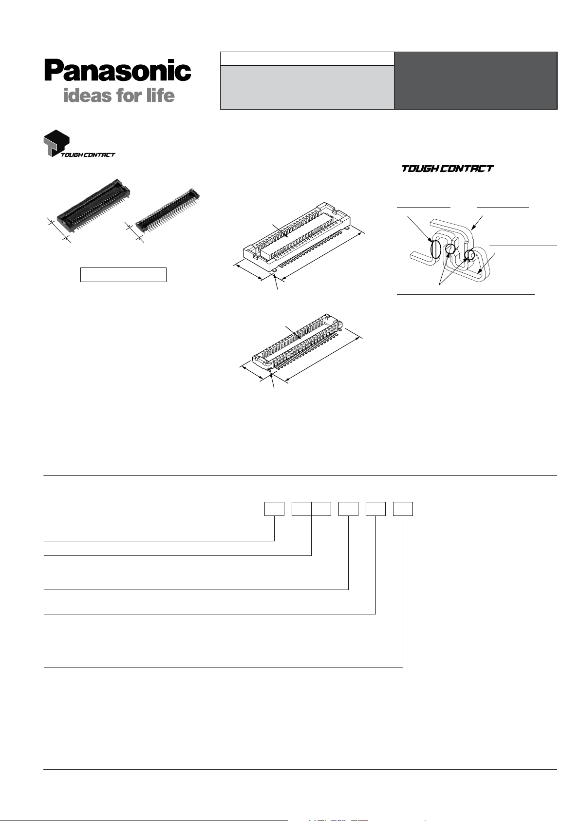
For board-to-FPC
Bellows contact
construction
(Against dropping!)
Ni barrier
construction
(Against solder rise!)
V notch and Double contact constructions
(Against foreign particles and flux!)
Porosity treatment
(Against corrosive gases!)
AXT7, 8
3.4mm
2.6mm
Socket Header
RoHS compliant
Narrow pitch connectors
(0.35mm pitch)
FEATURES
1. Space-saving design (0.35 mm
pitch)
When mated, the footprint is reduced by
approx. 12% from F4S series (40 pin
contacts).
Suction face
0.8mm
3.4 mm
F4S 3.6 mm
Suction face
0.8mm
2.6mm
9.35 mm (40 pin contacts)
F4S 10.50 mm (40 pin contacts)
Soldering terminals
at each corner
8.62 mm (40 pin contacts)
F4S 9.80 mm (40 pin contacts)
Soldering terminals
at each corner
Socket
Header
F35S Series
2. Strong resistance to adverse
environments! Utilizes
“” construction
for high contact reliability.
3. Soldering terminals at each corner
enhance mounting strength.
4. Simple lock structure provides
tactile feedback to ensure excellent
mating/unmating operation feel.
5. Gull-wing-shaped terminals to
facilitate visual inspections.
APPLICATIONS
Ideal for board-to-FPC connections in
mobile equipment that requires size
and thickness reduction and
functionality enhancement.
ORDERING INFORMATION
7: Narrow Pitch Connector F35S (0.35 mm pitch) Socket
8: Narrow Pitch Connector F35S (0.35 mm pitch) Header
Number of pins (2 digits)
Mated height
<Socket> / <Header>
1: For mated height 1.0 mm
Functions
2: Without positioning bosses
Surface treatment (Contact portion / Terminal portion)
<Socket>
4: Base: Ni plating, Surface: Au plating (for Ni barrier available)
<Header>
4: Base: Ni plating, Surface: Au plating
AXT 421
ACCTB27E 201201-T
Panasonic Corporation Automation Controls Business Unit industrial.panasonic.com/ac/e
Page 2
AXT7, 8
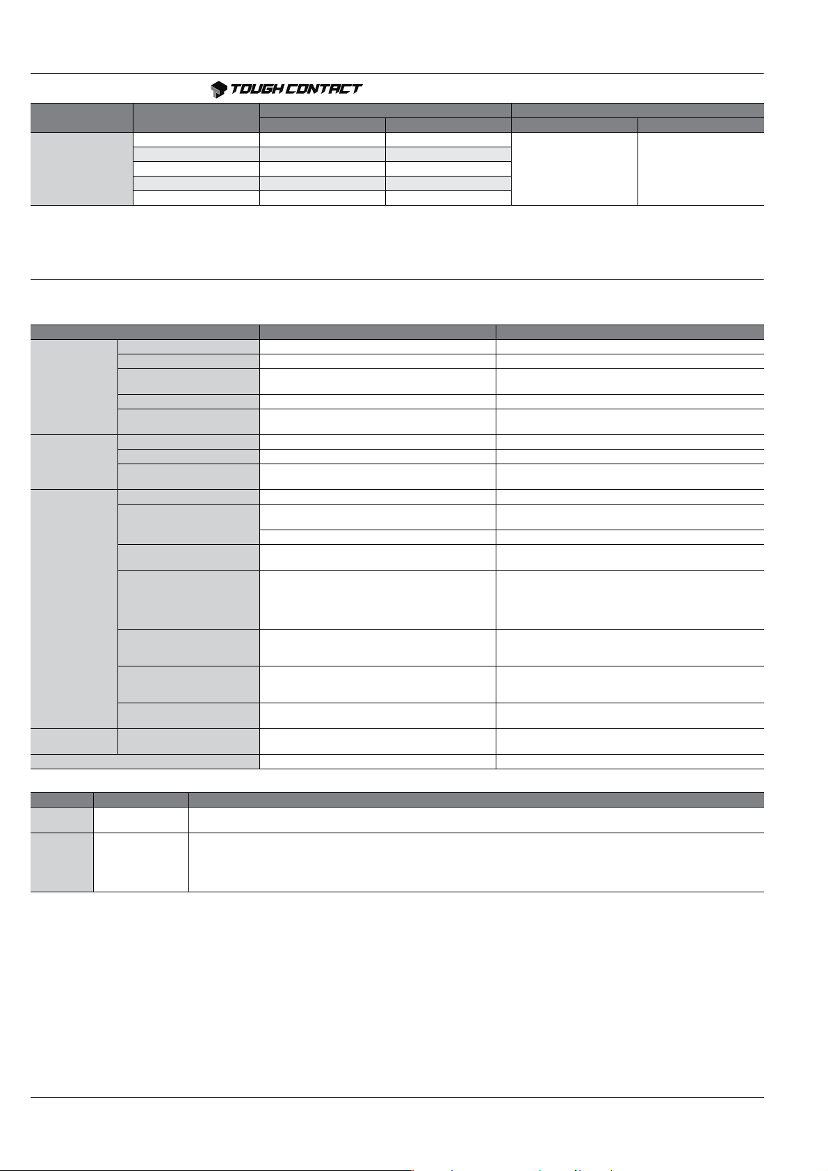
PRODUCT TYPES
Mated height Number of pins
40 AXT740124 AXT840124
50 AXT750124 AXT850124
1.0mm
Notes: 1. Order unit: For volume production: 1-inner-box (1-reel) units
Samples for mounting check: 50-connector units. Please contact our sales office.
2. The abov e part numbers are for connectors without positioning bosses, which are standard. When ordering connectors with positioning bosses, please contact our
sales office.
3. Please contact us for connectors having a number of pins other than those listed above.
60 AXT760124 AXT860124
70 AXT770124 AXT870124
80 AXT780124 AXT880124
Socket Header Inner carton Outer carton
SPECIFICATIONS
1. Characteristics
Item Specifications Conditions
Rated current 0.25A/pin contact (Max. 4 A at total pin contacts)
Rated voltage 60V AC/DC
Electrical
characteristics
Mechanical
characteristics
Environmental
characteristics
Lifetime
characteristics
Unit weight 40 pin contact type: Socket: 0.04 g Header: 0.02 g
2. Material and surface treatment
Part name Material Surface treatment
Molded
portion
Contact and
Post
Breakdown voltage 150V AC for 1 min.
Insulation resistance Min. 1,000MΩ (initial) Using 250V DC megger (applied for 1 min.)
Contact resistance Max. 100mΩ
Composite insertion force Max. 0.981N/pin contacts × pin contacts (initial)
Composite removal force Min. 0.165N/pin contacts × pin contacts
Contact holding force
(Socket contact)
Ambient temperature –55°C to +85°C No freezing at low temperatures. No dew condensation.
Soldering heat resistance
Storage temperature
Thermal shock resistance
(header and socket mated)
Humidity resistance
(header and socket mated)
Saltwater spray resistance
(header and socket mated)
H2S resistance
(header and socket mated)
Insertion and removal life 50 times
LCP resin
(UL94V-0)
Copper alloy
—
Contact portion:
Terminal portion: Base: Ni plating, Surface: Au plating (except the terminal tips)
The socket terminals close to the portion to be soldered have nickel barriers (exposed nickel portions).
Soldering terminals: Sockets: Base: Ni plating, Surface: Pd+Au flash plating (except the terminal tips)
Min. 0.49N/pin contacts
Peak temperature: 260°C or less (on the surface of
the PC board around the connector terminals)
300°C within 5 sec. 350°C within 3 sec. Soldering iron
–55°C to +85°C (product only)
–40°C to +50°C (emboss packing)
5 cycles,
insulation resistance min. 100MΩ,
contact resistance max. 100mΩ
120 hours,
insulation resistance min. 100MΩ,
contact resistance max. 100mΩ
24 hours,
insulation resistance min. 100MΩ,
contact resistance max. 100mΩ
48 hours,
contact resistance max. 100mΩ
Base: Ni plating, Surface: Au plating
Headers: Base: Ni plating, Surface: Au plating (except the terminal tips)
Part number Packing
3,000 pieces 6,000 pieces
No short-circuiting or damage at a detection current of 1 mA
when the specified voltage is applied for one minute.
Based on the contact resistance measurement method
specified by JIS C 5402.
Measuring the maximum force.
As the contact is axially pull out.
Infrared reflow soldering
No freezing at low temperatures. No dew condensation.
Sequence
0
1. –55 °C, 30 minutes
−3
2. ~ , Max. 5 minutes
+3
3. 85 °C, 30 minutes
0
4. ~ , Max. 5 minutes
Bath temperature 40±2°C,
humidity 90 to 95% R.H.
Bath temperature 35±2°C,
saltwater concentration 5±1%
Bath temperature 40±2°C, gas concentration 3±1 ppm,
humidity 75 to 80% R.H.
Repeated insertion and removal speed of max. 200 times/
hours
Panasonic Corporation Automation Controls Business Unit industrial.panasonic.com/ac/e
ACCTB27E 201201-T
Page 3
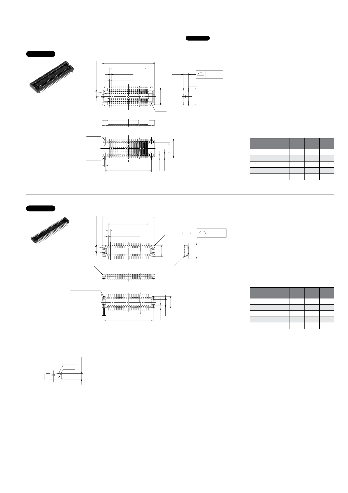
AXT7, 8
DIMENSIONS (Unit: mm)
The CAD data of the products with a CAD Data mark can be downloaded from: http://industrial.panasonic.com/ac/e
Socket (Mated height: 1.0 mm)
CAD Data
A
Y note
Z note
0.80 (Suction face)
0.35±0.05
0.12±0.03
0.30±0.03
B±0.1
C±0.1
3.00
C0.15
0.35
(0.70)
2.00
0.97
3.40
Terminal coplanarity
0.08
(Contact and soldering terminals)
3.40
General tolerance: ±0.2
Note: Since the soldering terminals are built into the body, the sections Y and Z are electrically connected.
Header (Mated height: 1.0 mm)
CAD Data
A
0.80 (Suction face)
B±0.1
0.35±0.05
0.12±0.03
0.83
R 0.15
1.86
Terminal coplanarity
0.08
(Post and soldering terminals)
2.60
Dimension table (mm)
Number of pins/
dimension
40 9.35 6.65 8.25
50 11.10 8.40 10.00
60 12.85 10.15 11.75
70 14.60 11.90 13.50
80 16.35 13.65 15.25
A B C
C 0.13
Soldering terminals
• Socket and Header are mated
Header
Socket
1.00±0.15
0.12±0.03
C±0.1
(0.48)
C 0.13
1.90
Soldering terminals
0.94
General tolerance: ±0.2
Dimension table (mm)
Number of pins/
dimension
40 8.62 6.65 8.05
50 10.37 8.40 9.80
60 12.12 10.15 11.55
70 13.87 11.90 13.30
80 15.62 13.65 15.05
A B C
ACCTB27E 201201-T
Panasonic Corporation Automation Controls Business Unit industrial.panasonic.com/ac/e
Page 4

AXT7, 8
EMBOSSED T APE DIMENSIONS (Unit: mm) (Common to all sockets and headers)
• Specifications for taping
(In accordance with JIS C 0806-1990. However, not applied to
the mounting-hole pitch of some connectors.)
Tape I Tape II
Dimension A: 24 mm or less Dimension A: 32 mm or less
(A±0.3)
(C)
(1.75)
(4.0)
(2.0)
8.0
1.5
+0.1
Leading direction after packaging
0
Leading direction after packaging
dia.
(A±0.3)
(B)
(C)
(1.75)
1.5
(4.0)
(2.0)8.0
+0.1
0
dia.
• Dimension table (Unit: mm)
Type/Mated height Number of pins Type of taping A B C D Quantity per reel
Common for sockets and headers:
1.0mm
40 to 70 Tape I 24.0 — 11.5 25.4 3,000
80 Tape II 32.0 28.4 14.2 33.4 3,000
• Connector orientation with respect to embossed tape feeding direction
Direction
of tape progress
Type
Socket Header
• Specifications for the plastic reel
(In accordance with EIAJET-7200B.)
(D±1)
380 dia.
Common for F35S
Label
Taping reel
Top cover tape
Embossed carrier tape
Embossed mounting-hole
NOTES
1. Design of PC board patterns
Conduct the recommended foot pattern
design, in order to preserve the
mechanical strength of terminal solder
areas.
2. Recommended PC board and metal
mask patterns
Connectors are mounted with high pitch
density, intervals of 0.35 mm, 0.4 mm or
0.5 mm.
In order to reduce solder bridges and
other issues make sure the proper levels
of solder is used.
The figures to the right are recommended
metal mask patterns. Please use them as
a reference.
Note: There is no indication on this product regarding top-bottom or left-right orientation.
• Socket (Mated height: 1.0 mm)
Recommended PC board pattern (TOP VIEW)
0.35±0.03
0.20±0.03
(1.00)
3.80±0.03
1.80±0.03
0.70±0.03
0.80±0.03
Recommended metal mask opening pattern
Metal mask thickness: When 120µm
(Terminal opening ratio: 65%)
(Metal-part opening ratio: 100%)
0.35±0.01
0.18±0.01
(1.00)
1.80±0.01
3.80±0.01
0.70±0.01
0.80±0.01
(0.72)
0.60 or less
: Insulatin
area
(0.52)
2.56±0.01
2.36±0.03
3.60±0.01
• Header (Mated height: 1.0 mm)
Recommended PC board pattern (TOP VIEW)
0.35±0.03
0.20±0.03
2.06±0.03
(0.655)
0.75±0.03
0.45±0.03
Recommended metal mask opening pattern
Metal mask thickness: When 120µm
(Terminal opening ratio: 60%)
(Metal-part opening ratio: 100%)
0.35±0.01
0.18±0.01
(0.655)
0.75±0.01
2.06±0.01
0.45±0.01
0.70±0.01
(0.75)
1.00 or less
1.70±0.03
: Insulation
area
(0.50)
2.00±0.01
3.00±0.01
3.20±0.03
Please refer to the latest product
specifications when designing your
product.
Panasonic Corporation Automation Controls Business Unit industrial.panasonic.com/ac/e
ACCTB27E 201201-T
Page 5

NOTES FOR USING SMD TYPE CONNECTORS (Common)
NO TES FOR USING SMD TYPE CONNECTORS
(Common)
Regarding the design of devices and PC board patterns
1) When connecting several connectors
together by stacking, make sure to
maintain proper accuracy in the design of
structure and mounting equipment so
that the connectors are not subjected to
twisting and torsional forces.
2) With mounting equipment, there may
be up to a ±0.2 to 0.3-mm error in
positioning. Be sure to design PC boards
and patterns while taking into
consideration the performance and
abilities of the required equipment.
3) Some connectors have tabs embossed
on the body to aid in positioning. When
using these connectors, make sure that
the PC board is designed with positioning
holes to match these tabs.
4) To ensure the required mechanical
strength when soldering the connector
terminals, make sure the PC board
meets recommended PC board pattern
design dimensions given.
5) For all connectors of the narrow-pitch
series, to prevent the PC board from
coming off during vibrations or impacts,
and to prevent loads from falling directly
on the soldered portions, be sure to
design some means to fix the PC board
in place.
Example) Secure in place with screws
Screw
Spacer
When connecting PC boards, take
appropriate measures to prevent the
connector from coming off.
6) Notes when using a FPC.
(1) When the connector is soldered to an
FPC board, during its insertion and
removal procedures, forces may be
applied to the terminals and cause the
soldering to come off. It is recommended
to use a reinforcement board on the
backside of the FPC board to which the
connector is being connected. Please
make the reinforcement board
dimensions bigger than the outer limits of
the recommended PC board pattern
(should be approximately 1 mm greater
than the outer limit).
Material should be glass epoxy or
polyimide, and the thickness should be
between 0.2 and 0.3 mm.
(2) Collisions, impacts, or turning of FPC
boards, may apply forces on the
Connector
Spacer
PC board
connector and cause it to come loose.
Therefore, make to design retaining
plates or screws that will fix the connector
in place.
7) The narrow-pitch connector series is
designed to be compact and thin.
Although ease of handling has been
taken into account, take care when
mating the connectors, as displacement
or angled mating could damage or
deform the connector.
Regarding the selection of the connector placement machine and the mounting
procedures
1) Select the placement machine taking
into consideration the connector height,
required positioning accuracy, and
packaging conditions.
2) Be aware that if the catching force of
the placement machine is too great, it
may deform the shape of the connector
body or connector terminals.
3) Be aware that during mounting,
external forces may be applied to the
connector contact surfaces and terminals
and cause deformations.
4) Depending on the size of the
connector being used, self alignment
may not be possible. In such cases, be
sure to carefully position the terminal with
the PC board pattern.
5) The positioning bosses give an
approximate alignment for positioning on
the PC board. F or accur ate positioning of
the connector when mounting it to the PC
board, we recommend using an
automatic positioning machine.
Panasonic Corporation Automation Controls Business Unit industrial.panasonic.com/ac/e
ACCTB10E 201201-T
Page 6

NOTES FOR USING SMD TYPE CONNECTORS (Common)
Regarding soldering
1. Reflow soldering
1) Measure the recommended profile
temperature for reflow soldering by
placing a sensor on the PC board near
the connector surface or terminals. (The
setting for the sensor will differ depending
on the sensor used, so be sure to
carefully read the instructions that comes
with it.)
2) As for cream solder printing, screen
printing is recommended.
3) See the specifications and drawings
for the product in question for the metal
mask pattern diagrams.
4) When mounting on both sides of the
PC board and the connector is mounting
on the underside, use adhesives or other
means to ensure the connector is
properly fixed to the PC board. (Double
reflow soldering on the same side is
possible.)
5) N
2 reflow, conducting reflow soldering
in a nitrogen atmosphere, increases the
solder flow too greatly, enabling wicking
to occur. Make sure that the solder feed
rate and temperature profile are
appropriate.
Soldering conditions
Please use the reflow temperature profile
conditions recommended below for
reflow soldering. Please contact us
before using a temperature profile other
than that described below (e.g. lead-free
solder).
• Narrow-pitch connectors
(except P5 floating and P8 type)
Upper limited (Solder heat resistance)
Temperature
Peak temperature 260°C
• Narrow-pitch connector (P5 floating, P8)
Temperature
245°C max.
155 to 165°C
Lower limited (Solder wettability)
230°C
180°C
150°C
Preheating
60 to 120 sec.
Peak temperature
Preheating
60 to 120 sec.
Peak temperature
220°C
200°C
25 sec.
70 sec.
Time
200°C
Within 30 sec.
Time
For products other than the ones above,
please refer to the latest product
specifications.
6) The temperatures are measured at the
surface of the PC board near the
connector terminals. (The setting for the
sensor will differ depending on the sensor
used, so be sure to carefully read the
instructions that comes with it.)
7) The temperature profiles given in this
catalog are values measured when using
the connector on a resin-based PC
board. When performed reflow soldering
on a metal board (iron, aluminum, etc.) or
a metal table to mount on a FPC, make
sure there is no deformation or
discoloration of the connector beforehand
and then begin mounting.
2. Hand soldering
1) Set the soldering iron so that the tip
temperature is less than that given in the
table below.
Table A
Product name Soldering iron temperature
SMD type connectors
300°C within 5 sec.
350°C within 3 sec.
2) Do not allow flux to spread onto the
connector leads or PC board. This may
lead to flux rising up to the connector
inside.
3) Touch the soldering iron to the foot
pattern. After the foot pattern and
connector terminal are heated, apply the
solder wire so it melts at the end of the
connector terminals.
Apply the solder
wire here
Terminal
Pattern
Soldering
PC board
iron
Small angle as
possible up to
45 degrees
4) Be aware that soldering while applying
a load on the connector terminals may
cause improper operation of the
connector.
5) Thoroughly clean the soldering iron.
6) Flux from the solder wire may get on
the contact surfaces during soldering
operations. After soldering, carefully
check the contact surfaces and clean off
any solder before use.
7) For soldering of prototype devices
during product development, you can
perform soldering at the necessary
locations by heating with a hot-air gun by
applying cream solder to the foot pattern
beforehand. However, at this time, make
sure that the air pressure does not move
connectors by carefully holding them
down with tweezers or other similar tool.
Also, be careful not to go too close to the
connectors and melt any of the molded
components.
3. Solder reworking
1) Finish reworking in one operation.
2) For reworking of the solder bridge, use
a soldering iron with a flat tip. To prevent
flux from climbing up to the contact
surfaces, do not add more flux.
3) Keep the soldering iron tip temperature
below the temperature given in Table A.
ACCTB10E 201201-T
Panasonic Corporation Automation Controls Business Unit industrial.panasonic.com/ac/e
Page 7

NOTES FOR USING SMD TYPE CONNECTORS (Common)
Handling Single
Components
1) Make sure not to drop or allow parts to
fall from work bench
2) Excessive force applied to the
terminals could cause warping, come
out, or weaken the adhesive strength of
the solder. Handle with care.
3) Repeated bending of the terminals
may cause terminals to break.
4) Do not use alcohol for cleaning. Doing
so may whiten the surface of molded
parts.
Storage of connectors
1) To prevent problems from voids or air
pockets due to heat of reflow soldering,
avoid storing the connectors in areas of
high humidity. When storing the
connectors for more than six months, be
sure to consider storage area where the
humidity is properly controlled.
2) Depending on the connector type, the
color of the connector may vary from
connector to connector depending on
when it is produced.
Cleaning flux from PC board
1) To increase the cleanliness of the
cleaning fluid and cleaning operations,
prepare equipment for cleaning process
beginning with boil cleaning, ultrasonic
cleaning, and then vapor cleaning.
2) Carefully oversee the cleanliness of
the cleaning fluids to make sure that the
contact surfaces do not become dirty
from the cleaning fluid itself.
3) Since some powerful cleaning
solutions may dissolve molded
components of the connector and wipe
off or discolor printed letters, we
recommend aqua pura electronic parts
cleaners. Please consult us if y ou wish to
use other types of cleaning fluids.
4) Please note that the surfaces of
molded parts may whiten when cleaned
with alcohol.
Some connectors may change color
slightly if subjected to ultraviolet rays
during storage. This is normal and will not
affect the operation of the connector.
3) When storing the connectors with the
PC boards assembled and components
alreeady set, be careful not to stack them
up so the connectors are subjected to
excessive forces.
Handling the PC board
• Handling the PC board after
mounting the connector
When cutting or bending the PC board
after mounting the connector, be careful
that the soldered sections are subjected
to excessive forces.
The soldered areas should not be subjected to forces.
4) Avoid storing the connectors in
locations with excessive dust. The dust
may accumulate and cause improper
connections at the contact surfaces.
Other Notes
1) These products are made for the
design of compact and lightweight
devices and therefore the thic kness of the
molded components has been made very
thin. Therefore, be careful during
insertion and removal operations for
excessive forces applied may damage
the products.
2) Dropping of the products or rough
mishandling may bend or damage the
terminals and possibly hinder proper
reflow soldering.
3) Before soldering, try not to insert or
remove the connector more than
absolutely necessary.
4) When coating the PC board after
soldering the connector to prevent the
deterioration of insulation, perform the
coating in such a way so that the coating
does not get on the connector.
5) There may be variations in the colors
of products from different production lots.
This is normal.
Regarding sample orders to confirm proper mounting
When ordering samples to confirm
proper mounting with the placement
machine, connectors are delivered in 50piece units in the condition given right.
Consult a sale representative for ordering
sample units.
Condition when delivered from manufacturing
Reel
Embossed tape
amount required for
the mounting
Required number
of products for
sample production
(Unit 50 pcs.)
(Delivery can also be made on a reel by
customer request.)
6) The connectors are not meant to be
used for switching.
7) Be sure not to allow external pressure
to act on connectors when assembling
PCBs or moving in block assemblies.
Please refer to the latest product
specifications when designing your
product.
Panasonic Corporation Automation Controls Business Unit industrial.panasonic.com/ac/e
ACCTB10E 201201-T
 Loading...