

Page 1
ORDER No.AED02110467
AUTOMOTIVE ELECTRONICS
GM
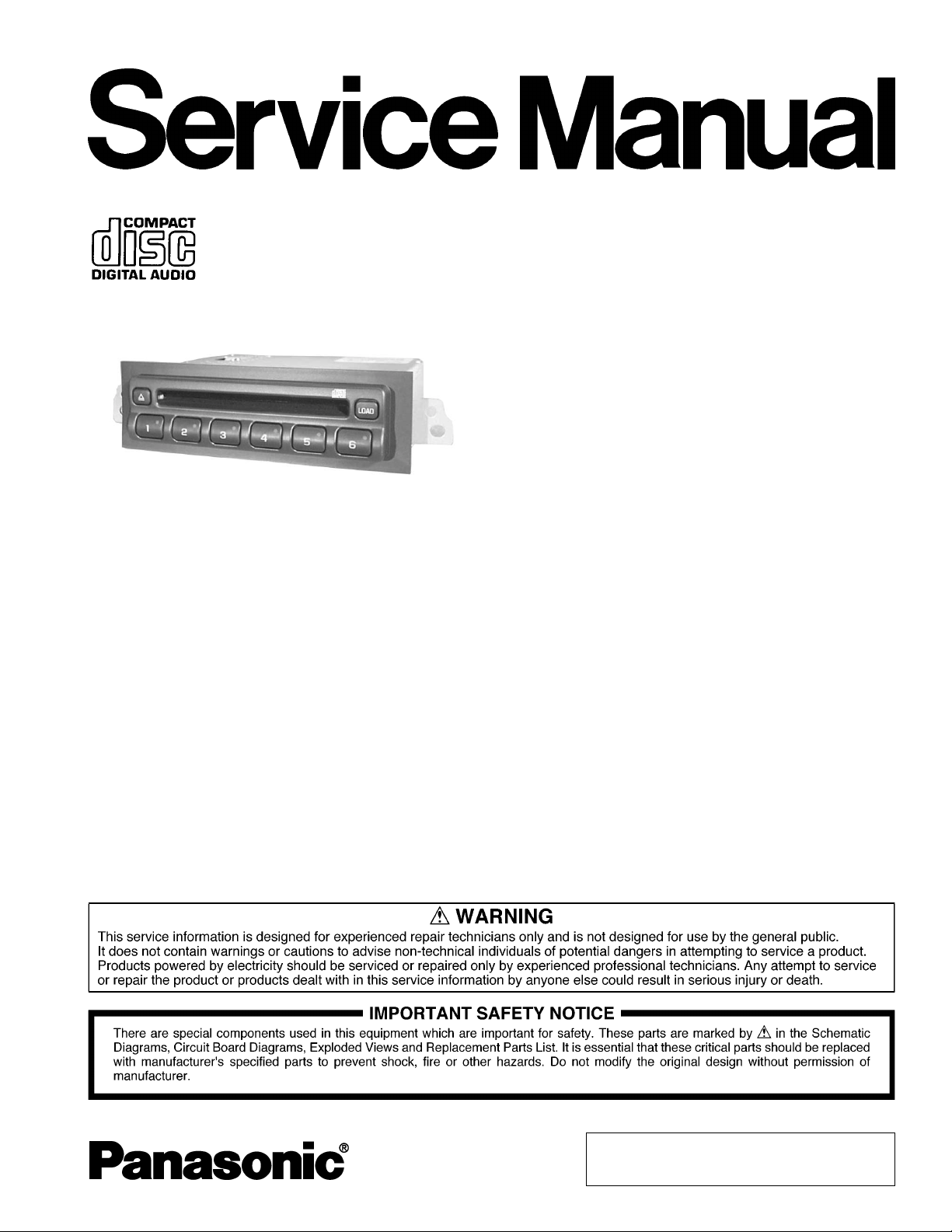
CX-CG0260Z
6-Disc In-Dash CD Changer
GM PART No. :15055250
VEHICLE : Denali/ GMT820D
Grand Surb/ GMT
Escalade/ GMT820C
Cadillac/ GMT806
DESTINATION : North America
PRODUCED AFTER: Jan., 2002
I0
Specifications*
General
Power Supply DC 12V (11V - 16V)
Test Voltage 13.2V
Negative ground
Current Consumption Less than 1.0A
Output Level 1.25Vrms
Channel Separation 65dB min. (at 100kΩ Load)
Cannel Balance 1.0dB max. (at 1kHz)
Signal to Noise Ratio 75dB min.
THD 0.1% max. (at 1kHz)
Dimensions** (W×H×D) 178 × 50 × 177.5 (mm)
(not including connector protrusion or
brackets)
Weight** 2.0kg
* Specifications and the design are subject to possible modification
without notice due to improvements.
** Dimensions and Weight shown are approximate.
•
• Above specifications comply with EIA standards.
• •
© 2002 Matsushita Communication Industrial Co.,
Ltd. All rights reserved. Unauthorized copying and
distribution is a violation of law.
Page 2
GM / CX-CG0260Z
CONTENTS
Page Page
1 FEATUERS 2
2 LASER PRODUCTS
3 REAR VIEW AND CONNECTORS
4 FRONT VIEW AND FUNCTIONS
5 WIRING CONNECTIONS
6 BLOCK DIAGRAM
7 TERMINALS DESCRIPTION
8 CD DISC CENTERING ALIGNMENT
9 PACKAGE AND IC BLOCK DIAGRAM
10 REPLACEM ENT PARTS LIST 13
2
11 EXPLODED VIEW (Unit)
3
12 CD CHANGER PARTS LIST
13 EXPLODE D VIEW (CD Deck-1)
3
4
14 EXPLODE D VIEW (CD Deck-2)
5
15 EXPLODE D VIEW (CD Deck-3)
16 WIRING DIAGRAM
7
9
17 SCHEMAT IC DIAGRAM
10
1 FEATUERS
•
•
6-Disc CD changer capacity
• •
•
•
1 DIN size.
• •
•
•
Includes Illumination circuit to improve neght visibility.
• •
16
17
20
21
22
23
27
2 LASER PRODUCTS
2
Page 3
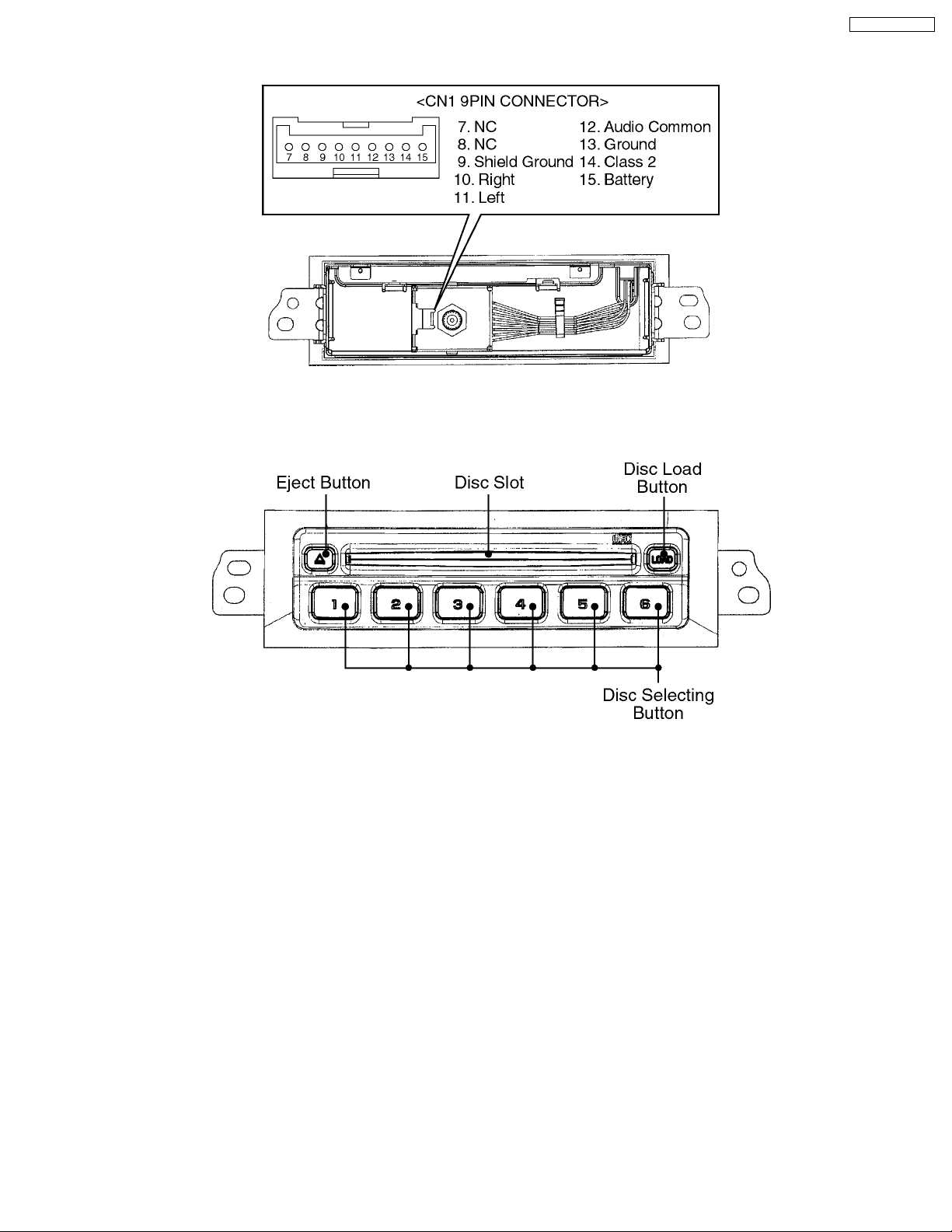
3 REAR VIEW AND CONNECTORS
4 FRONT VIEW AND FUNCTIONS
GM / CX-CG0260Z
3
Page 4
GM / CX-CG0260Z
5 WIRING CONNECTIONS
4
Page 5
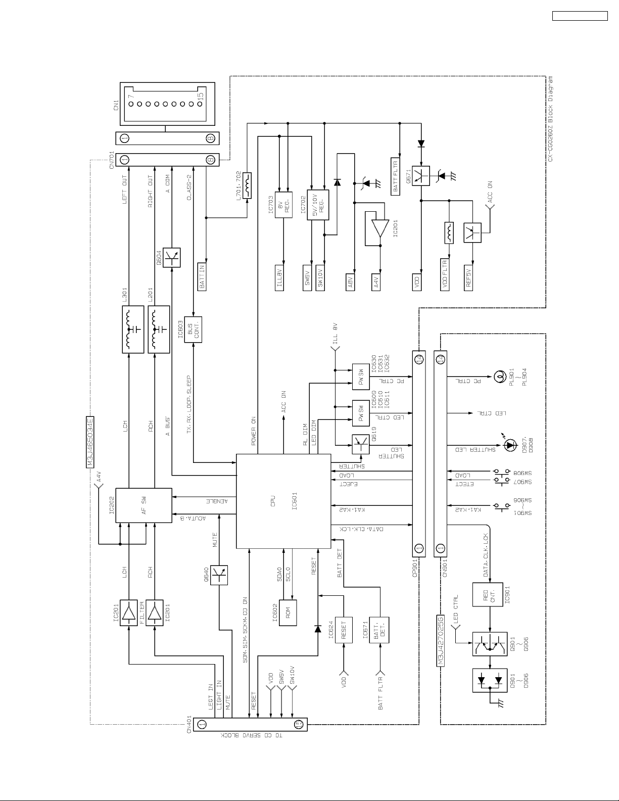
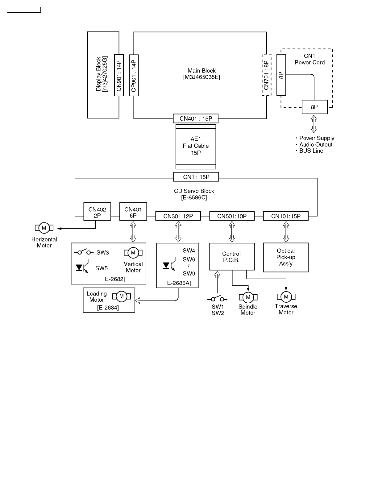
6 BLOCK DIAGRAM
6.1. Main/ Display Block
GM / CX-CG0260Z
5
Page 6
GM / CX-CG0260Z
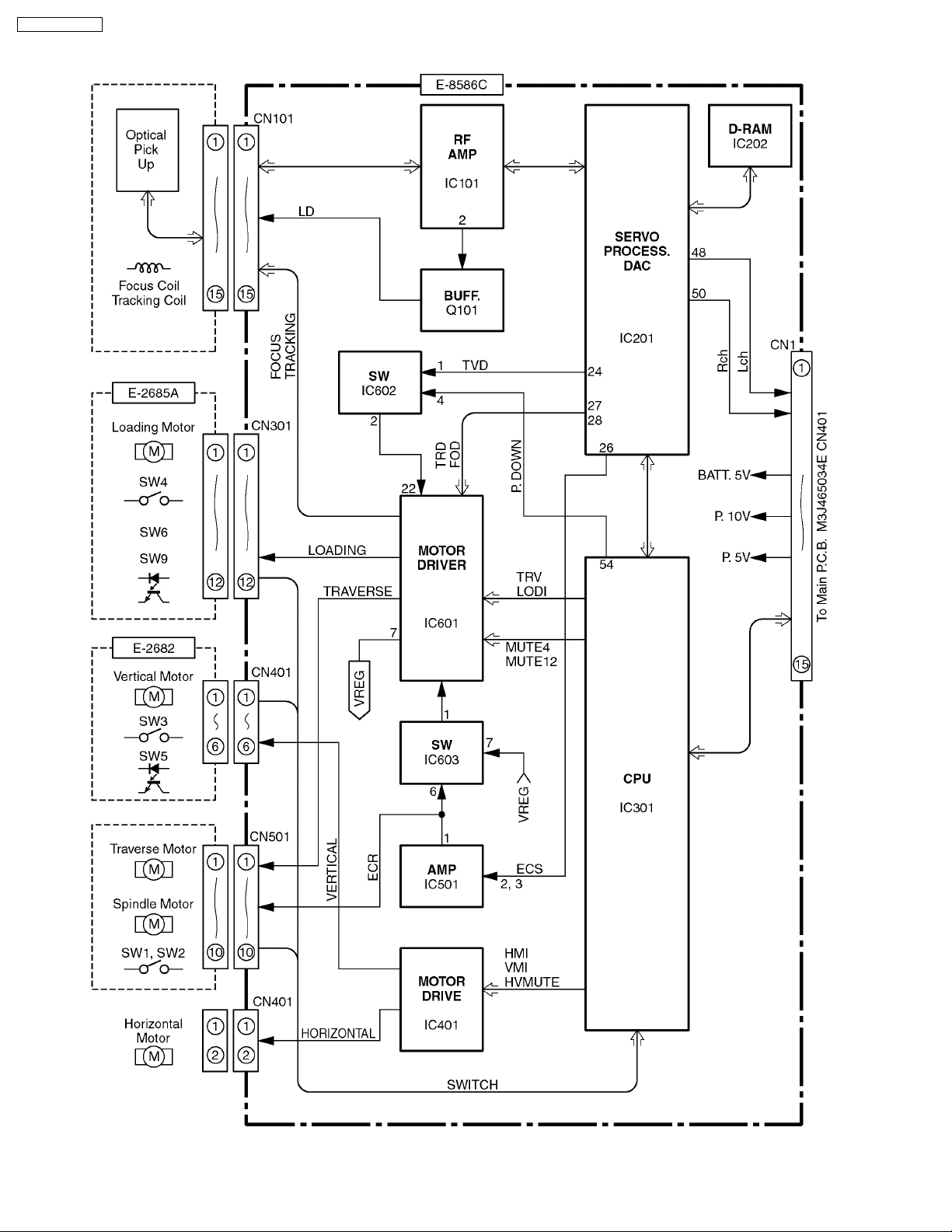
6.2. CD Servo Block
6
Page 7
7 TERMINALS DESCRIPTION
GM / CX-CG0260Z
7.1. Main Block
IC601 : UC2BBGF00008
Pin No. Port Description I/O
1 (NC) - 2 SDA Serial Data I/O
3 SCL Clock for serial data O
4 (NC) - 5 (NC) - 6 (NC) - 7 BATT DET Battery Voltage Detection I
8 RD ON (+5V pull up) -
9 EJECT EJECT Switch signal I
10 LOAD LOAD Switch signal I
11 AVREF1 +5V power supply 12 K2A Key Switch signal 2 I
13 K1A Key Switch signal 1 I
14 (NC) - 15 (NC) - 16 (NC) - 17 (NC) - 18 (NC) - 19 (NC) - 20 AVSS Ground 21 (NC) - 22 A BUS A BUS out O
23 ACC ON ACC On signal O
24 (NC) - 25 (NC) - 26 (NC) - 27 RESET Reset input I
28 CD ON CD On signal O
29 SOM CD changer serial data I
30 SIM CD changer serial data O
31 SCKM Clock for serial data O
32 VDD +5V power supply 33 VSS Ground 34 SMUTTER Shatter LED O
35 (NC) - 36 (NC) - 37 (NC) - 38 (NC) - 39 (NC) - 40 (NC) - 41 ACNTA Audio switch control A O
42 ACNTB Audio switch control B O
43 AENBL Audio switch enable O
44 POWER ON Power On signal O
45 LCK LED Driver LCK O
46 (NC) - 47 DATA LED Driver data O
48 CLK LED Driver clock O
49 (NC) - 50 (NC) - 51 (NC) - 52 (NC) - 53 (NC) - 54 (NC) - 55 (NC) - 56 LED DIM LED dimer signal O
57 PL DIM Pilot Lamp dimmer control O
58 (NC) - 59 (NC) - 60 SLEEP Class2 transeiver sleep O
61 LOOP Class2 transeiver loop O
Pin No. Port Description I/O
62 C2RX Class2 transeiver RX I
63 C2TX Class2 transeiver TX O
64 RESET Reset input I
65 IC(VPP) (TP1) #REF!
66 X2 Crystal osillator 67 X1 Crystal osillator 68 VSS1 Ground 69 VDD1 +5V power supply 70 VDD0 +5V power supply 71 AVREF0 +5V power supply 72 (NC) - 73 (NC) - 74 (NC) - 75 (NC) - 76 (NC) - 77 (NC) - 78 (NC) - 79 (NC) - 80 AVSS1 Ground -
Note :
Voltage measuerments are with respect to ground, with a
voltmeter (Internal resistance : 10M ohms.)
7.2. CD Servo Block
IC201 : MN662783RPW
Pin No. Port Description I/O (V)
1 VDD +5V power supply - 5.0
2 D0 D-RAM data I/O 2.3
3 D1 D-RAM data I/O 1.8
4 /WE D-RAM data write O 4.9
5 /RAS D-RAM row address strobe O 3.4
6 D2 D-RAM data I/O 0.8
7 D3 D-RAM data I/O 0
8 /CAS0 D-RAM columun address strobe O 3.9
9 /CAS1 D-RAM columun address strobe O 0
10 A8 D-RAM address O 0.6
11 A7 D-RAM address O 1.1
12 A6 D-RAM address O 0.7
13 A5 D-RAM address O 0
14 A4 D-RAM address O 1.1
15 A9 D-RAM address O 0.4
16 A0 D-RAM address O 1.0
17 A1 D-RAM address O 1.0
18 A2 D-RAM address O 1.0
19 A3 D-RAM address O 0
20 VSS2 Ground - 0
21 VDD2 +5V power supply - 5.0
22, 23 - Not used - -
24 TVD Traverse motor control O 2.5
25 PC Not used - 26 ECS Spindle motor control O 2.4
27 TRD Tracking coil drive O 2.5
28 FOD Focus coil drive O 2.4
29 FBAL Focus balance O 1.9
30 TBAL Tracking balance O 3.0
31 VREF Reference voltage I 2.5
32 FE Focus error I 2.5
33 TE Tracking error I 2.5
34 RFENV RF envelope I 2.5
35 OFT Off track signal I 0
36 /RFDET RF detecting signal I 0
7
Page 8

GM / CX-CG0260Z
37 BDO Drop-out signal I 0
38 LDON Laser on signal O 4.5
39 ARF RF signal I 2.5
40 IREF Reference current input I 1.2
41 DRF Biase for DSL I 2.4
42 DSLF Loop filter for DSL I/O 2.5
43 SDLF2 Loop filter for DSL I/O 2.2
44 PLLF Loop filter for PLL I/O 1.4
45 VCOF Not used - 46 AVDD2 +5V power supply - 5.0
47 AVSS2 Ground - 0
48 OUTL L channel output O 2.3
49 AVSS1 Ground - 0
50 OUTR R channel output O 2.3
51 AVDD1 +5V power supply - 4.7
52-54 - (Connecting to ground) - 0
55 FLAG Flag output O 0
56 FCLK Frame clock O 0
57-59 - Not used - -
60 TX Not used - 61 MCLK Clock for I/F command I 1.0
62 MDATA Data for I/F command I 3.1
63 MLD I/F command load I 5.0
64 BLKCK Subcode block clock O 0
65 SQCK Ext. clock for sub code-Q I 5.0
66 SUBQ Code for sub. code-Q O 3.8
67 DMUTE Mute input I 0
68 STAT Status signal O 5.0
69 /RST Reset input I 5.0
70 CSEL (Connecting to ground) - 0
71 PMCK PM clock O 2.5
72 SMCK SM clock O 2.5
73 SUBC Serial data of sub code O 0
74 SBCK Shift clock for SUBC I 0.6
75 /CLDCK Not used - 76 /TEST (Connecting to VDD) - 5.0
77 X1 Crystal oscillator - 0.4
78 X2 Crystal oscillator - 3.2
79 VDD1 +5V power supply - 5.0
80 VSS1 Ground - 0
24 SUBQ Code for sub. code-Q I 1.6
25 - Not used - 5.0
26 - (Ground pull-down) - 0
27 CD.ON CD changer start/stop I 5.0
28 - Not used - 5.0
29 BLKCK Sub. code block clock I 0
30 P.ON Not used - 5.0
31 MUTE Mute output O 5.0
32 - (Ground pull-down) - 0
33 SENS Servo status O 0
34 CLVS Servo status O 5.0
35 FLOCK Focus servo lock O 0.2
36 TLOCK Tracking servo lock O 0
37 VMI Horizontal motor control O 2.5
38 HMI Vertical motor control O 0
39 HVMUTE H/V motor mute O 0
40-42 - (Ground pull-down) - 0
43 SW9 Disc-in (B) SW I 0
44 SW8 Disc-in (L) SW I 0
45 SW7 Disc-in (F) SW I 0
46 SW6 Disc push SW I 0
47 SW5 Tray hight SW I 4.5
48 BDO Drop-out signal I 0
49 DQSY Not used - 50 /RST Reset output O 5.0
51 STAT Status signal I 2.1
52 DMUTE Mute output O 0
53 XE Not used - 54 P.DOWN Power down signal O 0
55 - No connection - 56 MLD I/F command load O 5.0
57 MDATA Data for I/F command O 3.1
58 MCLK Clock for I/F command O 4.1
59 SPMT Spindle mute O 5.0
60 MUTE12 Focus/Tracking mute O 0
61 MUTE4 Loading motor mute O 4.8
62 LDOI Loading motor control I/O 2.5
63 TRV Forced traverse control I/O 2.4
64 SYNC Not used - -
IC301 : MN1873260AB4
Pin
No.
1 VDD +5V power supply - 5.0
2 OSC2 Crystal oscillator - 2.2
3 OSC1 Crystal oscillator - 2.1
4 VSS Ground - 0
5 XI (Connecting to ground) - 0
6 XO Not used - 7 CM (Connecting to ground) - 0
8 VREFH Reference voltage I 5.0
9 SW13 Shuter SW I 4.9
10 SW12 Horizontal origin I 4.9
11 SW11 Clump SW I 0
12 SW10 Play SW I 0
13 SW4 Shuter SW I 4.9
14 SW3 Tray origin SW I 0
15 SW2 Inner SW I 4.8
16 SW1 Outer SW I 4.9
17 VREFL Reference voltage I 0
18 /RESET Reset input I 4.9
19 - (Ground pull-down) - 0
20 SCKM Clock for serial data I 5.0
21 SIM CD changer serial data I 1.3
22 SOM CD changer serial data O 4.3
23 SQCK Ext. clock for sub. code-Q O 5.0
Port Description I/O (V)
8
Page 9
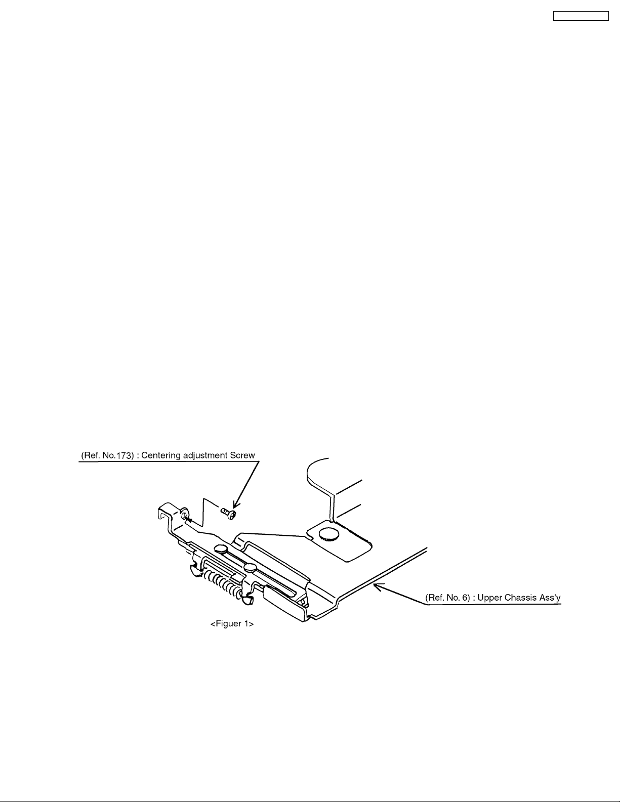
8 CD DISC CENTERING ALIGNMENT
•
•
This adjustment is for assuring that compact discs will be placed in the center of the turntable.
• •
<Adjustment Condition / Jig>
•
•
Power Supply Voltage : 13.2V
• •
•
•
Test Disc : TCD-792A
• •
<Adjustment Procedures>
1. Attach the adjusting screw to the upper chassis (See Figure 1.).
2. Insert the test CD (TCD-792A) into the disc No.1 position and play it.
3. After checking whether the disc is centered on the turntable, turn the adjusting screw unit it is in the center.
<Check Items>
•
•
Check that the disc is correctly centered.
• •
•
•
Check that the disc is securely clamped.
• •
•
•
Check that no abnormal noise is produced when clamping the disc.
• •
GM / CX-CG0260Z
[Directions of Turning the Adjusting Screw]
•
•
CD stops before its proper position : Turn the screw counterclockwise.
• •
•
•
CD overruns : Turn the screw clockwise.
• •
4. After the adjustment, lock the screw.
9
Page 10

GM / CX-CG0260Z
9 PACKAGE AND IC BLOCK DIAGRAM
9.1. Main / Display Block
IC201 YEAMPC4574E1
IC702 YEAM61W12ST
IC202 YEAMPD4052E1
IC604, 671 MN1382QTX
IC901 BU2092FV
10
Page 11

9.2. CD Servo Block
GM / CX-CG0260Z
IC603 : YEAMT4W53FUL
IC101 : C1BB00000173
IC202 : C3ABMB000010
IC401 : YEAMBA6792FY
11
Page 12

GM / CX-CG0260Z
IC601 : C0GBY0000004
IC501 : YEAMPC358G2T
12
Page 13

10 REPLACEMENT PARTS
LIST
Notes :
1. Be sure to make your orders of replacement parts
according to this list.
2. Important safety notice: Components, identified by
mark have special characteristics important for safety.
When replacing any of these components, use only
manufacturer´s specified parts.
3. Location keys in the remarks column indicates the general
location of the parts shown in the exploded drawing, as in a
road map.
4. The marking (RTL) indicates that Retention Time is limited
for this item. After the discontinuation of assembly in
production, the item will continue to be available for a
specific period of time. The retention period of availability is
dependent on the type of assembly, and in accordance with
the laws governing part and product retention. After the end
of this period, the assembly will no longer be available.
5. "MCC" marks in remarkscolumn are indicated supply parts
of Matsushita Communication Industrial Corp. of America
(MCC).
Ref.
No.
[M3J465034E] Main Block
IC´s and TRANSISTORs
IC201 YEAMPC4574E1 IC
IC202 YEAMPD4052E1 IC MCC
IC601 UC2BBGF00008 IC, CPU MCC
IC602 UC3EBE000001 IC MCC
IC603 MC33390 IC MCC
IC604 MN1382QTX IC
IC671 MN1382QTX IC
IC702 YEAMA61W12ST IC, REG
IC703 YEAMBA09ST IC, REG MCC
Q604 2SD1382STTX Transistor
Q609 B1GBCFJN0005 Transistor
Q610 2SB1440TX Transistor
Q611 2SD1030TX Transistor
Q619 B1GDCFJN0005 Transistor
Q629 B1GDCFJN0005 Transistor
Q630 B1GBCFJN0005 Transistor
Q631 2SB1440TX Transistor
Q632 2SD1030TX Transistor
Q671 YEANC3618 Transistor
DIODEs
D601 UJ0LB0000001 Diode, Surge Protect MCC
D606 MA151KTX Diode
D671 YEADRD56M2T1 Diode, Zenner
D672 MA8051HTX Diode, Zenner MCC
D673 MA151KTX Diode
D674 MA151KTX Diode
D701 YEAD30D2FC6 Diode
D702 YEADDSA3A2B Diode
D703 YEADRD82M2T1 Diode, Zenner
D704 MA151KTX Diode
D705 MA151KTX Diode
CAPACITORs
C201 EEVMC1C100R Electrolytic, 10µF 16WV
C202 YECUS1H392KX Ceramic, 3900pF 50WV
C203 YECUS1H682KX Ceramic, 6800pF 50WV
C204 F1J1H182A509 Ceramic, 1800pF 50WV
C205 EEVMC1C100R Electrolytic, 10µF 16WV
Part No. Part Name & Description Remarks
Ref.
No.
C206 EEVMC1C220R Electrolytic, 22µ:F 16WV
C213 YECUS1H102KX Ceramic, 1000pF 50WV
C301 EEVMC1C100R Electrolytic, 10µF 16WV
C302 YECUS1H392KX Ceramic, 3900pF 50WV
C303 YECUS1H682KX Ceramic, 6800pF 50WV
C304 F1J1H182A509 Ceramic, 1800pF 50WV
C305 EEVMC1C100R Electrolytic, 10µF 16WV
C306 EEVMC1C220R Electrolytic, 22µ:F 16WV
;
C313 YECUS1H102KX Ceramic, 1000pF 50WV
C602 YECUS1H221JM Ceramic, 220pF 50WV
C603 YECUS1C104KX Ceramic, 0.1µF 16WV
C604 YECUS1C104KX Ceramic, 0.1µF 16WV
C605 YECUS1H101JM Ceramic, 100pF 50WV
C609 YECUS1C104KX Ceramic, 0.1µF 16WV
C610 YECUS1C104KX Ceramic, 0.1µF 16WV
C611 F1H1H1020001 Ceramic, 1000pF 50WV
C612 F1H1H101A231 Ceramic, 100pF 50WV
C613 F1H1H680A231 Ceramic, 68pF 50WV
C614 F1H1H680A231 Ceramic, 68pF 50WV
C615 F1H1H680A231 Ceramic, 68pF 50WV
C620 YECUS1H103KX Ceramic, 0.01µF 50WV
C621 YECUS1H103KX Ceramic, 0.01µF 50WV
C622 F1J1C1050016 Ceramic, 1µF 16WV MCC
C624 F1J1C1050016 Ceramic, 1µF 16WV MCC
C627 F1J1C1050016 Ceramic, 1µF 16WV MCC
C629 F1J1C1050016 Ceramic, 1µF 16WV MCC
C630 YECUS1H102KX Ceramic, 1000pF 50WV
C671 F1H1C1040002 Ceramic, 0.1µF 16WV
C672 EEVMC1C470P Electrolytic, 47µF 16WV
C673 EEVMC1C470P Electrolytic, 47µF 16WV
C674 YECUS1H104KX Ceramic, 0.1µF 50WV
C675 YECUS1H103KX Ceramic, 0.01µF 50WV
C680 YECUS1H104KX Ceramic, 0.1µF 50WV
C681 F1J1C224A006 Ceramic, 0.22µF 16WV
C682 F1J1C224A006 Ceramic, 0.22µF 16WV
C683 YECUS1H103KX Ceramic, 0.01µF 50WV
C684 YECUS1H104KX Ceramic, 0.1µF 50WV
C705 EEVHA1C331P Electrolytic, 330µF 16WV MCC
C706 EEVFC1C101P Electrolytic, 100µF 16WV
C707 YECUS1H104KX Ceramic, 0.1µF 50WV
C708 EEVMC1C220R Electrolytic, 22µ:F 16WV
C710 YECUS1H104KX Ceramic, 0.1µF 50WV
C711 EEVMC1C470P Electrolytic, 47µF 16WV
C713 EEVMC1C470P Electrolytic, 47µF 16WV
C714 YECUS1H104KX Ceramic, 0.1µF 50WV
C718 YECUS1H104KX Ceramic, 0.1µF 50WV
C723 YECUS1H104KX Ceramic, 0.1µF 50WV
C726 EEVMC1C220R Electrolytic, 22µ:F 16WV
C727 EEVMC0J101P Electrolytic, 100µF 6.3WV
C728 EEVHA1C331P Electrolytic, 330µF 16WV MCC
C751 YECUS1H103KX Ceramic, 0.01µF 50WV
C752 YECUS1H103KX Ceramic, 0.01µF 50WV
C797 EEVHA1C331P Electrolytic, 330µF 16WV MCC
C798 EEVHA1C331P Electrolytic, 330µF 16WV MCC
C799 EEVMC1C470P Electrolytic, 47µF 16WV
COILs
L201 YECCL60R471T Coil
L301 YECCL60R471T Coil
L601 YELT03N470JT Coil
L602 YELTBLM21A10 Coil
L701 YETQ012G157 Coil
L702 YECCL60R471T Coil
RESISTORs
R201 ERJ6GEYJ101V Chip, 100
R202 ERJ6GEYJ102V Chip, 1k
R203 ERJ6GEYJ333V Chip, 33k
R204 ERJ6GEYJ102V Chip, 1k
R205 ERJ6GEYJ102V Chip, 1k
R207 ERJ6GEYJ474V Chip, 470k
Part No. Part Name & Description Remarks
ΩΩΩΩ
1/10W
ΩΩΩΩ
1/10W
ΩΩΩΩ
1/10W
ΩΩΩΩ
1/10W
ΩΩΩΩ
1/10W
ΩΩΩΩ
1/10W
GM / CX-CG0260Z
13
Page 14

GM / CX-CG0260Z
Ref.
No.
R208 ERJ6GEYJ474V Chip, 470k
R209 ERJ6GEYJ103V Chip, 10k
R210 ERJ6GEYJ152V Chip, 1.5k
R301 ERJ6GEYJ101V Chip, 100
R302 ERJ6GEYJ102V Chip, 1k
R303 ERJ6GEYJ333V Chip, 33k
R304 ERJ6GEYJ102V Chip, 1k
R305 ERJ6GEYJ102V Chip, 1k
R307 ERJ6GEYJ474V Chip, 470k
R308 ERJ6GEYJ474V Chip, 470k
R309 ERJ6GEYJ103V Chip, 10k
R310 ERJ6GEYJ152V Chip, 1.5k
R601 ERJ3EKF3401V Chip, 3.4k
R602 ERJ3EKF3401V Chip, 3.4k
R607 ERJ6GEYJ472V Chip, 4.7k
R608 ERJ6GEYJ474V Chip, 470k
R609 ERJ6GEYJ182V Chip, 1.8k
R614 ERJ6GEYJ102V Chip, 1k
R621 ERJ6EKF1072V Chip, 10.7k
R623 ERJ6GEYJ223V Chip, 22k
R624 ERJ6GEYJ223V Chip, 22k
R625 ERJ6GEYJ223V Chip, 22k
R629 ERJ3GEYJ103V Chip, 10k
R631 ERJ6GEY0R00V Chip, 0
R632 ERJ6GEY0R00V Chip, 0
R633 ERJ6GEY0R00V Chip, 0
R634 ERJ6GEYJ104V Chip, 100k
R635 ERJ6GEYJ104V Chip, 100k
R637 ERJ3GEYJ103V Chip, 10k
R638 ERJ3GEYJ473V Chip, 47k
R639 ERJ3GEYJ103V Chip, 10k
R640 ERJ3GEYJ153V Chip, 15k
R641 ERJ3GEYJ103V Chip, 10k
R642 ERJ3GEYJ103V Chip, 10k
R671 ERJ6GEYJ473V Chip, 47k
R674 ERJ6GEYJ563V Chip, 56k
R675 ERJ6GEYJ100V Chip, 10
R676 ERJ6GEYJ473V Chip, 47k
R678 ERJ6GEYJ474V Chip, 470k
R679 ERJ6GEYJ474V Chip, 470k
R707 ERJ6GEYJ680V Chip, 68
R708 ERJ6GEYJ103V Chip, 10k
R709 ERJ6GEYJ103V Chip, 10k
R710 ERJ6GEY0R00V Chip, 0
R711 ERJ6GEY0R00V Chip, 0
R712 ERJ6GEY0R00V Chip, 0
R713 ERJ6GEYJ101V Chip, 100
RESISTOR NETWORKs
R626 EXBV8V102JV Resistor Network, 1k
R627 EXBV8V102JV Resistor Network, 1k
R628 EXBV8V102JV Resistor Network, 1k
R630 EXBV8V102JV Resistor Network, 1k
Part No. Part Name & Description Remarks
ΩΩΩΩ
1/10W
ΩΩΩΩ
1/10W
ΩΩΩΩ
1/10W
ΩΩΩΩ
1/10W
ΩΩΩΩ
1/10W
ΩΩΩΩ
1/10W
ΩΩΩΩ
1/10W
ΩΩΩΩ
1/10W
ΩΩΩΩ
1/10W
ΩΩΩΩ
1/10W
ΩΩΩΩ
1/10W
ΩΩΩΩ
1/10W
ΩΩΩΩ
1/16W MCC
ΩΩΩΩ
1/16W MCC
ΩΩΩΩ
1/10W
ΩΩΩΩ
1/10W
ΩΩΩΩ
1/10W
ΩΩΩΩ
1/10W
ΩΩΩΩ
1/16W MCC
ΩΩΩΩ
1/10W
ΩΩΩΩ
1/10W
ΩΩΩΩ
1/10W
ΩΩΩΩ
1/16W
ΩΩΩΩ
1/10W
ΩΩΩΩ
1/10W
ΩΩΩΩ
1/10W
ΩΩΩΩ
1/10W
ΩΩΩΩ
1/10W
ΩΩΩΩ
1/16W
ΩΩΩΩ
1/16W
ΩΩΩΩ
1/16W
ΩΩΩΩ
1/16W
ΩΩΩΩ
1/16W
ΩΩΩΩ
1/16W
ΩΩΩΩ
1/10W
ΩΩΩΩ
1/10W
ΩΩΩΩ
1/10W
ΩΩΩΩ
1/10W
ΩΩΩΩ
1/10W
ΩΩΩΩ
1/10W
ΩΩΩΩ
1/10W
ΩΩΩΩ
1/10W
ΩΩΩΩ
1/10W
ΩΩΩΩ
1/10W
ΩΩΩΩ
1/10W
ΩΩΩΩ
1/10W
ΩΩΩΩ
1/10W
ΩΩΩΩ
ΩΩΩΩ
ΩΩΩΩ
ΩΩΩΩ
x4
x4
x4
x4
Ref.
No.
Q903 FMA8ASMT5 Transistor MCC
Q904 FMA8ASMT5 Transistor MCC
Q905 FMA8ASMT5 Transistor MCC
Q906 FMA8ASMT5 Transistor MCC
DIODEs
D901 M1Z427084 LED, w/Spacer MCC
D902 M1Z427084 LED, w/Spacer MCC
D903 M1Z427084 LED, w/Spacer MCC
D904 M1Z427084 LED, w/Spacer MCC
D905 M1Z427084 LED, w/Spacer MCC
D906 M1Z427084 LED, w/Spacer MCC
D907 MEADHAY1105W LED, Amber MCC
D908 MEADHAY1105W LED, Amber MCC
CAPACITORs
C901 YECUS1H104KX Ceramic, 0.1µF 50WV
C902 YECUS1H104KX Ceramic, 0.1µF 50WV
C907 YECUS1H103KX Ceramic, 0.01µF 50WV
C908 YECUS1H103KX Ceramic, 0.01µF 50WV
RESISTORs
R901 ERJ14YJ221H Chip, 220
R902 ERJ14YJ221H Chip, 220
R903 ERJ14YJ221H Chip, 220
R904 ERJ14YJ221H Chip, 220
R905 ERJ14YJ221H Chip, 220
R906 ERJ14YJ221H Chip, 220
R907 ERJ14YJ221H Chip, 220
R908 ERJ6GEYJ272V Chip, 2.7k
R909 ERJ6GEYJ222V Chip, 2.2k
R910 ERJ6GEYJ152V Chip, 1.5k
R911 ERJ6GEYJ102V Chip, 1k
R912 ERJ6GEYJ272V Chip, 2.7k
R913 ERJ6GEYJ222V Chip, 2.2k
R914 ERJ6GEYJ152V Chip, 1.5k
R915 ERJ6GEYJ102V Chip, 1k
R916 ERJ14YJ221H Chip, 220
CONNECTORs
CN901 K1MQ14A00003 Connector, 14P MCC
SWITCHes
SW901 MEPBSKQMAG Switch MCC
SW902 MEPBSKQMAG Switch MCC
SW903 MEPBSKQMAG Switch MCC
SW904 MEPBSKQMAG Switch MCC
SW905 MEPBSKQMAG Switch MCC
SW906 MEPBSKQMAG Switch MCC
SW907 MEPBSKQMAG Switch MCC
SW908 MEPBSKQMAG Switch MCC
Part No. Part Name & Description Remarks
ΩΩΩΩ
1/4W
ΩΩΩΩ
1/4W
ΩΩΩΩ
1/4W
ΩΩΩΩ
1/4W
ΩΩΩΩ
1/4W
ΩΩΩΩ
1/4W
ΩΩΩΩ
1/4W
ΩΩΩΩ
1/10W
ΩΩΩΩ
1/10W
ΩΩΩΩ
1/10W
ΩΩΩΩ
1/10W
ΩΩΩΩ
1/10W
ΩΩΩΩ
1/10W
ΩΩΩΩ
1/10W
ΩΩΩΩ
1/10W
ΩΩΩΩ
1/4W
CONNECTORs
CN401 YEAE5227115 Connector, 15P
CN701 UK1KA08B0002 Connector, 8P MCC
CP901 YEAE0114TKCX Connector, 14P
CRYSTAL
XL601 H2D838400003 Ceramic Oscillator
[M3J427025G] Display Block
IC´s and TRANSISTORs
IC901 BU2092FV IC MCC
Q901 FMA8ASMT5 Transistor MCC
Q902 FMA8ASMT5 Transistor MCC
LAMPs
PL901 M1Z427062 Pilot Lamp, Blue MCC
PL902 M1Z427062 Pilot Lamp, Blue MCC
PL903 M1Z427062 Pilot Lamp, Blue MCC
PL904 M1Z427062 Pilot Lamp, Blue MCC
Mechanical Parts
MISCELLANEOUS
AE1 YEAES15B040A Connector, 15P
CN1 M3Z465060 Power Cord w/Connectors MCC
1 M4G427052C Top Cover MCC
2 M4G427035A Bracket, Main PCB MCC
3 M1C427069 Tape, Urethane MCC
14
Page 15

Ref.
No.
4 M4G427051B Bracket, Rear MCC
5 M4G427017 Bracket, IC MCC
6 ZZ65034MP3 PCB w/Component, Main MCC,
7 ZZ27025MP3 PCB w/Component, Display MCC,
8 M4A465051B Escucheon Ass´y MCC
9 M1Z427063 Insulator MCC
10 M1D465058 Clamper, Power Cord MCC
11 M2A465055 Bracket, Power Cord MCC
12 M3A465057 Chassis Ass´y MCC
21 XTB2+6GFX Screw, M2X6mm
22 YEJT03015 Screw, M3X6mm
23 XTB3+6FFX Screw, M3X6mm
24 XTB3+5FFX Screw, M3X5mm
25 YEJS06093 Screw, M3X6mm
Part No. Part Name & Description Remarks
RTL
RTL
GM / CX-CG0260Z
15
Page 16

GM / CX-CG0260Z
11 EXPLODED VIEW (Unit)
16
Page 17

12 CD CHANGER PARTS
LIST
Ref.
No.
[E8586C] CD Servo Block
IC´s and TRANSISTORs
IC101 C1BB00000173 IC
IC201 MN662783RPW IC
IC202 C3ABMB000010 IC
IC301 MNS73260ACBL IC
IC401 YEAMBA6792FY IC
IC501 YEAMPC358G2T IC
IC601 C0GBY0000004 IC
IC602 C0JBAS000051 IC
IC603 YEAMT4W53FUL IC
Q101 2SB766ATX Transistor
DIODE
D301 MA152WKTX Diode
CAPACITORs
C100 ECEV1CA470SP Electrolytic, 47µF 16WV
C101 YECUS1C104KX Ceramic, 0.1µF 16WV
C102 YECUS1C104KX Ceramic, 0.1µF 16WV
C103 F3H0J1070005 Tantalum, 100µF 6.3WV
C104 YECUS1C104KX Ceramic, 0.1µF 16WV
C105 F3E0J475A001 Tantalum, 4.7µF 6.3WV
C106 YECUS1E273KX Ceramic, 0.027µF 25WV
C107 YECUS1H152KX Ceramic, 1500PF 50WV
C108 YECUS1H472KX Ceramic, 4700PF 50WV
C109 YECUS1H102KX Ceramic, 1000PF 50WV
C110 YECUS1H102KX Ceramic, 1000PF 50WV
C111 YECSW1C106MS Tantalum, 10µF 16WV
C112 YECUS1C104KX Ceramic, 0.1µF 16WV
C113 YECUS1C104KX Ceramic, 0.1µF 16WV
C114 YECSW1C106MS Tantalum, 10µF 16WV
C115 YECUS1H102KX Ceramic, 1000PF 50WV
C116 YECUS1H102KX Ceramic, 1000PF 50WV
C118 YECUS1H391JM Ceramic, 390PF 50WV
C120 YECUS1H561JM Ceramic, 560PF 50WV
C122 YECUS1C104KX Ceramic, 0.1µF 16WV
C202 YECUS1H123KX Ceramic, 0.012µF 50WV
C203 YECUS1C334KX Ceramic, 0.33µF 16WV
C204 YECUS1C104KX Ceramic, 0.1µF 16WV
C205 YECSW1C106MS Tantalum, 10µF 16WV
C206 ECEV0JA470SR Electrolytic, 47µF 6.3WV
C207 YECUS1C104KX Ceramic, 0.1µF 16WV
C208 YECUS1C104KX Ceramic, 0.1µF 16WV
C209 YECSW1C106MS Tantalum, 10µF 16WV
C210 YECUS1C104KX Ceramic, 0.1µF 16WV
C211 YECUS1A105KX Ceramic, 1µF 10WV
C301 YECUS1C104KX Ceramic, 0.1µF 16WV
C302 YECSW1C106MS Tantalum, 10µF 16WV
C305 YECUS1H103KX Ceramic, 0.01µF 50WV
C401 YECUS1C104KX Ceramic, 0.1µF 16WV
C402 ECEV1CA470SP Electrolytic, 47µF 16WV
C403 YECUS1C104KX Ceramic, 0.1µF 16WV
C501 YECUS1C104KX Ceramic, 0.1µF 16WV
C503 YECUS1E273KX Ceramic, 0.027µF 25WV
C504 YECUS1E393KX Ceramic, 0.039µF 25WV
C601 YECUS1C104KX Ceramic, 0.1µF 16WV
C602 ECEV1CA470SP Electrolytic, 47µF 16WV
C603 YECUS1C104KX Ceramic, 0.1µF 16WV
C604 YECUS1C104KX Ceramic, 0.1µF 16WV
C605 F1H1H821A190 Ceramic, 820PF 50WV
Part No. Part Name & Description Remarks
Ref.
No.
R102 ERJ12YJ330H Chip, 33
R103 ERJ6GEYJ683 Chip, 68k
R104 ERJ6GEYJ683 Chip, 68k
R105 ERJ6GEYJ333 Chip, 33k
R106 ERJ6GEYJ184 Chip, 180k
R107 ERJ6GEYJ184 Chip, 180k
R108 ERJ6GEYJ823 Chip, 82k
R109 ERJ6GEYJ334 Chip, 330k
R110 ERJ6GEYJ102 Chip, 1k
R111 ERJ6GEYJ102 Chip, 1k
R112 ERJ6GEYJ393 Chip, 39k
R113 ERJ6GEYJ333 Chip, 33k
R201 ERJ6GEYJ124 Chip, 120k
R202 ERJ6GEYJ473 Chip, 47k
R203 ERJ6GEYJ334 Chip, 330k
R204 ERJ6GEYJ473 Chip, 47k
R205 ERJ6GEYJ331 Chip, 330
R206 ERJ6GEYJ470 Chip, 47
R207 ERJ6GEYJ472 Chip, 4.7k
R208 ERJ6GEYJ472 Chip, 4.7k
R209 ERJ6GEYJ472 Chip, 4.7k
R210 ERJ6GEYJ472 Chip, 4.7k
R211 ERJ6GEYJ472 Chip, 4.7k
R212 ERJ6GEYJ472 Chip, 4.7k
R213 ERJ6GEYJ472 Chip, 4.7k
R301 ERJ6GEYJ472 Chip, 4.7k
R302 ERJ6GEYJ472 Chip, 4.7k
R303 ERJ6GEYJ472 Chip, 4.7k
R304 ERJ6GEYJ472 Chip, 4.7k
R305 ERJ6GEYJ563 Chip, 56k
R306 ERJ6GEYJ563 Chip, 56k
R307 ERJ6GEYJ473 Chip, 47k
R308 ERJ6GEYJ472 Chip, 4.7k
R309 ERJ6GEYJ472 Chip, 4.7k
R310 ERJ6GEYJ472 Chip, 4.7k
R311 ERJ6GEYJ472 Chip, 4.7k
R312 ERJ6GEYJ473 Chip, 47k
R313 ERJ6GEYJ473 Chip, 47k
R314 ERJ6GEYJ823 Chip, 82k
R315 ERJ6GEYJ823 Chip, 82k
R316 ERJ6GEYJ823 Chip, 82k
R317 ERJ6GEYJ471 Chip, 470
R318 ERJ6GEYJ471 Chip, 470
R319 ERJ6GEYJ471 Chip, 470
R320 ERJ6GEYJ471 Chip, 470
R321 ERJ6GEYJ471 Chip, 470
R322 ERJ6GEYJ473 Chip, 47k
R324 ERJ6GEYJ473 Chip, 47k
R325 ERJ6GEYJ473 Chip, 47k
R326 ERJ6GEYJ473 Chip, 47k
R327 ERJ6GEYJ473 Chip, 47k
R328 ERJ6GEYJ473 Chip, 47k
R401 ERJ6GEYJ222 Chip, 2.2k
R402 ERJ6GEYJ222 Chip, 2.2k
R501 ERJ6GEYJ101 Chip, 100
R502 ERJ6GEYJ103 Chip, 10k
R503 ERJ6GEYJ103 Chip, 10k
R504 ERJ6GEYJ222 Chip, 2.2k
R505 ERJ6GEYJ103 Chip, 10k
R601 ERJ6GEYJ123 Chip, 12k
R602 ERJ6GEYJ103 Chip, 10k
R603 ERJ6GEYJ273 Chip, 27k
R604 ERJ6GEYJ103 Chip, 10k
R605 ERJ6GEYJ183 Chip, 18k
R606 ERJ6GEYJ393 Chip, 39k
R607 ERJ6GEYJ103 Chip, 10k
R608 ERJ6GEYJ472 Chip, 4.7k
R609 ERJ6GEYJ472 Chip, 4.7k
Part No. Part Name & Description Remarks
ΩΩΩΩ
ΩΩΩΩ
ΩΩΩΩ
ΩΩΩΩ
1/2W
ΩΩΩΩ
ΩΩΩΩ
ΩΩΩΩ
ΩΩΩΩ
ΩΩΩΩ
ΩΩΩΩ
ΩΩΩΩ
1/10W
1/10W
ΩΩΩΩ
ΩΩΩΩ
ΩΩΩΩ
ΩΩΩΩ
ΩΩΩΩ
ΩΩΩΩ
ΩΩΩΩ
1/10W
ΩΩΩΩ
ΩΩΩΩ
ΩΩΩΩ
ΩΩΩΩ
ΩΩΩΩ
ΩΩΩΩ
ΩΩΩΩ
ΩΩΩΩ
ΩΩΩΩ
ΩΩΩΩ
ΩΩΩΩ
ΩΩΩΩ
ΩΩΩΩ
ΩΩΩΩ
ΩΩΩΩ
ΩΩΩΩ
ΩΩΩΩ
ΩΩΩΩ
ΩΩΩΩ
ΩΩΩΩ
ΩΩΩΩ
ΩΩΩΩ
ΩΩΩΩ
ΩΩΩΩ
ΩΩΩΩ
ΩΩΩΩ
ΩΩΩΩ
ΩΩΩΩ
ΩΩΩΩ
ΩΩΩΩ
ΩΩΩΩ
ΩΩΩΩ
ΩΩΩΩ
ΩΩΩΩ
ΩΩΩΩ
ΩΩΩΩ
ΩΩΩΩ
ΩΩΩΩ
ΩΩΩΩ
ΩΩΩΩ
ΩΩΩΩ
ΩΩΩΩ
ΩΩΩΩ
ΩΩΩΩ
ΩΩΩΩ
ΩΩΩΩ
ΩΩΩΩ
ΩΩΩΩ
ΩΩΩΩ
ΩΩΩΩ
GM / CX-CG0260Z
1/10W
1/10W
1/10W
1/10W
1/10W
1/10W
1/10W
1/10W
1/10W
1/10W
1/10W
1/10W
1/10W
1/10W
1/10W
1/10W
1/10W
1/10W
1/10W
1/10W
1/10W
1/10W
1/10W
1/10W
1/10W
1/10W
1/10W
1/10W
1/10W
1/10W
1/10W
1/10W
1/10W
1/10W
1/10W
1/10W
1/10W
1/10W
1/10W
1/10W
1/10W
1/10W
1/10W
1/10W
1/10W
1/10W
1/10W
1/10W
1/10W
1/10W
1/10W
1/10W
1/10W
1/10W
1/10W
1/10W
1/10W
1/10W
1/10W
1/10W
1/10W
1/10W
1/10W
1/10W
RESISTORs
R100 ERJ6GEYJ334 Chip, 330k
R101 ERJ6GEYJ101 Chip, 100
ΩΩΩΩ
ΩΩΩΩ
1/10W
1/10W
CONNECTORs
CN1 YEAE5220715 Connector, 15P
CN101 YEAE5220715 Connector, 15P
17
Page 18

GM / CX-CG0260Z
Ref.
No.
CN301 YEAE5227112 Connector, 12P
CN401 YEAE5220706 Connector, 6P
CN402 YEAE5326102 Connector, 2P
CN501 YEAE5227110 Connector, 10P
SWITCHEs
SW10 ESE102MH4 Switch
SW11 ESE102MH4 Switch
SW12 ESE102MH4 Switch
SW13 ESE102MH4 Switch
COIL
L101 YELTLM41P750 Coil
CRYSTALs
XL201 H2D169500001 Crystal
XL301 YEXLSTCC737T Crystal
[E2682]
DIODE
D1 ON1004 Diode
SWITCHE
SW1 ESE102MH4 Switch
[E2684B]
DIODEs
D1 LN01201C Diode
D2 LN01201C Diode
D3 LN01201C Diode
[E2685B]
IC´s and TRANSISTORs
Q1 PNZ14700R Transistor
Q2 PNZ14700R Transistor
Q3 PNZ14700R Transistor
DIODE
D1 ON1004 Diode
SWITCHE
SW4 ESE102MH4 Switch
CONNECTOR
JD1 YEAE5227106 Connector, 6P
Mechanical Parts
MISCELLANEOUS
3 K1LA02A00021 Cord w/Connector (4-A)
4 YEAP2683 Suspension FPC (1-E)
5 YEATSD00405 Terminal (1-F)
6 YEFA011711G Upper Chassis Ass´y (3-B)
7 YGFA011713A Side Chassis (R) (1-C)
8 YEFA011714D Side Chassis (L) Ass´y (4-A)
9 YEFA011716 Suspension Chassis Ass´y (1-D)
10 YEFA011718A Suspension Chassis(Bottom)
11 YEFA011720B Swing Chassis Ass´y (3-D)
Part No. Part Name & Description Remarks
Ass´y
(1-D)
Ref.
No.
12 YEFA011722 Stocker Plate Ass´y (4-F)
13 YGFA011858B Main Chassis Ass´y (3-E)
14 YEFS04707 Damper (4-D)
16 YEFV011897 Insulator (2-F)
17 YEFW04158 Bearing (3-D)
18 YEFW04159A Roller Shaft Holder(L) (2-B)
19 YEFX04161A Feed Screw Housing (1-E)
20 YGFW05412 Disc Collar (2-B)
22 YEFW062351 Disc Roller Shaft (2-A)
23 YEFX062461B Roller Shaft Ass´y (2-B)
24 YEFX003872 Elevator Gear(1) (3-F)
25 YEFX003873 Elevator Gear(2) (2-F)
26 YEFX003874 Elevator Gear(3) (3-E)
27 YEFX003875 Elevator Gear(4) (3-E)
28 YEFX003877 Traverse Gear(2) (2-D)
29 YEFX003878A Traverse Gear(3) (2-D)
30 YEFX003879 Traverse Gear(4) (1-D)
31 YEFX003882A Stocker Cam Gear(1) (3-F)
32 YEFX003883B Stocker Cam Gear(2) (3-E)
33 YEFX003884 Stocker Cam Gear(3) (3-E)
34 YGFX0031007 Disc Hold Gear (3-F)
35 YEFX0031057 Load Gear (3-B)
36 YEFX003891A Push Gear(1) (3-B)
37 YEFX0031003 Push Gear(2) (3-B)
38 YEFX003894 Horizontal Cam Gear(1) (3-D)
39 YEFX003895 Horizontal Cam Gear(2) (2-E)
40 YEFX003896 Horizontal Gear(1) (3-E)
41 YEFX003897A Horizontal Gear(2) (3-E)
42 YEFX003898 Horizontal Gear(3) (3-E)
43 YEFX003899B Horizontal Gear(4) (3-D)
44 YEFX003929 Horizontal Cam Gear(3) (3-E)
45 YEFX003931 Horizontal Gear(5) (3-D)
46 YEFX003932A Push Cam Gear (3-B)
47 YEFX0052269 FPC Hold Spring (2-D)
48 YEFX0052272 Guide Spring(B) (1-B)
49 YEFX0052274B Suspension Lock Spring (3-D)
50 YEFX0052275A Swing Spring (3-D)
51 YEFX0052276A Stocker Spring(1) (4-D)
52 YEFX0052277 Stocker Spring(2) (4-D)
53 YEFX0052278 Thrust Spring (1-E)
54 YEFX0052279 Sencer Lever Spring (1-E)
55 YGFX0052449A Damper Spring (4-D)
56 YEFX0052447 Balance Spring(1) (3-D)
57 YEFX0052284 Push Spring (3-A)
58 YEFX0052285A Spring (4-B)
59 YGFX0052499 Roller Hold Spring(L) (2-B)
60 YEFX0052527 Roller Hold Spring(R) (2-B)
61 YEFX0052289A Push Lever Spring (4-E)
62 YEFX0052290A Feeder Spring (4-B)
63 YEFX0052291B Push Plate Spring (3-B)
64 YEFX0052292A Change Spring (1-D)
65 YEFX0052335 Guide Spring(F) (2-B)
66 YGFX0052595 Stocker Thrust Spring (4-E)
67 YEFX0052495 Damper Spring (R ) (4-D)
68 YGFX0052494 Damper Spring (L) (4-D)
69 YEFX0052445 Lock Spring (3-A)
70 YEFX018552 Travese Motor Bracket Ass´y (2-E)
71 YEFX018553D Guide(F) Bracket (3-E)
72 YEFX018595 Guide(B) (3-D)
73 YEFX018556 Bearing Bracket (3-D)
74 YEFX018596 Stopper Plate (1-D)
75 YEFX018638 Gear Bracket Ass´y (2-D)
76 YEFX018600A Elevator Motor Bracket (3-F)
77 YEFX0461903A Guide Lever (B) Ass´y (3-D)
78 YEFX0461905A Guide Lever (F) Ass´y (3-E)
79 YEFX0461914B Senser Cover (1-F)
Part No. Part Name & Description Remarks
(3-F)
(2-F)
(2-F)
(2-F)
(2-D)
(4-E)
(4-E)
(1-F)
(3-F)
18
Page 19

Ref.
No.
80 YEFX0461917 Stocker Rack (4-F)
81 YEFX0461918 Senser Lever(B) (2-E)
82 YEFX0461919A Sneser Lever(FA) (1-F)
83 YEFX0461922D Feeder Plate (2-B)
84 YGFX0462143 Push Lever (3-A)
85 YEFX0461926A Rack Lever (3-F)
86 YEFX0461931A Push Lever (4-E)
87 YGFX0462062B Escape Lever(1) (3-A)
88 YEFX219129 Guide (F) (2-B)
90 YEFX0462002C Guide Cam Plate(F) (1-B)
91 YEFX0462003B Guide Cam (B) Plate Ass´y (1-B)
92 YEFX0462026 Lever Guide Plate Ass´y (2-D)
93 YEFS02342 Felt (4-A)
94 YEFX0462029 Feeder Guide Plate Ass´y (2-B)
95 YEFX206135C Guide(BL) (1-B)
96 YEFX206136D Guide(BU) (1-B)
97 YEFX206137A Guide(FL) (2-B)
98 YEFX206138C Guide(FU) (2-B)
99 YEFX206139E Disc Guide (2-A)
100 YEFX206140 Traverse Guide (1-D)
101 YEFX206141A FPC Guide (1-D)
102 YEFX206143 Disc Guide(S) (2-D)
103 YEFX206144 Disc Guide(U) (3-B)
104 YEFX218296 Disc Roller (2-A)
105 YEFX218299 Disc Roller (2-B)
106 YEFX219124A Guide (B) Base Ass´y (1-B)
107 YEFX219126D Guide Base (F) Ass´y (2-B)
108 YEFX233504A Stocker Tray Housing (4-D)
109 YGFX233521 Disc Holder(L) (3-F)
110 YEFX233506 Disc Holder(U) (4-E)
111 YEFX234192 Elevator Cam (2-E)
112 YEFX249486 Feeder Arm Ass´y (1-A)
113 YEFX9992184 Suspension Balancer 1 (1-D)
114 YEFX9992237 Stocker Tray (4-D)
115 YEFX9991903 Feed Screw Guide (1-E)
120 YEJT03220 Feed Screw Ass´y (1-D)
121 YEP0FX4078 Optical Pick-up Ass´y (1-E)
122 YGP0FX3633 Spindle Motor Ass´y (1-E)
123 YEP0FX3661S Horizontal Motor Ass´y (4-A)
124 YEP0FX3660S Vertical Motor Ass´y (3-F)
125 YEP0FX3662S Loading Motor Ass´y (3-C)
126 YEP0FX3663S Traverse Motor Ass´y (2-E)
134 YEFX218308 Roller (1-A)
135 YEFX0031053 Load Gear (2-B)
136 YEFX0031054 Load Gear (2-C)
137 YEFX014040 Retaining Ring, 2mm (2-C)
138 YGP0PT8586A2 PCB w/Component RTL
139 YGP0PT2682A0 PCB w/Component RTL
140 YGP0PT2684A0 PCB w/Component RTL
141 YGP0PT2685A0 PCB w/Component RTL
142 YEFX0052448 Spring (3-D)
143 YEFX9992193 Suspension Balancer 3 (1-D)
144 YEFX9992192A Suspension Balancer 2 (1-D)
145 YGFS011864 Pad (3-C)
146 YEFW04181 Guide Plate Collar (1-B)
Part No. Part Name & Description Remarks
Ref.
No.
166 XSB2+4FX Screw, 2mm * 4mm
167 XYN2+J5FX Screw, 2mm * 5mm
168 XYN2+C6FX Screw, 2mm * 6mm
169 XYN2+C10FX Screw, 2mm * 10mm
170 XQN2+C2FX Screw, 2mm * 2mm
171 YEJT03129 Tapping Screw, 2mm * 4mm
173 YEJS06244 Screw
174 YEJS06242 Screw
175 XYN2+C8FX Screw, 2mm * 8mm
176 YGFX0051590 Retaining Ring
Part No. Part Name & Description Remarks
GM / CX-CG0260Z
150 XUC2V Retaining Ring, 2mm
151 YGJE01044 Retaining Ring
152 XUC15V Retaining Ring, 1.5mm
153 YGFX014047 Retaining Ring
154 YEJS06097A Screw, 2mm * 2.5mm
155 YEJS06173 Screw
156 YEJS06220 Screw
157 YEJT03216 Tapping Screw
158 XQN14+C18FX Screw, 1.4mm * 1.8mm
159 XQN17+A2FX Screw, 1.7mm * 2mm
160 XQN2+A2FX Screw, 2mm * 2mm
161 XQN2+C25FX Screw, 2mm * 2.5mm
162 XSB2+3FX Screw, 2mm * 3mm
163 XSB26+3FX Screw, 2.6mm * 3mm
164 XYN2+C3FX Screw, 2mm * 3mm
165 XYN2+C4FX Screw, 2mm * 4mm
19
Page 20

GM / CX-CG0260Z
13 EXPLODED VIEW (CD Deck-1)
20
Page 21

14 EXPLODED VIEW (CD Deck-2)
GM / CX-CG0260Z
21
Page 22

GM / CX-CG0260Z
15 EXPLODED VIEW (CD Deck-3)
22
Page 23

16 WIRING DIAGRAM
16.1. Main Block
CP901
Q609
R639
1
TP4
80
61
C612
D673
R208
IC603
C313
2
R676
R628
3
C604
R601
TP1
D674
C622
IC671
R602
R675
R607
D606
4
1
C
R637
IC602
9
8
C206
L201
1
CN701
BE
D671
14
85
L602
R629
IC604
C673
C713
R621
C610
C708
R201
R626
C676
R303
R302
R609
R614
C615
C714
R709
14
IC201
R310
R309
D607
TP6
1
C798
TP7
C675
C304
R305
C303
R304
R203
C302
C301
Q610
R713
C
B
E
Q619
C620
C
Q629
B
E
20
21
IC601
TP5
40
41 60
C609
Q640
1
2
5
3
R708
C610
8
R707
7
R210
C203
R205
C204
R204
R202
C201
C202
C305
C705
C728
C683
C682
C681
C706
D703
C718
C602
3
2
1
R630
R627
C613
C674
D672
D705
R209
R308 R712
C205
L702
D701
C680
R710
BE
C624
Q611
C
R632
R631
R635 R633R634R621
R674 R671
C630
R673
C603
1
Q671
C611
C614
3
2
1
R623 R625 R624
16
D704
IC201
1
R678
R307
R207
C306
C797
5
C707
8
D702
L701
C213
R679
C752
R640
R672
C605
1 3
Q604
E
C601
R638
R671
2
C
5
1
5
1
B
L601
R301
C
TP3
TP2
C723
L301
3
Q631
E
C727
XL601
C711
C726
IC703
4
2
4
2
C629
2
1
R641
Q630
C672
R608
C799
IC702
C751
C602
C631
C
R711
D601
BBE
R627
GM / CX-CG0260Z
Q632
R642
PLACE BER
CN401
C608
8
CODE HERE
[M3J465034E] [Top View] [M3J465034E] [Bottom View]
CX-CG0260Z MAIN P.C.B
23
Page 24

GM / CX-CG0260Z
16.2. Display Block
[M3J427025G] [Top View]
[M3J427025G] [Bottom View]
CX-CG0260Z ESC P.C.B
24
Page 25

16.3. CD Servo Block
Horizontal Motor
BCE
GM / CX-CG0260Z
[E-8586C] [Top Vew]
28
22
3
16
17
32
33
1
64
21
8
7
19
8
21
6
To E-8580A CN501
20
16
21
40
41
1
80
61
60
25
[E-8586C] [Bottom View]
Page 26

GM / CX-CG0260Z
26
Page 27

17 SCHEMATIC DIAGRAM
17.1. Main Block
GM / CX-CG0260Z
RIGHT CHANNEL AUDIO
LEFT CHANNEL AUDIO
BATT IN
C683
0.01
D701
1
2
BATT FLTR
1
NC
2
D674
LEFT IN
L
D706
68
0.1
C673
GND
C301
—
10
C201
—
R302
+
1.0K
MAIN POWER
—
C705
D703
R675
10
47
MTH1MTH3MTH2
+
10
A4V
330
10V
GNDPGND
RIGHT IN
R
L701 L702
D702
2
1
3
4
NC
R707
3
C710
D704
3
+
47
—+—
C672
GND
The following symbols are
shown on the schematic diagram.
+B
10V
10V
8V
8V
5V
5V
CD(L,R)
R303
1
+—+
C713
AGND
GND
R209
R210
10K
C203
6800PF
R204
1.0K
C202
3900PF
33K
C303
6800PF
R304
1.0K
C302
3900PF
ILLGND
BATT FLTR
31
+
0.1
330
—
C797
C707
PGND
A8V
8V
13
12
YEAMPC4574E1
C675
0.01
3
112
NC
3
D672
GND
+
VDD
IC201(d)
10K
10K
Q671
D673
R205
1.0K
R309
10K
2
R305
3
1.0K
C304
1800PF
AGND
2
IC703
YEAMBA09ST
0.1
C723
2
IC702
YEAMA61W12ST
35
GND
14
B
C676
A
AGND
5V 5V
C728
330
YEANA114YKTX
E
33K
+
R202
—
1.0K
C798
5V
47
R676
C674
R203
A4V
IC703
8V REG
2
330
R708
R709
YEANC3618T1
2
47K
0.1
6
5
C204
1800PF
AGND
R310
1.5K
IC201(a)
-
1
+
YEAMPC4574E1
1
4
35
4
C708
22
IC201(d)
BIAS
GEN
A4V
OPEN
OPEN-0805-CAP
L602
+
—
Q629
C
B
5V
1.5K
IC201(b)
-
+
YEAMPC4574E1
+
—
5V
+—+
C727
100
7
IC201(a)
AMP
C305
—
+
10
8V
C726
22
10V
—
+
—
R679
A4V
C706
100
5V
/RESET
IC201(b)
AMP
C205
—
+
10
L
470K
ILL8V
IC702
5V,10V
REG
SW5V
SW10V
C714
0.1
GND
R678
A4V
AGND
1
2
470K
VDD FLTR
REF5V
NC
3
D606
L
R307
R
1
2
3
4
5
6
7
8
C306
—
+
22
470K
IC202
Y0
Y2
YOUT
Y3
Y1
INHIBIT
Vcc
Vss
YEAMPD4052E1
IC202
AUDIO
SWITCH
MUTE
5
4
3
BATT FLTR
ILL8V
1
AGND
R308
470K
AGND
Vdd
16
X2
15
X1
14
XOUT
13
X0
12
X3
11
A
10
9
B
Q640
L
8V
Q630
YEANC114YKTX
IC604
MN1382QTX
321
GND
L301
2
1
2
R
8V
47K
R638
C
B
E
Q609
YEANC114YKTX
15K
R640
C
B
E
C605
100PF
GND
R301
3
100
R
R207
470K
AGND
ACNTA
ACNTB
AENBL
R671
47K
R672
AB
OPEN
8V
R637
10K
C622
1.0
8V
R641
10K
C627
1.0
IC604
RESET
CONTROL
R607
4.7K
M3J465034E
C206
—
+
22
R208
470K
AGND
22K
22K
R625
R624
IC671
BATTERY
DETECTION
56K
R674
GND
Q610
2SB1440TX
Q611
2SD1030TX
R639
B
10K
C624
1.0
2SB1440TX
Q632
2SD1030TX
R642
B
10K
C629
1.0
RESET
1
D671
3
3
R623
E
Q631
E
AGND
3
22K
1
C
ILL GND
1
C
ILL GND
L201
2
D705
2
1
NC
IC671
MN1382QTX
GND
R673
AB
OPEN
C671
0.1
2
C626
OPEN
2
C631
OPEN
3
123
LED CTRL
R201
100
PL CTRL
C718
0.1
BATT DET
LED DIM
RL DIM
C613
68PF
C611
1000PF
LEFT OUT
RIGHT OUT
A8V
11
AGND
TP1
IC201
4
YEAMPC4574E1
POWER ON
DATA
CLK
GND
GND
Vpp
10K
R629
GND
VDD FLTR
IC601
CPU
ACNTA
ACNTB
AENBL
C614
68PF
C612
100PF
1Kx4
R628
A BUS
L
LCK
GND
10
A4V
R609
1.8K
2SD1328STTX
P52
P53
41
42
P54
43
P55
P56
44
45
P57
P20/SI31
46
P21/SO31
47
48
P22/SCK31
49
P04/INTP4
50
P05/INTP5
51
P07/INTP7
52
P07/INTP7
53
P23
54
P24/RXD0
55
P25/TXD0
56
P26/ASCK0
57
P27
P64
58
P65
59
P66
60
P67
1234
TP2
8765
9
C609
R
0.1
IC201(c)
8
YEAMPC4574C1
Q604 3
1
AGND
GND
P51
P50
PT1010
C2RX
C2TX
RESET
RESET
0.1
C610
GND
2
R626
1Kx4
C615
68PF
8V
P33
P34/TD00
P35/T1000
IC(Vpp)X2X1
3
1
2
XL601
5
6
7
8
UC1BB0000001
MISC.POWER & GROUND
C799
—
+
47
C711
—
+
47
470K
R608
1234
8765
Vss
Vdd
P30/SI30
P31/SD30
P32/SCK30
IC601
UC2BBGF00008
P74/TI001
P73/TO01
P72/SCL0
P71/SDA0
P70/FCL
Vss1
Vdd1
Vdd0
AVretto
P90/ANI00
GND
BATT FLTR
IC603
BUS
Vbat
LOAD
4x/LOOP
GND
TX(DI)
SLEEP
RX(DO)
A COM
TP5
1K
R614
TP6
TP7
ACC ON
P47
P46
P45
P44
P43
P42
P87/ANI71
P86/ANI61
P85/ANI51
P84/ANI41
P83/ANI31
P82/ANI21
P81/ANI11
P80/ANI01
AV/REF1
P03/INTP3
P02/INTP2
P01/INTP1
P00/INTP0
P75/TI011
P91/ANI10
P92/ANI20
P93/ANI30
P94/ANI40
P95/ANI50
P96/ANI60
C604
0.1
IC603
CLASS2
TRANSCEIVER
4
R621
3
10.7K
2
1
OPEN 220PF
ILL8V
A BUS
SMUTTER
2122232425262728293031323334353637383940
P41
AVSS1
P97/ANI70
8079787776757473727170696867666564636261
C601
P40
AVss1
GND
20
19
18
17
16
15
14
13
12
11
10
9
8
7
6
5
4
3
2
1
TP4
MH1
PGND
R710
R711
0
R712
0
YEANA114YKTX
EC
GND
BATT DET
RD ON
R601
VDD FLTR
TP3
L601
47 H
GND
0
Q619
3.4K
C602
AGND
B
R602
ILL GND
REF5V
R627
1Kx4
1
2
3
4
3.4K
MH2
PGND
DECK GND
VDD
SW10V
SW5V
L
100
R713
8
7
6
5
VDD FLTR
SDA
5
SCL
6
WP
7
8
VCL
UCSEBE000001
C603
0.1
D601
IC602
L
8V
VSS
CN701
1
GND
C752 0.01
GND
GND
C630
C682 0.22
1000PF
GND
2
RIGHT OUT
3
LEFT OUT
4
A COM
5
SHIELD GND
6
CLASS-2
7
BATT IN
8
CN401
MUTE
1
2
SOM
3
SIM
SCKM
4
5
CD ON
6
/RESET
NC
7
8
VDD
9
SW10V
SW5V
10
11
DECK GND
12
DECK GND
13
LEFT IN
AGND
14
15
RIGHT IN
To
E-8586C
CN1
14
VDD FLTR
5V
13
DATA
CLK
12
LCK
11
GND
10
LED CTRL
9
SHTR LED
8
7
PL CTRL
ILL GND
6
REF5VA
5
K1A
4
K2A
3
EJECT
2
LOAD
1
CP901
To
M3J427025G
CN901
R
BATT IN
C751 0.01
C313 1000PF
C213 1000PF
5V
10V
5V
R
AGNDDECK GND
C681 0.22
C684 0.1
C680 0.1
VDD FLTR
R632
0
C621 0.01
CLASS-2
GND
GND
0.01
C620
ILL GND
VDD FLTR
54
63
72
81
R630
1Kx4
R631
5V
0
0
R633
100K
100K
R634
R635
4
A2
3
A1
2
1
A0
GND
27
CX-CG0260Z Main Block
Page 28

GM / CX-CG0260Z
17.2. Display Block
M3J472025G
28
5V
5V5V
8V
5V
The following symbols are
shown on the schematic diagram.
8V
8V
5V
5V
CX-CG0260Z ESC BIOCK
To
M3J465034E
CP901
Page 29

17.3. CD Servo Block
GM / CX-CG0260Z
M3J465035E CN401
TO
29
Printed in Japan (K) 2002.11 (Recycled Paper)
 Loading...