

Page 1
Specification*
ORDER No. AED0209026
I0
AUTOMOTIVE ELECTRONICS
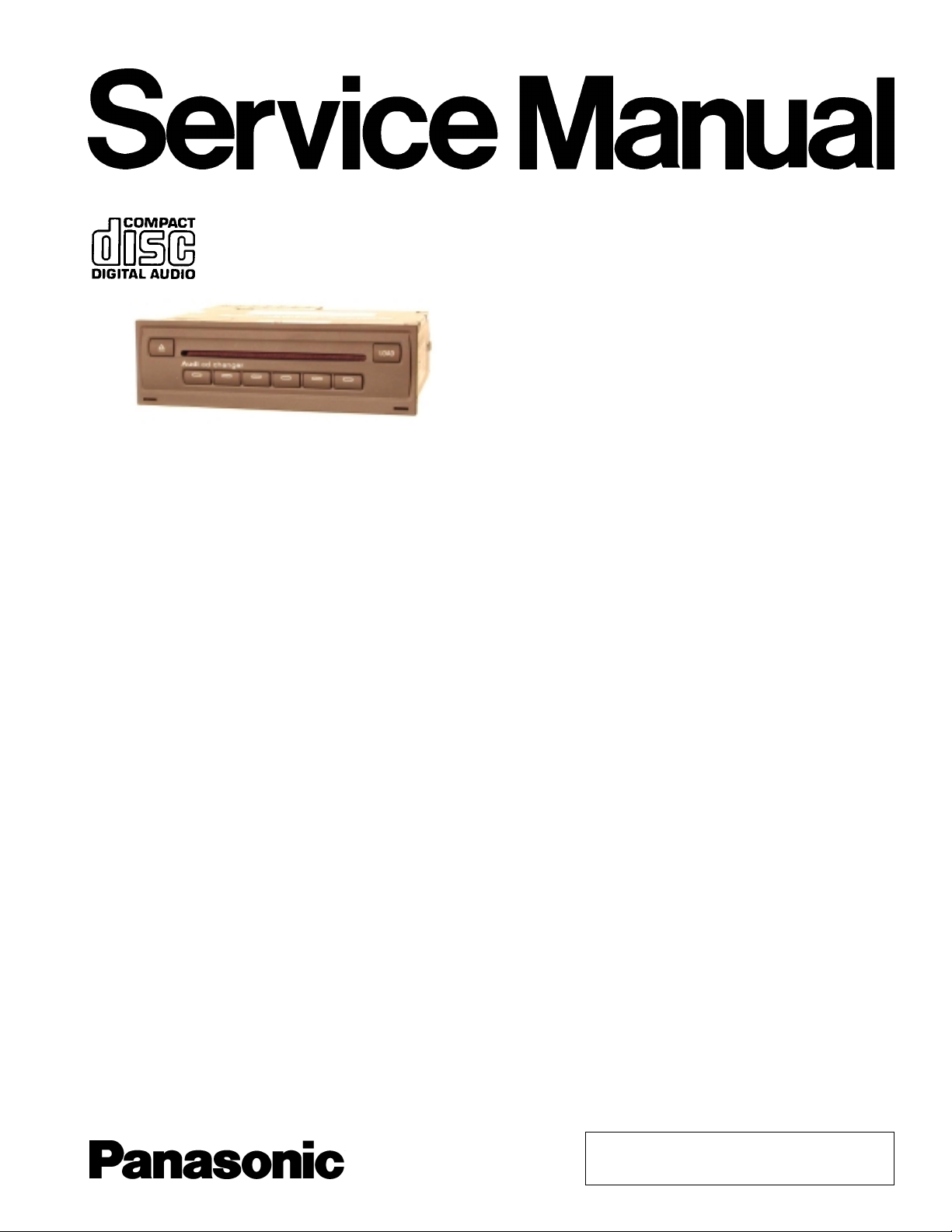
AUDI
CX-CA1270L
6-Disc CD Changer
PART No. : 4E0 035 111
VEHICLE : Audi A8
DESTINATION : All Countries
PRODUCED AFTER : Jan., 2002
General
Power Supply DC 12V (11V - 16V),
Test Voltage 13.2V
Negative Ground
Current Consumption Less than 3.0A (at 0.5W)
Power Output 30W×4
Output Impedance 4Ω
AM Radio
Frequency Range 530 - 1,710kHz
Usable Sensitivity 24dB/µV (S/N 20dB)
FM Stereo Radio
Frequency Range 87.75 - 107.9MHz
Usable Sensitivity 7dB/µV (S/N 30dB)
IDC
Signal to Noise Ratio More than 68dB (IHF-A)
Total Harmonic Distortion Less than 0.4%
Channel Separation 65dB (IHF-A)
Dimensions** (W×H×D) 209×86×164mm
Weight** 2.1kg
* Specifications and the design are subject to possible modification
without notice due to improvements.
** Dimensions and Weight shown are approximate.
© 2002 Matsushita Communication Industrial Co.,
Ltd. All rights reserved. Unauthorized copying and
distribution is a violation of law.
Page 2
AUDI / CX-CA1270L
CONTENTS
Page Page
1 FEATUERS 2
2 LASER PRODUCTS
3 FRONT VIEW
4 REAR AND TOP VIEW
5 WIRING CONNECTIONS
6 BLOCK DIAGRAM
7 TERMINALS DESCRIPTION
8 PACKAGE AND IC BLOCK DIAGRAM
9 REPLACEMENT PARTS LIST
10 EXPLODED VIEW (Unit) 14
11 CD CHANGER PARTS LIST
2
3
12 EXPLODED VIEW (CD Deck-1)
13 EXPLODED VIEW (CD Deck-2)
3
4
14 EXPLODED VIEW (CD Deck-3)
5
15 WIRING DIAGRAM
16 SCHEMATIC DIAGRAM-1
7
9
17 SCHEMATIC DIAGRAM-2
11
15
18
19
20
21
26
29
1 FEATUERS
•
• PLL (Phase Locked Loop) synthesized tuning.
• •
•
• 18-station preset (12-FM, 6-AM).
• •
•
• 6-Disc CD changer (in dash board).
• •
•
• Adjustable VOL, BAS, TRE, FAD and BAL.
• •
•
• GA-NET BUS.
• •
2 LASER PRODUCTS
2
Page 3
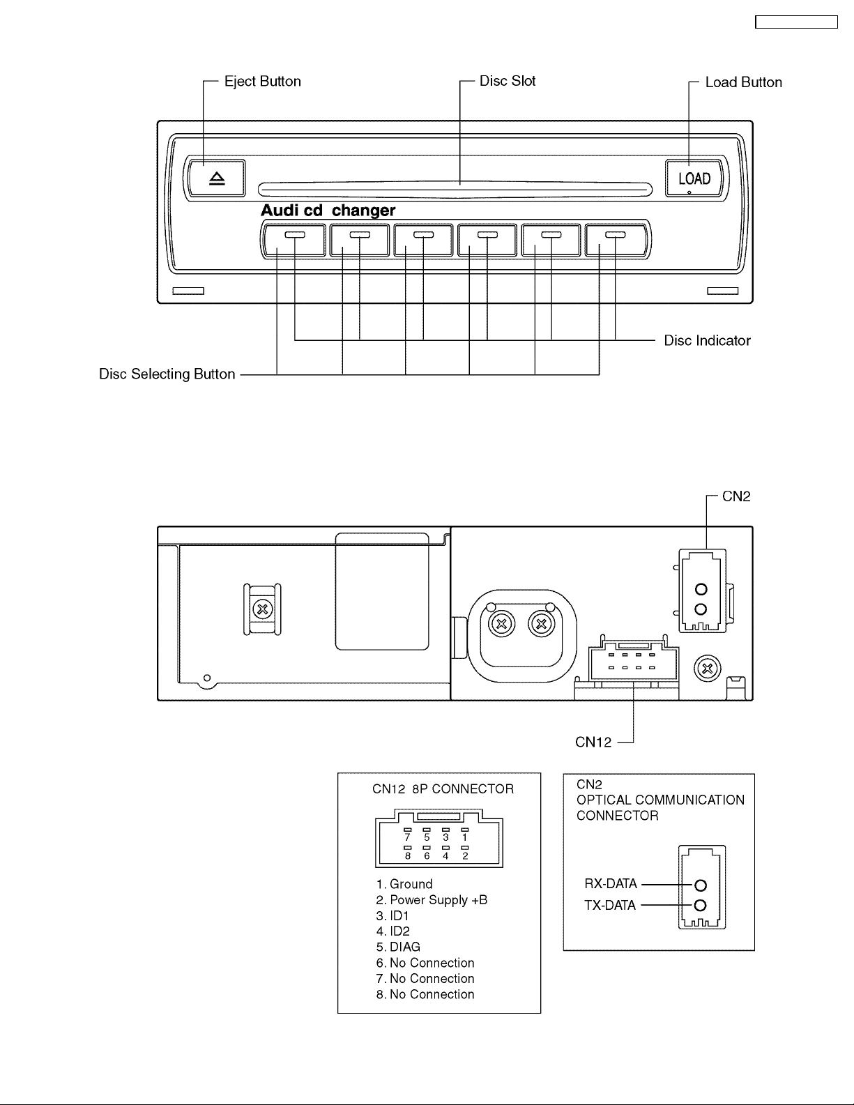
3 FRONT VIEW
AUDI / CX-CA1270L
4 REAR AND TOP VIEW
3
Page 4
AUDI / CX-CA1270L
5 WIRING CONNECTIONS
4
Page 5
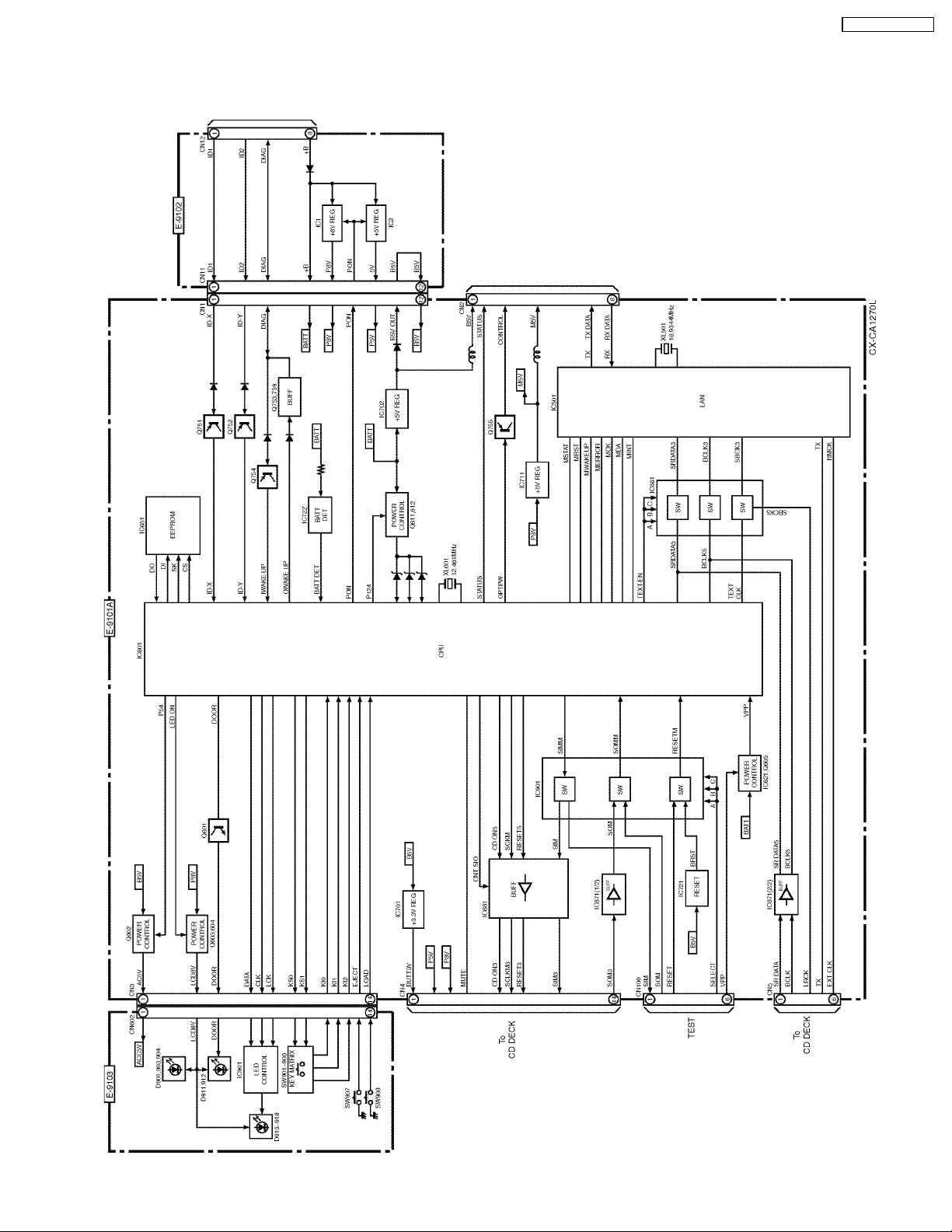
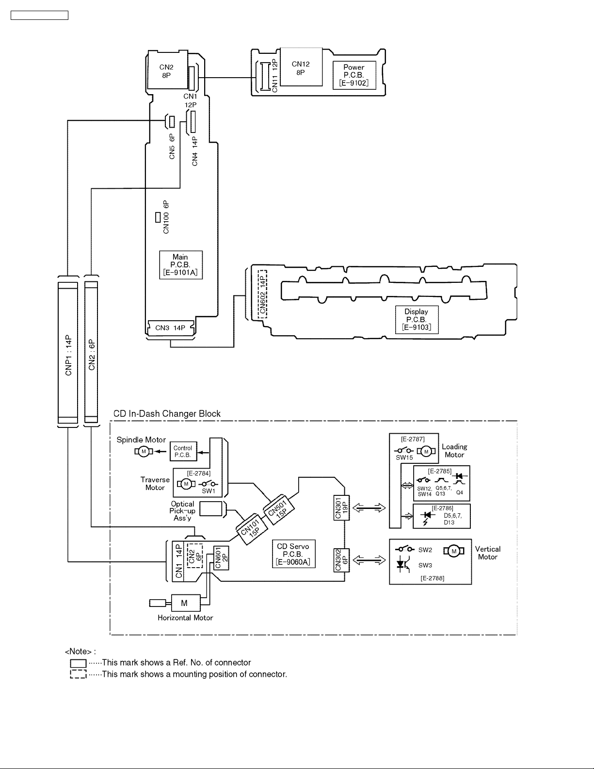
6 BLOCK DIAGRAM
6.1. Main/Power/Display Block
AUDI / CX-CA1270L
5
Page 6
AUDI / CX-CA1270L
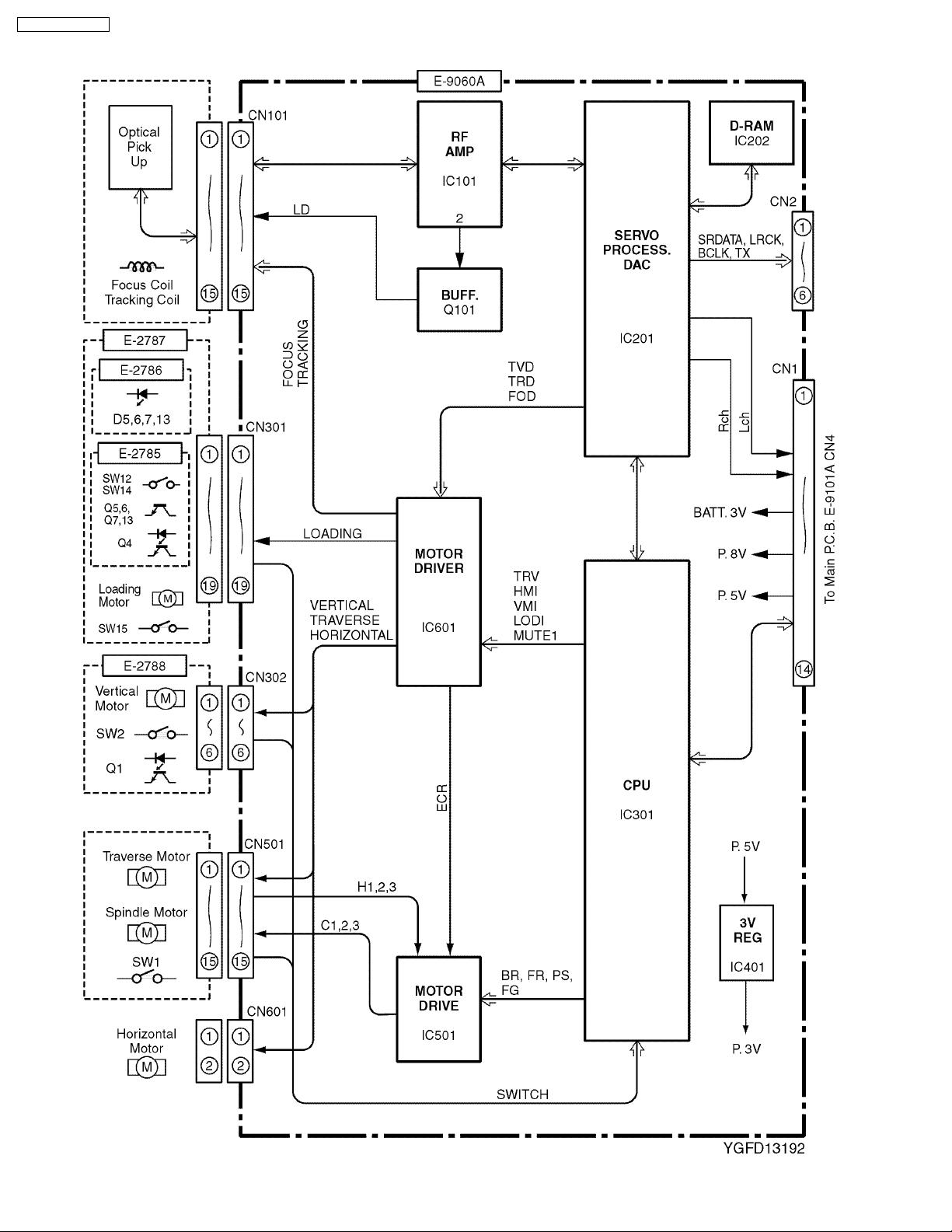
6.2. CD Servo Block
6
Page 7
7 TERMINALS DESCRIPTION
AUDI / CX-CA1270L
7.1. Main Block
IC601 : C2CBKH000010
Pin
No.
1 P120 Security ROM Select O 0
2 P121 Security data shift clock O 0
3 P122 Security data output O 0
4 P123 Security data input I 0
5 P124 Battery level detection control O 4.9
6-8 - No connection - -
9 VDD +5V digital power supply - 4.9
10 X2 Crystal ocillator - 3.1
11 X1 Crystal ocillator - 2.5
12 VSS Digital ground - 0
13 XT2 Not used - 14 XT1 (Connecting to Ground) - 0
15 RESET Reset I 4.9
16 M INT Interrupt input I 5.1
17 BATT-DET Battery level detection I 4.8
18 IWAKEUP Wake-up signal input I 0
19 EJECT Eject switch I 4.9
20 BCLK5 Shift clock for optical comm. LSI O 2.8
21 MAGA_IN Load switch I 4.9
22 STATUS Status signal O 0
23 AVDD +5V analog power supply - 4.8
24 AVREF +5V analog power supply - 4.8
25 7V_DET Battery level (7V) detection I 4.3
26 1V_DET Battery level (1V) detection I 1.0
27 GND Ground - 3.9
28-32GND (Connecting to Ground) - 0
Port Descriptions I/O Vol
(V)
Pin
No.
67 DOOR Door illumination on/off O 0
68 P54 ACC 5V power control O 4.8
69 PON System power control O 4.9
70 MON Not used - 71 MWAKEUP IC501 wake-up O 0
72 VSS Ground - 0
73 OWAKEUP wake-up signal output O 0
74-
76
77 MERROR IC501 error signal I 0
78 MSTAT IC501 status signal I 0
79,80NC No connection - -
81 VDD +5V digital power supply - 4.9
82 LED_ON LCD power control O 4.8
83-85NC No connection - -
86 MODE1 Not used - 87 MODE2 Not used - 88 DIAG1 Diag. signal input I 0
89 DIAG2 Diag. signal input I 0
90-92NC No connection - -
93 F_WRITE ROM data wirte control O 0
94 VPP ROM wite power supply - 0
95-
100
Port Descriptions I/O Vol
- No connection - -
NC No connection - -
(V)
33 AVSS Analog ground - 0
34 RX_RST Optical comm. Receiver reset O 0
35 NC No connection - 36 VDD +5V digital power supply - 4.8
37 SRDATA5 Serial data for optical comm. LSI O 0
38 NC No connection - 39 TEXTCLK Sub clock O 4.8
40 SOMM Serial data I 2.9
41 SIMM Serial data O 0
42 SCKM Shift clock O 4.8
43 CNT_SI0 Buffer gate on/off O 4.8
44 NC No connection - 45 MDA I/F data - 4.6
46 MRST Reset O 4.8
47 MCK I/F data shift clock O 5.0
48 MUTE Mute control O 0
49 TEXT_EN TEXT clock enable O 0
50 RX_ON Optical comm. Receiver power
control
51 NC No connection - -
52-55NC No connection - -
56 CDON5 CD power on O 4.9
57 RESET5 CD reset O 4.9
58 DATA LCD data O 0.5
59 CLK LCD data shift clock O 0.5
60 LCK LCD data load clock O 0
61 OPTPW Optical comm. controller power
on/off
62 KS1 Key strobe O 0
63 KS0 Key strobe O 0
64 KI2 Key data input I 0
64 KI1 Key data input I 0
66 KI0 Key data input I 4.9
O 0
O 0
7
Page 8
AUDI / CX-CA1270L
7.2. CD Servo Block
IC201 : MN662785TBUC
Pin
No.
1 DVDD3 +5V power supply - 3.6
2 D0 D-RAM data I/O 2.0
3 D1 D-RAM data I/O 2.0
4 NWE D-RAM data write O 3.0
5 NRAS D-RAM row address strobe O 3.2
6 D2 D-RAM data I/O 2.1
7 D3 D-RAM data I/O 1.9
8 NCAS0 D-RAM columun address strobe O 2.8
9 NCAS1 D-RAM columun address strobe O 1.4
10 A8 D-RAM address O 1.0
11-14 A7-4 D-RAM address O 1.1
15 A9 D-RAM address O 1.1
16-18 A0-A2 D-RAM address O 1.1
19 A3 D-RAM address O 1.1
20 DVSS2 Ground - 0
21 DVDD2 +5V power supply - 3.6
22 SPOUT Not used - 1.5
23 TRVP Traverse motor control O 1.9
24 TRVM Traverse motor control O 1.9
25 TRP Trackng coil drive O 1.9
26 TRM Trackng coil drive O 1.9
27 FDP Focus coil drive O 2.0
28 FDM Focus coil drive O 2.0
29 FBAL Focus balance O 1.9
30 TBAL Tracking balance O 1.9
31 CSEL (Connecting to VDD) - 3.6
32 FE Focus error I 2.0
33 TE Tracking error I 1.9
34 RFENV RF envelope I 1.9
35 OFT Off track signal I 0
36 NRFDET RF detecting signal I 0
37 BDO Drop-out signal I 0
38 LDON Laser on signal O 3.6
39 ARF RF signal I 1.9
40 IREF Reference current input I 1.2
41 ADPVCC (Connecting to ground) - 0
42 DSLF Loop filter for DSL - 2.0
43 DRF Loop filter for DSL - 2.2
44 PLLF Loop filter for PLL - 1.3
45 VCOF VCO filter - 1.3
46 AVDD2 +5V power supply - 3.6
47 AVSS2 Ground - 0
48 OUTL L channel output O 1.8
49 AVSS1 Ground - 0
50 OUTR R channel output O 1.8
51 AVDD1 +5V power supply - 3.5
52 FSEL (Connecting to P3V) - 3.7
53,54 - (Connecting to ground) - 0
55 FLAG Flag output O 0
56 CLVS Servo status signal O 3.6
57-60 - Not used - -
61 MCLK Clock for I/F command I 2.4
62 MDATA Date for I/F command I 1.9
63 MLD I/F command load I 3.5
64 BLKCK Subcode block clock O 0
65 SQCK Ext.clock for sub code-Q I 3.5
66 SUBQ Code for sub. code-Q O 1.1
67 DMUTE Mute input I 0
68 STAT Status signal O 1.1
69 NRST Reset input I 3.6
70 SPPOL Not used - 71 PMCK Clock output O 2.0
72 SMCK Clock output O 1.9
73 SDATA Serial data O 0
74 LRCK LR clock O 0
75 BCLK Bit clock O 0
76 /TEST (Connecting to VDD) - 1.5
77 X1 Crystal oscillator - 1.8
78 X2 Crystal oscillator - 1.8
Port Descriptions I/O Vol
(V)
Pin
No.
79 DVDD1 +5V power supply - 3.6
80 DVSS1 Ground - 0
Port Descriptions I/O Vol
IC301 : C2BBGF000364
Pin
No.
1 PS Motor power save O 3.5
2 BR Brake mode selection O 0
3 GCTL Motor G-control O 1.6
4 SPCCTL Motor speed control O 3.5
5 - Not used - 6 MCLK Clock for I/F command O 2.9
7 MDATA Data for I/F command O 1.9
8 MLD I/F command losd O 3.5
9 VSS0 Ground - 0
10 VDD0 +3V power supply - 3.5
11 STAT Status signal I 1.2
12 FLOCK Focus servo lock O 0
13 TLOCK Tracking servo lock O 0
14 SENS Servo status O 0
15 SIM CD changerserial data I 3.1
16 SOM CD changerserial data O 2.2
17 SCKM Serial data shift clock I 3.2
18 SUBQ Code for sub. code-Q I 1.7
19 - Not used - 20 SQCK Ext. clock for sub. code-Q O 3.6
21 NRST Reset output O 3.6
22 DMUTE Mute output O 0
23 MUTE Mute output O 0
24 VDD1 +3V power supply - 3.5
25 AVSS1 Ground - 0
26 SW15 Feeder SW I 3.6
27 SW3 Tray H SW I 3.5
28 SW4 Disc push SW I 0.5
29 SW5 Disc SW I 0
30 SW6 Disc load SW I 0
31 SW7 Eject SW I 0
32 SW13 Eject2 SW I 0
33 CLVS Servo status O 3.6
34 AVREF +3V power supply - 3.6
35 - Not used - 36 /RESET Reset I 3.6
37 XT2 Not used - 38 XT1 (VDD pull-up) - 3.6
39 IC(VPP) (Connecting to ground) - 0
40 X2 Crystal Osillator - 2.1
41 X1 Crystal Osillator - 1.8
42 VSS1 Ground - 0
43 CDON CD changer start/stop I 3.1
44 BLKCK Sub. code block clock I 0
45 FG Flag signal I 1.9
46 BD0 Drop-out signal I 0
47 FR Revolution detection I 0
48 TRV Forced traverse control O 1.9
49 PWM Not used - 50 VMI+ Horizontal motor control O 0
51 VMI- Horizontal motor control O 0
52 MUTE1 Mute output O 3.6
53 LODI+ Loading motor control O 0
54 LODI- Loading motor control O 0
55 HMI+ Vertical motor control O 0
56 HMI- Vertical motor control O 0
57 SW1 Inner SW I 3.6
58 SW2 TrayG SW I 0
59 SW8 Play SW I 0
60 SW9 Clump SW I 3.6
61 SW10 Shuter SW I 3.6
62 SW11 Horizontal origin SW I 3.6
63 SW12 Outer2 SW I 3.7
64 SW14 Outer SW I 3.6
Port Descriptions I/O Vol
(V)
(V)
8
Page 9
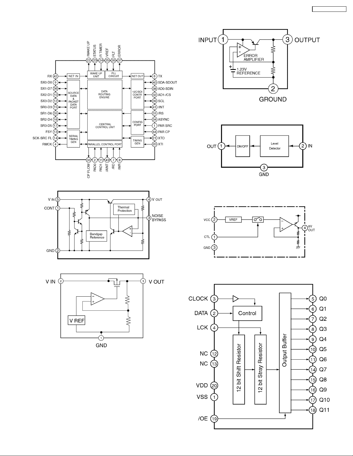
8 PACKAGE AND IC BLOCK DIAGRAM
8.1. Main Block
AUDI / CX-CA1270L
IC702 : LP2950CDT
IC501 : C1EB00000047
IC621 : C0CBAJC00006
IC721 : MN1382QPIC
8.2. Power Block
IC1 : C0DAZHG00001
8.3. Display Block
IC701 : C0CBABC00039
IC901 : C0GBA0000002
9
Page 10

AUDI / CX-CA1270L
8.4. CD Servo Block
IC202 : C3ABMB000009
IC501 : C0GBH0000006
IC601 : C0GBY0000014
10
Page 11

9 REPLACEMENT PARTS
LIST
Notes :
1. Be sure to make your orders of replacement parts
according to this list.
2. Important safety notice: Components, identified by
have special characteristics important for safety. When
replacing any of these components, use only
manufacturer´s specified parts.
3. Location keys in the remarks column indicates the general
location of the parts shown in the exploded drawing, as in a
road map.
4. The marking (RTL) indicates that Retention Time is limited
for this item. After the discontinuation of assembly in
production, the item will continue to be available for a
specific period of time. The retention period of availability is
dependent on the type of assembly, and in accordance with
the laws governing part and product retention. After the end
of this period, the assembly will no longer be available.
5. "MCD" marks in remarks column are indicated supply parts
of Matsushita Communication Deutschland GmbH (MCD).
Ref.
No.
[E-9101A] Main Block
IC´s AND TRANSISTORs
IC501 C1EB00000047 IC
IC601 C2CBKH000010 IC
IC621 C0CBAJC00006 IC
IC651 C3EBEG000025 IC
IC661 C0JBAZ000903 IC
IC671 C0JBAZ001229 IC
IC681 C0JBAZ001754 IC
IC701 C0CBABC00039 IC
IC702 C0CVADC00035 IC
IC711 C0CBADG00005 IC
IC721 MN1382QP IC
IC722 C0EBM0000009 IC
IC901 C0JBAZ000903 IC
Q601 B1GBCFJN0009 Transistor
Q602 B1GDCFNN0002 Transistor
Q603 B1GBCFJN0009 Transistor
Q604 2SB0766AWL Transistor
Q605 2SB0766AWL Transistor
Q611 B1GBCFJN0009 Transistor
Q612 B1GDCFNN0007 Transistor
Q751 B1ABCF000042 Transistor
Q752 B1ABCF000042 Transistor
Q753 B1ABCF000044 Transistor
Q754 B1ABCF000042 Transistor
Q755 B1GDCFGG0002 Transistor
Q759 B1ABCF000044 Transistor
Q780 B1GDCFJN0011 Transistor
Q781 B1GBCFNN0009 Transistor
Diodes
D601 B0ECKP000002 Diode
D611 MA8033-HTX Diode
D612 MA8043MTX Diode
D613 MA8051-HTX Diode
D614 MA8043MTX Diode
D615 MA8091-HTX Diode
D616 MA8043MTX Diode
D630 MAZ805600L Diode
D631 MAZ805600L Diode
D632 MAZ805600L Diode
Part No. Part Name & Description Remarks
mark
Ref.
No.
D633 MAZ805600L Diode
D634 MAZ805600L Diode
D635 MAZ805600L Diode
D636 MAZ805600L Diode
D637 MAZ805600L Diode
D638 MAZ805600L Diode
D639 MAZ805600L Diode
D701 B0ECKP000004 Diode
D751 MA3X152A0L Diode
D752 MA3X152A0L Diode
D753 MA3X152A0L Diode
D755 MA8091-HTX Diode
D756 MA3X152A0L Diode
CAPACITORs
C501 F1H1C104A005 Ceramic, 0.1µF 16WV
C502 F1H1C104A005 Ceramic, 0.1µF 16WV
C503 F1H1C104A005 Ceramic, 0.1µF 16WV
C504 F1H1C104A005 Ceramic, 0.1µF 16WV
C505 F1H1C104A005 Ceramic, 0.1µF 16WV
C507 F1H1C104A005 Ceramic, 0.1µF 16WV
C508 F3G1C106A001 Ceramic, 10µF 16WV
C601 F1H1H150A231 Ceramic, 15PF 50WV
C602 F1H1H150A231 Ceramic, 15PF 50WV
C603 F1H1C104A005 Ceramic, 0.1µF 16WV
C604 F1H1E223A011 Ceramic, 0.022µF 25WV
C605 F1H1H103A201 Ceramic, 0.01µF 25WV
C606 F1H1C104A005 Ceramic, 0.1µF 16WV
C608 F1J1C1050013 Ceramic, 1µF 16WV
C609 F1H1C104A005 Ceramic, 0.1µF 16WV
C651 F1H1C104A005 Ceramic, 0.1µF 16WV
C661 F1H1C104A005 Ceramic, 0.1µF 16WV
C671 F1H1C104A005 Ceramic, 0.1µF 16WV
C681 F1H1C104A005 Ceramic, 0.1µF 16WV
C701 F1H1C104A005 Ceramic, 0.1µF 16WV
C702 ECEV0JA470SR Electrolytic, 47µF 6.3WV
C703 ECEV1CA220SR Electrolytic, 22µF 16WV
C704 F1H1C104A005 Ceramic, 0.1µF 16WV
C705 F1H1C104A005 Ceramic, 0.1µF 16WV
C706 F3G1C106A001 Ceramic, 10µF 16WV
C711 F1H1C104A005 Ceramic, 0.1µF 16WV
C712 ECEV0JA470SR Electrolytic, 47µF 6.3WV
C713 F1H1C104A005 Ceramic, 0.1µF 16WV
C721 F1H1C104A005 Ceramic, 0.1µF 16WV
C722 ECEV0JA470SR Electrolytic, 47µF 6.3WV
C723 F1H1C104A005 Ceramic, 0.1µF 16WV
C751 F1H1C473A005 Ceramic, 0.047µF 16WV
C752 F3G1C106A001 Ceramic, 10µF 16WV
C753 F1H1C104A005 Ceramic, 0.1µF 16WV
C754 F3G1C106A001 Ceramic, 10µF 16WV
C755 F1H1C104A005 Ceramic, 0.1µF 16WV
C756 ECEV1AA470P Electrolytic, 47µF 10WV
C757 F1H1C104A005 Ceramic, 0.1µF 16WV
C758 F1H1C104A005 Ceramic, 0.1µF 16WV
RESISTORs
L504 ERJ6GEY0R00V Chip, 0ΩΩΩΩ 1/10W
L753 ERJ6GEY0R00V Chip, 0ΩΩΩΩ 1/10W
R501 ERJ3GEYJ151V Chip, 150ΩΩΩΩ 1/16W
R502 ERJ3GEYJ470V Chip, 47ΩΩΩΩ 1/16W
R503 ERJ3GEYJ473V Chip, 47kΩΩΩΩ 1/16W
R505 ERJ3GEYJ394V Chip, 390kΩΩΩΩ 1/16W
R507 ERJ3GEYJ222V Chip, 2.2kΩΩΩΩ 1/16W
R508 ERJ3GEYJ103V Chip, 10kΩΩΩΩ 1/16W
R509 ERJ3GEYJ472V Chip, 4.7kΩΩΩΩ 1/16W
R510 ERJ3GEYJ472V Chip, 4.7kΩΩΩΩ 1/16W
R511 ERJ3GEYJ472V Chip, 4.7kΩΩΩΩ 1/16W
R602 ERJ3GEYJ472V Chip, 4.7kΩΩΩΩ 1/16W
R603 ERJ3GEYJ472V Chip, 4.7kΩΩΩΩ 1/16W
R606 ERJ3GEYJ103V Chip, 10kΩΩΩΩ 1/16W
R608 ERJ3GEYJ473V Chip, 47kΩΩΩΩ 1/16W
Part No. Part Name & Description Remarks
AUDI / CX-CA1270L
11
Page 12

AUDI / CX-CA1270L
Ref.
No.
R609 ERJ3GEYJ473V Chip, 47kΩΩΩΩ 1/16W
R610 ERJ3GEY0R00V Chip, 0ΩΩΩΩ 1/16W
R611 ERJ3GEYJ471V Chip, 470ΩΩΩΩ 1/16W
R612 ERJ3GEYJ122V Chip, 1.2kΩΩΩΩ 1/16W
R613 ERJ3GEYJ471V Chip, 470ΩΩΩΩ 1/16W
R614 ERJ3GEYJ102V Chip, 1kΩΩΩΩ 1/16W
R615 ERJ3GEYJ471V Chip, 470ΩΩΩΩ 1/16W
R616 ERJ3GEYJ271V Chip, 270ΩΩΩΩ 1/16W
R617 ERJ3GEYJ103V Chip, 10kΩΩΩΩ 1/16W
R618 ERJ3GEYJ103V Chip, 10kΩΩΩΩ 1/16W
R619 ERJ3GEYJ103V Chip, 10kΩΩΩΩ 1/16W
R620 ERJ3GEYJ222V Chip, 2.2kΩΩΩΩ 1/16W
R630 ERJ3GEYJ102V Chip, 1kΩΩΩΩ 1/16W
R631 ERJ3GEYJ102V Chip, 1kΩΩΩΩ 1/16W
R632 ERJ3GEYJ102V Chip, 1kΩΩΩΩ 1/16W
R633 ERJ3GEYJ102V Chip, 1kΩΩΩΩ 1/16W
R634 ERJ3GEYJ102V Chip, 1kΩΩΩΩ 1/16W
R635 ERJ3GEYJ102V Chip, 1kΩΩΩΩ 1/16W
R636 ERJ3GEYJ102V Chip, 1kΩΩΩΩ 1/16W
R637 ERJ3GEYJ102V Chip, 1kΩΩΩΩ 1/16W
R638 ERJ3GEYJ102V Chip, 1kΩΩΩΩ 1/16W
R639 ERJ3GEYJ102V Chip, 1kΩΩΩΩ 1/16W
R651 ERJ3GEYJ103V Chip, 10kΩΩΩΩ 1/16W
R652 ERJ3GEYJ103V Chip, 10kΩΩΩΩ 1/16W
R653 ERJ3GEYJ103V Chip, 10kΩΩΩΩ 1/16W
R661 ERJ3GEYJ104V Chip, 100kΩΩΩΩ 1/16W
R671 ERJ3GEYJ473V Chip, 47kΩΩΩΩ 1/16W
R672 ERJ3GEYJ473V Chip, 47kΩΩΩΩ 1/16W
R673 ERJ3GEYJ332V Chip, 3.3kΩΩΩΩ 1/16W
R674 ERJ3GEYJ474V Chip, 470kΩΩΩΩ 1/16W
R675 ERJ3GEYJ182V Chip, 1.8kΩΩΩΩ 1/16W
R676 ERJ3GEY0R00V Chip, 0ΩΩΩΩ 1/16W
R677 ERJ3GEY0R00V Chip, 0ΩΩΩΩ 1/16W
R681 ERJ3GEYJ104V Chip, 100kΩΩΩΩ 1/16W
R683 ERJ3GEY0R00V Chip, 0ΩΩΩΩ 1/16W
R751 ERJ3GEYJ472V Chip, 4.7kΩΩΩΩ 1/16W
R752 ERJ3GEYJ473V Chip, 47kΩΩΩΩ 1/16W
R753 ERJ3GEYJ103V Chip, 10kΩΩΩΩ 1/16W
R754 ERJ3GEYJ472V Chip, 4.7kΩΩΩΩ 1/16W
R755 ERJ3GEYJ473V Chip, 47kΩΩΩΩ 1/16W
R756 ERJ3GEYJ103V Chip, 10kΩΩΩΩ 1/16W
R757 ERJ3GEYJ473V Chip, 47kΩΩΩΩ 1/16W
R758 ERJ3GEYJ332V Chip, 3.3kΩΩΩΩ 1/16W
R759 ERJ3GEYJ153V Chip, 15kΩΩΩΩ 1/16W
R760 ERJ3GEYJ101V Chip, 100ΩΩΩΩ 1/16W
R761 ERJ3GEYJ223V Chip, 22kΩΩΩΩ 1/16W
R762 ERJ3GEYJ104V Chip, 100kΩΩΩΩ 1/16W
R763 ERJ3GEYJ472V Chip, 4.7kΩΩΩΩ 1/16W
R764 ERJ3GEYJ470V Chip, 47ΩΩΩΩ 1/16W
R767 ERJ3GEYJ333V Chip, 33kΩΩΩΩ 1/16W
R768 ERJ3GEYJ333V Chip, 33kΩΩΩΩ 1/16W
R769 ERJ3GEYJ100V Chip, 10ΩΩΩΩ 1/16W
R770 ERJ3GEYJ104V Chip, 100kΩΩΩΩ 1/16W
R771 ERJ3GEYJ104V Chip, 100kΩΩΩΩ 1/16W
R780 ERJ3GEYJ101V Chip, 100ΩΩΩΩ 1/16W
R910 ERJ3GEYJ473V Chip, 47kΩΩΩΩ 1/16W
Part No. Part Name & Description Remarks
Ref.
No.
CRYSTALs
XL501 H2D169500008 Crystal
XL601 H0J124500002 Crystal
[E-9102] Power Block
IC´s AND TRANSISTORs
IC1 C0DAZHG00001 IC
IC2 C0CAZDG00001 IC
Diodes
D1 B0BA04700004 Diode
D2 B0BA04700001 Diode
CAPACITORs
C1 ECA1CM102B Electrolytic, 1000µF 16WV
C2 ECA1AM471B Electrolytic, 470µF 10WV
C3 ECA0JM471B Electrolytic, 470µF 6.3WV
C5 F4D552230004 Electrolytic, 0.022F 5.5WV
CONNECTORs
CN11 K1KB12A00004 Connector, 12P
CN12 K1FA108B0013 Connector, 8P
[E-9103] Display Block
IC´s AND TRANSISTORs
IC901 C0GBA0000002 IC
DIODEs
D901 B3AAB0000130 Diode
D903 B3AAB0000130 Diode
D904 B3AAB0000130 Diode
D911 B3AAB0000130 Diode
D912 B3AAB0000130 Diode
D913 B3AAB0000130 Diode
D914 B3AAB0000130 Diode
D915 B3AAB0000130 Diode
D916 B3AAB0000130 Diode
D917 B3AAB0000130 Diode
D918 B3AAB0000130 Diode
D920 B3AAB0000130 Diode
D921 B3AAB0000130 Diode
CAPACITOR
C902 F1J1C104A005 Ceramic, 0.1µF 16WV
Part No. Part Name & Description Remarks
CONNECTORs
CN1 K1KA12B00007 Connector, 12P
CN100 K1MN06B00008 Connector, 6P
CN2 K7ACAA000002 Connector, 8P
CN3 K1KB14B00015 Connector, 14P
CN4 K1MN14B00020 Connector, 14P
CN5 K1MN06B00008 Connector, 6P
COILs
L102 F1Z1E2220001 Coil
L501 J0JCC0000053 Coil
L503 J0JCC0000053 Coil
L751 F1Z1E2220001 Coil
L752 F1Z1E2220001 Coil
RESISTORs
J901 ERJ8GEY0R00V Chip, 0ΩΩΩΩ 1/8W
J902 ERJ8GEY0R00V Chip, 0ΩΩΩΩ 1/8W
J903 ERJ8GEY0R00V Chip, 0ΩΩΩΩ 1/8W
J904 ERJ8GEY0R00V Chip, 0ΩΩΩΩ 1/8W
J905 ERJ8GEY0R00V Chip, 0ΩΩΩΩ 1/8W
J906 ERJ8GEY0R00V Chip, 0ΩΩΩΩ 1/8W
J907 ERJ8GEY0R00V Chip, 0ΩΩΩΩ 1/8W
J908 ERJ8GEY0R00V Chip, 0ΩΩΩΩ 1/8W
J909 ERJ8GEY0R00V Chip, 0ΩΩΩΩ 1/8W
J910 ERJ8GEY0R00V Chip, 0ΩΩΩΩ 1/8W
J911 ERJ8GEY0R00V Chip, 0ΩΩΩΩ 1/8W
R904 ERJ8GEYJ392V Chip, 3.9kΩΩΩΩ 1/8W
R905 ERJ6GEYJ392 Chip, 3.9kΩΩΩΩ 1/10W
R906 ERJ8GEYJ152V Chip, 1.5kΩΩΩΩ 1/8W
R907 ERJ8GEYJ152V Chip, 1.5kΩΩΩΩ 1/8W
12
Page 13

Ref.
No.
R908 ERJ8GEYJ152V Chip, 1.5kΩΩΩΩ 1/8W
R909 ERJ8GEYJ152V Chip, 1.5kΩΩΩΩ 1/8W
R910 ERJ8GEYJ152V Chip, 1.5kΩΩΩΩ 1/8W
R911 ERJ8GEYJ152V Chip, 1.5kΩΩΩΩ 1/8W
R912 ERJ6GEYJ152 Chip, 1.5kΩΩΩΩ 1/10W
R913 ERJ6GEYJ152 Chip, 1.5kΩΩΩΩ 1/10W
CONNECTOR
CN602 K1KA14A00154 Connector, 14P
SWITCHEs
SW901 YEAS09320 Switch
SW902 YEAS09320 Switch
SW903 YEAS09320 Switch
SW904 YEAS09320 Switch
SW905 YEAS09320 Switch
SW906 YEAS09320 Switch
SW907 YEAS09320 Switch
SW908 YEAS09320 Switch
Mechanical Parts
MISCELLANEOUS
AT1 K4CD01000002 Bracket, GND
AT2 K4CD01000002 Bracket, GND
1 YEP0PT9101Z9 PCB w/Component RTL
2 FEFX0214539B Bracket, PCB Fixed
3 YEFM031271 Laser Seal
5 YEFA031799 Upper Cover
6 YEFA08559 Rear Chassis
8 YEFX9992667 Disc Guide
9 YEFS011826 Dust Felt
10 YEP0PT9103Z9 PCB w/Component RTL
11 YEFC027378 Escutchon Ass´y
13 YEFA05820 Connector Cover
14 YEFX0215803 Bracket, Reg.
15 YEP0PT9102Z9 PCB w/Component RTL
16 YEFA011968 Chassis Ass´y
Part No. Part Name & Description Remarks
AUDI / CX-CA1270L
21 YEJT03009 Screw, M3x8mm
22 YEJT03142 Screw,
23 XTB3+5FFX Screw, M3x5mm
24 XTB2+6GFX Screw, M2x6mm
25 XQN2+B5FZ Screw, M2x5mm
13
Page 14

AUDI / CX-CA1270L
10 EXPLODED VIEW (Unit)
14
Page 15

11 CD CHANGER PARTS
LIST
Ref.
No.
[E9060A] CD Servo Block
IC´s and TRANSISTORs
IC101 C1BB00000624 IC
IC201 MN662785TBUC IC
IC202 C3ABMB000009 IC
IC301 C2BBGF000364 IC
IC401 C0DBZGE00002 IC
IC501 C0GBH0000006 IC
IC601 C0GBY0000014 IC
Q101 2SB766ATX Transistor
DIODE
D301 MA152WKTX Diode
CAPACITORs
C1 EEVFC0J102P Electrolytic, 1000µF 6.3WV
C101 F1H1C104A005 Ceramic, 0.1µF 16WV
C102 F1H1C104A005 Ceramic, 0.1µF 16WV
C103 F3H0J1070005 Tantalum, 100µF 6.3WV
C104 F1H1C104A005 Ceramic, 0.1µF 16WV
C105 F1H1C104A005 Ceramic, 0.1µF 16WV
C106 F1H1H8210002 Ceramic, 820PF 50WV
C107 F1H1C104A005 Ceramic, 0.1µF 16WV
C108 F1H1H682A190 Ceramic, 6800PF 50WV
C109 F1H1H222A190 Ceramic, 2200PF 50WV
C110 F1K0J1060015 Ceramic, 10 µF 6.3WV
C111 F1H1H1010005 Ceramic, 100PF 50WV
C112 F1H1E103A011 Ceramic, 0.01µF 25WV
C113 F1H1E103A011 Ceramic, 0.01µF 25WV
C114 F1H1H2710006 Ceramic, 270PF 50WV
C115 F1H1H6810005 Ceramic, 680PF 50WV
C116 F1H1C104A005 Ceramic, 0.1µF 16WV
C117 F1K0J1060015 Ceramic, 10 µF 6.3WV
C201 F1H1C104A005 Ceramic, 0.1µF 16WV
C202 F1H1E123A011 Ceramic, 0.012µF 25WV
C203 YECUZ1A224KX Ceramic, 0.22µF 10WV
C205 F1H1A4740004 Ceramic, 0.47µF 10WV
C206 F1K0J1060015 Ceramic, 10 µF 6.3WV
C208 EEVFC0J102P Electrolytic, 1000µF 6.3WV
C209 F1K0J1060015 Ceramic, 10 µF 6.3WV
C210 F1H0J1050010 Ceramic, 1µF 6.3WV
C211 F1H0J1050010 Ceramic, 1µF 6.3WV
C301 F1K0J1060015 Ceramic, 10 µF 6.3WV
C302 F1H1E103A011 Ceramic, 0.01µF 25WV
C312 F1H1C104A005 Ceramic, 0.1µF 16WV
C313 F1H1C104A005 Ceramic, 0.1µF 16WV
C315 F1H1C104A005 Ceramic, 0.1µF 16WV
C401 F1H0J1050010 Ceramic, 1µF 6.3WV
C402 F1K0J1060015 Ceramic, 10 µF 6.3WV
C501 F1H1C104A005 Ceramic, 0.1µF 16WV
C502 F1H1C104A005 Ceramic, 0.1µF 16WV
C503 F1H1C104A005 Ceramic, 0.1µF 16WV
C504 YECUZ1C104KX Ceramic, 0.1µF 16WV
C601 F1H1H8210002 Ceramic, 820PF 50WV
C602 F1H1H8210002 Ceramic, 820PF 50WV
C603 F1H0J1050010 Ceramic, 1µF 6.3WV
C604 YECUZ1C333KX Ceramic, 0.033µF 16WV
C605 F1H1C104A005 Ceramic, 0.1µF 16WV
C606 F1H1C104A005 Ceramic, 0.1µF 16WV
C607 ECEV1CA470SP Electrolytic, 47µF 16WV
C608 F1K0J1060015 Ceramic, 10 µF 6.3WV
RESISTORs
R1 ERJ3GEYJ334V Chip, 330kΩΩΩΩ 1/16W
R2 ERJ3GEYJ102V Chip, 1kΩΩΩΩ 1/16W
Part No. Part Name & Description Remarks
Ref.
No.
R3 ERJ3GEYJ102V Chip, 1kΩΩΩΩ 1/16W
R101 ERJ6GEYJ1R0V Chip, 1.0ΩΩΩΩ 1/10W
R102 ERJ3GEY0R00V Chip, 0ΩΩΩΩ 1/16W
R103 ERJ3GEY0R00V Chip, 0ΩΩΩΩ 1/16W
R104 ERJ3GEYJ152V Chip, 1.5kΩΩΩΩ 1/16W
R105 ERJ3GEYJ152V Chip, 1.5kΩΩΩΩ 1/16W
R106 ERJ3GEYJ563V Chip, 56kΩΩΩΩ 1/16W
R107 ERJ3GEYJ223V Chip, 22kΩΩΩΩ 1/16W
R108 ERJ3GEYJ333V Chip, 33kΩΩΩΩ 1/16W
R109 ERJ3GEYJ473V Chip, 47kΩΩΩΩ 1/16W
R110 ERJ3GEYJ102V Chip, 1kΩΩΩΩ 1/16W
R111 ERJ3GEYJ102V Chip, 1kΩΩΩΩ 1/16W
R201 ERJ3GEYJ823V Chip, 82kΩΩΩΩ 1/16W
R202 ERJ3GEYJ473V Chip, 47kΩΩΩΩ 1/16W
R203 ERJ3GEYJ473V Chip, 47kΩΩΩΩ 1/16W
R204 ERJ3GEYJ271V Chip, 270ΩΩΩΩ 1/16W
R205 ERJ3GEYJ222V Chip, 2.2kΩΩΩΩ 1/16W
R206 ERJ3GEYJ330V Chip, 33ΩΩΩΩ 1/16W
R207 ERJ3GEYJ102V Chip, 1kΩΩΩΩ 1/16W
R208 ERJ3GEYJ102V Chip, 1kΩΩΩΩ 1/16W
R209 ERJ3GEYJ102V Chip, 1kΩΩΩΩ 1/16W
R210 ERJ3GEYJ102V Chip, 1kΩΩΩΩ 1/16W
R211 ERJ3GEYJ332V Chip, 3.3kΩΩΩΩ 1/16W
R212 ERJ3GEYJ332V Chip, 3.3kΩΩΩΩ 1/16W
R213 ERJ3GEYJ105V Chip, 1MΩΩΩΩ 1/16W
R214 ERJ3GEYJ151V Chip, 150ΩΩΩΩ 1/16W
R301 ERJ3GEYJ563V Chip, 56kΩΩΩΩ 1/16W
R302 ERJ3GEYJ563V Chip, 56kΩΩΩΩ 1/16W
R303 ERJ3GEYJ332V Chip, 3.3kΩΩΩΩ 1/16W
R304 ERJ3GEYJ332V Chip, 3.3kΩΩΩΩ 1/16W
R305 ERJ3GEYJ563V Chip, 56kΩΩΩΩ 1/16W
R306 ERJ3GEYJ563V Chip, 56kΩΩΩΩ 1/16W
R307 ERJ3GEYJ683V Chip, 68kΩΩΩΩ 1/16W
R308 ERJ3GEYJ683V Chip, 68kΩΩΩΩ 1/16W
R309 ERJ3GEYJ683V Chip, 68kΩΩΩΩ 1/16W
R310 ERJ3GEYJ332V Chip, 3.3kΩΩΩΩ 1/16W
R311 ERJ3GEYJ332V Chip, 3.3kΩΩΩΩ 1/16W
R312 ERJ3GEYJ332V Chip, 3.3kΩΩΩΩ 1/16W
R313 ERJ3GEYJ332V Chip, 3.3kΩΩΩΩ 1/16W
R314 ERJ3GEYJ332V Chip, 3.3kΩΩΩΩ 1/16W
R315 ERJ3GEYJ683V Chip, 68kΩΩΩΩ 1/16W
R316 ERJ3GEYJ332V Chip, 3.3kΩΩΩΩ 1/16W
R317 ERJ3GEYJ221V Chip, 220ΩΩΩΩ 1/16W
R318 ERJ3GEYJ221V Chip, 220ΩΩΩΩ 1/16W
R319 ERJ3GEYJ221V Chip, 220ΩΩΩΩ 1/16W
R320 ERJ3GEYJ221V Chip, 220ΩΩΩΩ 1/16W
R321 ERJ3GEYJ221V Chip, 220ΩΩΩΩ 1/16W
R322 ERJ3GEYJ221V Chip, 220ΩΩΩΩ 1/16W
R323 ERJ3GEYJ103V Chip, 10kΩΩΩΩ 1/16W
R324 ERJ3GEYJ103V Chip, 10kΩΩΩΩ 1/16W
R325 ERJ3GEYJ332V Chip, 3.3kΩΩΩΩ 1/16W
R326 ERJ3GEYJ473V Chip, 47kΩΩΩΩ 1/16W
R327 ERJ3GEY0R00V Chip, 0ΩΩΩΩ 1/16W
R330 ERJ3GEYJ332V Chip, 3.3kΩΩΩΩ 1/16W
R501 ERJ3GEYJ121V Chip, 120ΩΩΩΩ 1/16W
R502 ERJ8GEYJ1R0V Chip, 1.0ΩΩΩΩ 1/8W
R503 ERJ3GEYJ121V Chip, 120ΩΩΩΩ 1/16W
R504 ERJ3GEYJ183V Chip, 18kΩΩΩΩ 1/16W
R505 ERJ3GEYJ563V Chip, 56kΩΩΩΩ 1/16W
R601 ERJ3GEYJ103V Chip, 10kΩΩΩΩ 1/16W
R602 ERJ3GEYJ153V Chip, 15kΩΩΩΩ 1/16W
R603 ERJ3GEYJ103V Chip, 10kΩΩΩΩ 1/16W
R604 ERJ3GEYJ153V Chip, 15kΩΩΩΩ 1/16W
R605 ERJ3GEYJ332V Chip, 3.3kΩΩΩΩ 1/16W
R606 ERJ3GEYJ332V Chip, 3.3kΩΩΩΩ 1/16W
R607 ERJ3GEYJ103V Chip, 10kΩΩΩΩ 1/16W
R608 ERJ3GEYJ153V Chip, 15kΩΩΩΩ 1/16W
R609 ERJ3GEYJ153V Chip, 15kΩΩΩΩ 1/16W
R610 ERJ3GEYJ332V Chip, 3.3kΩΩΩΩ 1/16W
R611 ERJ3GEYJ103V Chip, 10kΩΩΩΩ 1/16W
R612 ERJ3GEYJ103V Chip, 10kΩΩΩΩ 1/16W
R613 ERJ3GEYJ332V Chip, 3.3kΩΩΩΩ 1/16W
R614 ERJ3GEYJ101V Chip, 100ΩΩΩΩ 1/16W
Part No. Part Name & Description Remarks
AUDI / CX-CA1270L
15
Page 16

AUDI / CX-CA1270L
Ref.
No.
R615 ERJ3GEYJ563V Chip, 56kΩΩΩΩ 1/16W
R616 ERJ3GEYJ153V Chip, 15kΩΩΩΩ 1/16W
Part No. Part Name & Description Remarks
Ref.
No.
CONNECTOR
CN311 K1MN09B00006 Connector, 9P
Part No. Part Name & Description Remarks
CONNECTORs
CN1 K1MN14B00080 Connector, 14P
CN2 K1MN06B00083 Connector, FPC 6P
CN101 YEAESFW15R1E Connector, 15P
CN301 K1MN19B00054 Connector, 19P
CN302 K1MN06B00085 Connector, 6P
CN501 YEAESFW15R1E Connector, 15P
CN601 YEAE5326102 Connector, 2P
SWITCHEs
SW8 K0L1BA000023 Switch
SW9 K0L1BA000022 Switch
SW10 K0L1BA000022 Switch
SW11 K0L1BA000022 Switch
CRYSTALs
XL201 H2D338500002 Crystal
XL301 H2D500400004 Crystal
NOISE FILTERs
L1 J0JAC0000047 Noise Filter
L2 J0JAC0000047 Noise Filter
L3 J0JAC0000047 Noise Filter
L4 J0JAC0000047 Noise Filter
L5 J0JAC0000047 Noise Filter
L6 J0JAC0000047 Noise Filter
L201 J0JAC0000047 Noise Filter
L202 J0JAC0000047 Noise Filter
[E2784]
CONNECTOR
CNP1 K1MN11B00062 Connector, 14P
SWITCH
SW1 K0L1BA000023 Push Switch
[E2787]
SWITCH
SW15 K0L1BA000023 Push Switch
[E2788]
TRANSISTOR
Q1 B3NAA0000065 Transistor
SWITCH
SW2 K0L1BA000023 Push Switch
[E2785]
IC´s and TRANSISTORs
Q4 B3NAA0000065 Transistor
Q5 B3HB00000012 Transistor
Q6 B3HB00000012 Transistor
Q7 B3HB00000012 Transistor
Q13 B3HB00000012 Transistor
SWITCHEs
SW12 K0L1BA000023 Switch
SW14 K0L1BA000023 Switch
[E2786]
DIODEs
D5 B3EB00000013 Diode
D6 B3EB00000013 Diode
D7 B3EB00000013 Diode
D13 B3EB00000013 Diode
CONNECTOR
CN312 K1MN06A00016 Connector, 6P
Mechanical Parts
MISCELLANEOUS
AJ1 YGAJ071495 Motor Power Cord w/Plug, 2P
AT1 YEATSD00405 Bracket, GND
1 YGFA011975A Upper Chassis Ass´y
2 YGFX018678A Side Bracket L
3 YGFS04752 Rotary Damoer Ass´y
4 YEFW04159A Roller Shaft Collar
5 YGFX0052588 Outline Detection Spring
6 YGFX0052591 Feeder lock Lever Spring
7 YGFX0051590 Off Backlash Spring
8 YGFA011965A Side Chassis R
9 YGFX206150 Disc Guide U
10 YGFX249492A Feeder Arm Ass´y
11 YGFX018690 Loading Motor Bracket Ass´y
12 YGP0FX4762 Loading Motor Ass´y
13 YEFX218299 Rubber Roller
14 YGFW05412 Disc Collar
15 YGP0PT2785A0 PCB w/Component RTL
16 YGAP2787 Loading Motor FPC
17 YGFW05414 Collar Shaft Ass´y
18 YGFX0031122 Loading Gear
19 YGFX206157 Feeder Piece
20 YGFX206152A Guide FL
21 YGFX206158 Slide Plate
22 YGFX0462168A Feeder Plate
23 YGFX219134A Guide F Base
24 YGFX0462182 Guide Cam F Plate Ass´y
25 YGFX218296 Disc Roller
26 YGFW062741 Shaft
27 YGFX0052602 Roller Plate Spring
28 YGFW04181 Guide Plate Collar
29 YGP0PT2786A0 PCB w/Component RTL
32 YGFX0462153 Push Lever
33 YGFX0052589 Push Spring
34 YGFX0052590 Feeder Spring
35 YGFX0052601A Spring
36 YGFX206153 Guide FU
37 YEFX0052335 Guide Spring F
16
Page 17

Ref.
No.
41 YGFA011977C Swing Chassis Ass´y
42 YGFX0461903 Guide Lever Ass´y B
43 YGFX018595 Guide B
44 YGFX0462172 Horizontal Rack
45 YGFX234196 Horizontal Cam
46 YGFX0031127B Horizontal Cam Gear
47 YGFX0031130 Horizontal Cam Gear
48 YEFX003931 Horizontal Gear 5
49 YEFX003899B Horizontal Gear 4
50 YGFX0031125 Horizontal Gear 3
51 YGFX0031139 Gear
52 YEFX003896 Horizontal Gear 1
53 YEFX003884 Stocker Cam 3
54 YEFX003883B Stocker Cam 2
55 YGFX0052595 Stocker Thrust Spring
56 YEFX003875A Elevator Gear 4
57 YGFA011973 Suspension Chassis Ass´y
58 YGP0FX4646 Spindle Motor Ass´y
59 YGFS04745 Damper 2
60 YGFX206156 Disc Guide S
63 YGFX0052582A Damper Spring R
64 YEFX003872 Elevator Gear 1
65 YGFA011963A Swing Chassis
66 YGFX0462183 Lever
67 YGFX003873 Elevator Gear 2
68 YEFX003874 Elevator Gear 3
69 YEFX003882A Stocker Cam 1
70 YGFX0462173 Stocker Rack
71 YEP0FX4382 Optical Pick-up Ass´y
72 YGJT03301 Feed Screw Ass´y
73 YGFX0052586 Thrust Adjustment Spring
74 YEFW04161A Feed Screw Housing
75 YEFX0052557 Travers Guide
76 YGP0FX4763 Traverse Motor Ass´y
77 YGFX018682 Gear Bracket
78 YGFX0031119 TR Gear 2
79 YGFX0031120 TR Gear 3
80 YGFA011974 Suspension Chassis Bottom
81 YGFS04746 Damper 1
82 YGFX0052596 Stocker Spring
83 YGFX0052587 Unclamp Spring
84 YGFX0052583A Damper Spring
85 YGFX0052581A Damper Spring F
86 YEP0FX3660S Elevator Motor Ass´y
87 YGAP2788 Elevator Motor FPC
88 YGFX018600 Elevator Motor Bracket
89 YGFX0462174A Suspension Lock Plate
90 YGAP2784 Suspension FPC
91 YGP0PT9060A0 PCB w/Component RTL
93 YEFX233521 Disc Holder L
94 YGFX0031007 Disc Hold Gear
95 YGFA011976B Main Chassis Ass´y
96 YGFX0031128 Clamp Cam Gear
97 YGFX0462166 SW Cover
100 YGFX0462184 Guide Cam B Plate Ass´y
101 YGFX219135 Guide B Base Ass´y
102 YGFX206155A Guide BL
103 YEFX206136D Guide BU
104 YEFX0052272 Guide Spring B
105 YGFX0462164 Avoidance Lever 1
106 YGFX0031137 Pushout Cam Gear
110 YGFA011978 Stocker Top Coner Ass´y
111 YGFX233526 Stocker Tray Support
112 YGFX0462163 Pushout Lever
113 YGFX018691 Horizontal Motor Bracket
114 YGP0FX4760 Horizontal Motor Ass´y
115 YGFX0031133 Pushout Gear 2
116 YGFX0031131 Pushout Gear 1
117 YEFX233506 Disc Holder U
118 YGFX0052608 Push Lever Spring
120 YGFX0052291B Pushout Plate Spring
Part No. Part Name & Description Remarks
Ass´y
Ass´y
Ref.
No.
131 YGFX233527 Stocker Tray Housing L
132 YGFX9992609 Stocker Tray
150 XUC15V Retaining Ring
151 XUC2V E-Ring
152 YEJE01044 Retaining Ring
154 XQN2+A2FX Screw, M2x2mm
155 XQN2+C2FX Screw, M2x2mm
156 XSB2+3FX Bind Screw, M2x3mm
157 XSB2+4FX Bind Screw, M2x4mm
158 XYN2+C4FX Screw w/Washer, M2x4mm
159 XYN2+C5FX Screw w/Washer, M2x5mm
160 XYN2+C6FX Screw w/Washer, M2x6mm
161 YEJS02037A Tapping Screw
162 YGJS05050 Thin Head Screw w/Washer
163 YGJS05051 Thin Head Screw w/Washer
164 YGJS05063 Screw w/Washer
165 YEJS06097A Screw
166 YEJS06246 Super Thin Head Screw
168 YEJT03129 Tapping Screw
Part No. Part Name & Description Remarks
AUDI / CX-CA1270L
17
Page 18

AUDI / CX-CA1270L
12 EXPLODED VIEW (CD Deck-1)
18
Page 19

13 EXPLODED VIEW (CD Deck-2)
AUDI / CX-CA1270L
19
Page 20

AUDI / CX-CA1270L
14 EXPLODED VIEW (CD Deck-3)
20
Page 21

15 WIRING DIAGRAM
15.1. Main Block
AUDI / CX-CA1270L
B
E
CBEC
C
B
E
B
E
B
E
BE
B
E
C
C
BE
C
C
C
C
BE
8
5
100
1
1
3
4
5
3
1
BE
B
C
E
B
C
E
B
C
B
E
C
E
C
BE
1
2
3
2
16
C
3
1
2
B
C
E
[E-9101A][T op Vie w] [E-9101A][Bottom View]
CX-CA1270L MAIN
21
Page 22

AUDI / CX-CA1270L
15.2. Power Block
8
2
3
4 2
3
4
[E-9102][T op Vie w] [E-9102][Bottom View]
22
CX-CA1270L POW
Page 23

15.3. Display Block
AUDI / CX-CA1270L
1
14
[E-9103][T op Vie w] [E-9103][Bottom View]
CX-CA1270L ESC
23
Page 24

AUDI / CX-CA1270L
15.4. CD Servo Block (Top View)
14
85
B
C
E
14
40
41
60
1
2815
21
20
1
8061
26 14
21 19
33
48
49 64
1732
16
1
36 28 27 19
1
6
7
13
25
20
19
14
[E-9060A] [Top View]
1
6 8
13
1 9 10 18
YGFD13192 DECK P.C.B
24
Page 25

15.5. CD Servo Block (Bottom View)
AUDI / CX-CA1270L
25
[E-9060A] [Bottom View]
YGFD13192 DECK P.C.B
Page 26

AUDI / CX-CA1270L
16 SCHEMATIC DIAGRAM-1
16.1. Power Block
26
CX-CA1270L
Page 27

16.2. Disply Block
AUDI / CX-CA1270L
27
CX-CA1270L
Page 28

THIS PAGE IS JUST FOR
THE PAGE LAYOUT USE
ONLY.
Page 29

17 SCHEMATIC DIAGRAM-2
17.1. Main Block
AUDI / CX-CA1270L
29
CX-CA1270L
Page 30

AUDI / CX-CA1270L
17.2. CD Servo Block
To E-9101A CN5
To E-9101A CN4
30
GFD13192
Printed in Japan (K) 2002.9 (Recycled Paper)
 Loading...