

Page 1
ORDER NO. MTNC020725A1
B5
Service Manual
Color Television
d
e
i
f
i
S
m
i
l
p
Simplified Manual
(DX3P)
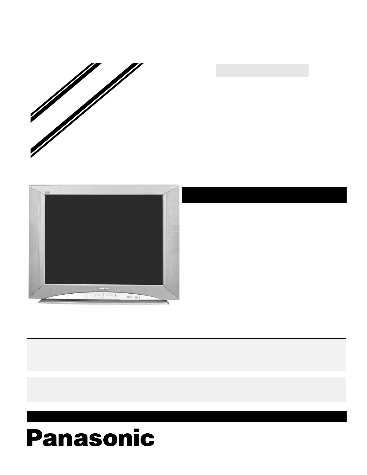
Panasonic
Models
CT-36HL42F AP388
CT-36HL42UF AP388
CT-36HL42CF AP388
This Simplified Service Manual is issued to add listed models to the Main Service Manual order No. MTNC020618C1
(CT36HX42F) of the DX3P family. A set of schematics, unique settings and a complete parts list are included in this
Manual.
Please file and use this Simplified Service Manual together with Main Service Manual order No. MTNC020618C1.
Chassis
“WARNING! This Service Manualis designed for experiencedrepairtechniciansonlyand is not designed for useby the generalpublic.
It does not contain warnings or cautions to advise non-technical individuals of potential dangers in attempting to service a product.
Products powered by electricity should be serviced or repaired only by experienced professional technicians. Any attempt to
service or repair the product or products dealt with in this Service Manual by anyone else could result in serious injury or death.”
The service technician is requiredtoreadand follow the “Safety Precautions”and“Important Safety Notice” in this Main Manual.
Copyright 2002by Matsushita Electric Corporation of
America. All rights reserved. Unauthorized copying
®
and distributionis a violation of law.
Page 2
Important safety notice
Special components are used in this television set which are important for safety. These parts are identified on the
schematic diagram by the symbol and printed in BOLD TYPE on the replacement part list. It is essential that
these critical parts are replaced with the manufacturer’s specified replacement part to prevent x-ray radiation,
shock, fire or other hazards. Do not modify the original design without the manufacturer’s permission.
Safety precautions
General guidelines
An Isolation transformer should always be used
during the servicing of a receiver whose chassis is not
isolated from AC power line. Use a transformer of
adequate power rating as this protects the technician
from accidents resulting in personal injury from
electrical shocks. It will also protect the receiver from
being damaged by accidental shorting that may occur
during servicing.
When servicing, observe the original lead dress,
especially in the high voltage circuit. Replace all
damaged parts (also parts that show signs of
overheating.)
Always replace protective devices,suchas
fishpaper, isolation resistors and capacitors, and
shields after servicing the receiver. Use only
manufacturer’s recommended rating for fuses, circuits
breakers, etc.
High potentials are present when this receiver is
operating. Operation of the receiver without the rear
cover introduces danger for electrical shock. Servicing
should not be performed by anyone who is not
thoroughly familiar with the necessary precautions
when servicing high-voltage equipment.
Extreme care should be practiced when handling the
picture tube. Rough handling may cause it to implode
due to atmospheric pressure. (14.7 lbs per sq. in.). Do
not nick or scratch the glass or subject it to any undue
pressure. When handling, use safety goggles and
heavy gloves for protection. Discharge the picture
tube by shorting the anode to chassis ground (not to
the cabinet or to other mounting hardware). When
discharging connect cold ground (i.e. dag ground lead)
to the anode with a well insulated wire or use a
grounding probe.
Avoid prolonged exposure at close range to unshielded
areas of the picture tube to prevent exposure to
x-ray radiation.
The test picture tube used for servicing the chassis at
the bench should incorporate safety glass and
magnetic shielding. The safety glass provide shielding
for the tube viewing area against x-ray radiation as well
as implosion. The magnetic shield limits the x-ray
radiation around the bell of the picture tube in addition
to the restricting magnetic effects. When using a
picture tube test jig for service, ensure that the jig is
capable of handling 50.0kV without causing
x-ray radiation.
Before returning a serviced receiver to the owner,
the service technician must thoroughly test the unit to
ensure that is completely safe to operate. Do not use a
line isolation transformer when testing.
Leakage current cold check
Unplug the AC cord and connect a jumper between the
two plug prongs.
Measure the resistance between the jumpered AC plug
and expose metallic parts such as screwheads,
antenna terminals, control shafts, etc. If the exposed
metallic part has a return path to the chassis, the
reading should be between 240kΩ and 5.2MΩ. If the
exposed metallic part does not have a return path to
the chassis, the reading should be infinite.
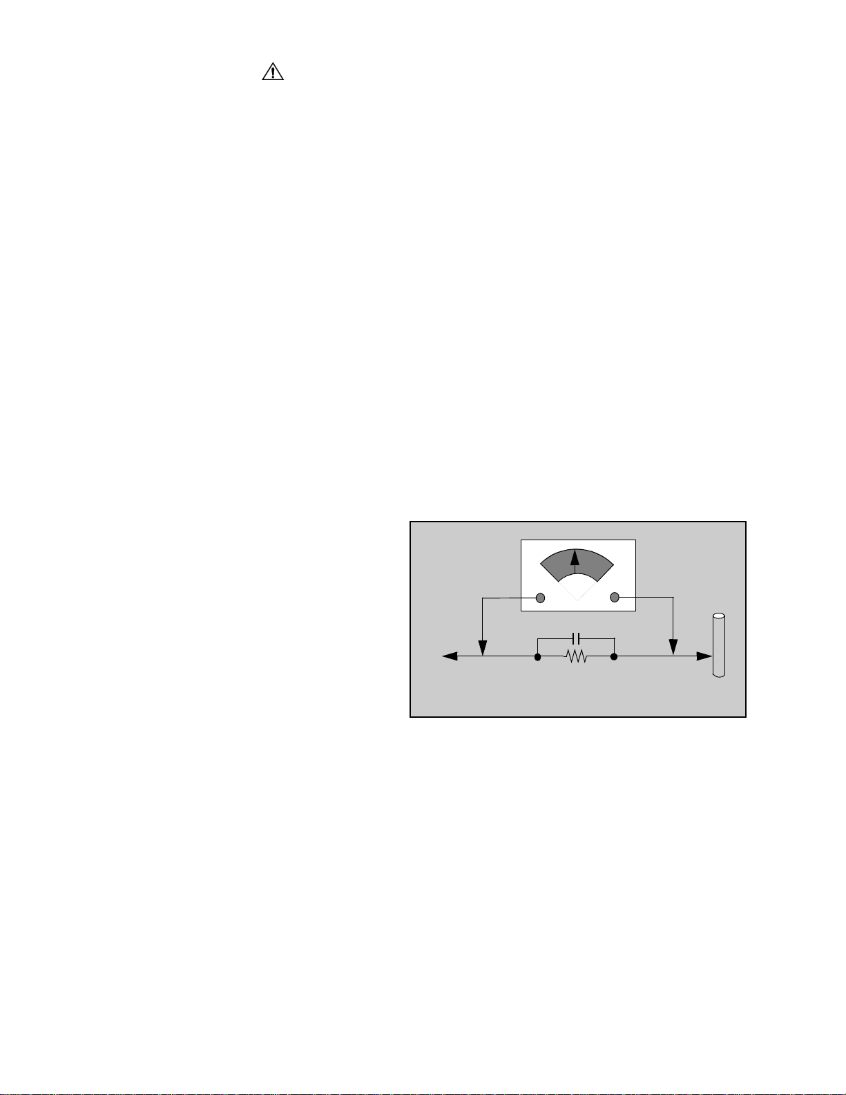
Leakage current hot check (Fig. 1)
Plug the AC cord directly into the AC outlet. Do not use
an isolation transformer during the check.
Connect a 1.5kΩ 10 watt resistor in parallel with a
0.15µF capacitor between an exposed metallic part
and ground. Use earth ground, for example a
water pipe.
Using a DVM with a 1000 ohms/volt sensitivity or
higher, measure the AC potential across the resistor.
Repeat the procedure and measure the voltage
present with all other exposed metallic parts.
Verify that any potential does not exceed 0.75 volt
RMS. A leakage current tester (such a Simpson model
229, Sencore model PR57 or equivalent) may be used
in the above procedure, in which case any current
measure must not exceed 0.5 milliamp. If any
measurement is out of the specified limits, there is a
possibility of a shock hazard and the receiver must be
repaired and rechecked before it is returned to the
customer.
AC VOLTMETER
COLD
WATER
PIPE
(GROUND)
0.15µF
TO INSTRUMENT’S
EXPOSED METAL
PARTS
1500Ω,10 W
Figure 1. Hot check circuit
X-ray radiation
WARNING: The potential source of x-ray radiation in the
TV set is in the high voltage section and the picture tube.
Note: It is important to use an accurate,
calibrated high voltage meter.
Set the brightness, picture, sharpness and color
controls to minimum.
Measure the high voltage. With a 480i signal the high
voltage should be 33.0kV (± 1.0kV) and with a 1080i
signal the high voltage should be 33.0kV (+1.0kV,
-2.0kV). If the upper limit is out of tolerance,immediate
serviceandcorrectionisrequiredtoinsuresafe
operation and to prevent the possibility of premature
component failure.
Horizontal oscillator disable circuit test
This test must be performed as afinal check before the
receiver is returned to the customer. See horizontal
oscillator disable circuit procedure check in
this manual.
-2-
Page 3
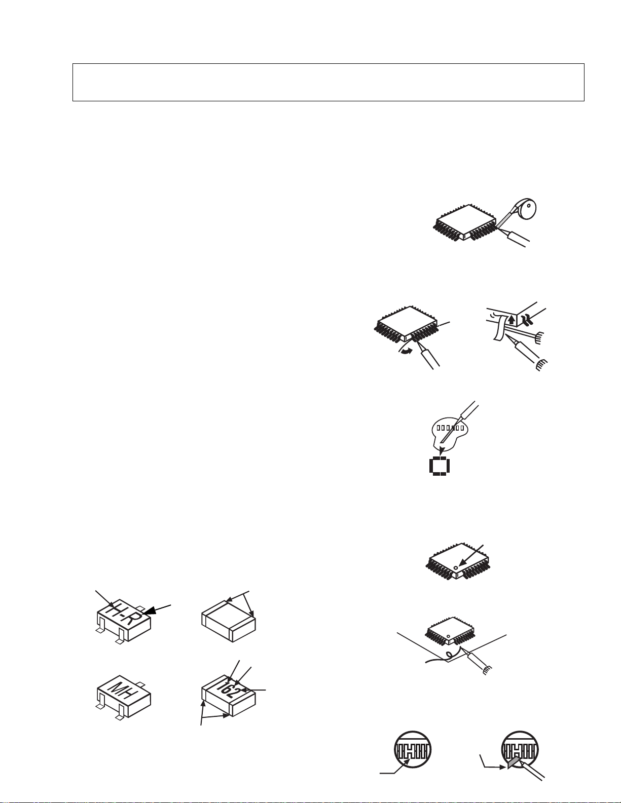
Service notes
Note: These components are affixed with glue. Be careful not to break or damage any foil under
the component or at the pins of the ICs when removing. Usually applying heat to the
component for a short time while twisting with tweezers will break the component loose.
Leadless chip component
(surface mount)
Chip components must be replaced with identical chips
due to critical foil track spacing. There are no holes in
the board to mount standard transistors or diodes.
Some chips capacitor or resistor board solder pads
may have holes through the board, however the hole
diameter limits standard resistor replacement to 1/8
watt. Standard capacitor may also be limited for the
same reason. It is recommended that identical
components be used.
Chip resistor have a three digit numerical resistance
code - 1st and 2nd significant digits and a multiplier.
Example: 162 = 1600 or 1.6kΩ resistor, 0 = 0Ω (jumper).
Chip capacitors generally do not have the value
indicated on the capacitor. The color of the component
indicates the general range of the capacitance.
Chip transistors are identified by a two letter code. The
first letter indicates the type and the second letter, the
grade of transistor.
Chip diodes have a two letter identification code as per
the code chart and are a dual diode pack with either
common anode or common cathode. Check the parts
list for correct diode number.
Component removal
1. Use solder wick to remove solder from component
end caps or terminal.
2. Without pulling up, carefully twist the component
with tweezers to break the adhesive.
3. Do not reuse removed leadless or chip
components since they are subject to stress
fracture during removal.
Chip component installation
1. Put a small amount of solder on the board
soldering pads.
2. Hold the chip component against the soldering
pads with tweezers or with a miniature alligator clip
and apply heat to the pad area with a 30 watt iron
until solder flows. Do not apply heat for more than
3 seconds.
TYPE
Chip components
GRADE
c
SOLDER
CAPS
How to replace Flat-IC
- Required tools -
• Soldering iron • De-solder braids
• Iron wire or small awl • Magnifier
1. Remove the solder from all of the pins of a Flat-IC
by using a de-solder braid.
De-Solder
Flat-IC
2. Put the iron wire under the pins of the Flat-IC and
pull it in the direction indicated while heating the
pins using a soldering iron. A small awl can be
used instead of the iron wire.
Iron
Wire
Pull
Soldering
Iron
Soldering
Iron
3. Remove the solder from all the pads of the Flat-IC
by using a de-solder braid.
Soldering
Iron
De-Solder
Braid
Flat IC
4. Position the new Flat-IC in place (apply the pins of
the Flat-IC to the soldering pads where the pins
need to be soldered). Properly determine the
positions of the soldering pads and pins by
correctly aligning the polarity symbol.
First pin
123.....
5. Solder all pins to the soldering pads using a fine
tipped soldering iron.
Braid
Awl
b
ANODES
MH DIODE
e
TRANSISTOR
COMMON
CATHODE
SOLDER
CAPS
CAPACITOR
1ST DIGIT
RESISTOR
2ND DIGIT
MULTIPLIER
=1600 = 1.6k
Soldering
Solder
iron
6. Check with a magnifier for solder bridge between
the pins or for dry joint between pins and soldering
pads. To remove a solder bridge, use a de-solder
braid as shown in the figure below.
De-Solder
braid
Solder
bridge
Soldering
iron
-3-
Page 4

About lead free solder (PbF)
Note: Lead is listed as (Pb) in the periodic table of elements.
In the information below, Pb will refer to Lead solder, and PbF will ref er to Lead Free Solder.
The Lead Free Solder used in our manufacturing process and discussed below is (Sn+Ag+Cu).
That is Tin (Sn), Silver (Ag) and (Cu) although other types are available.
This model uses Pb Free solder in it’s manufacture due to environmental conservation issues. For
service and repair work, we’d suggest the use of Pb free solder as well, although Pb solder may be
used.
PCBs manufactured using lead free solder will have the “PbF” or a leaf symbol stampedon the
back of PCB.
Caution
• Pb free solder has a higher melting point than standard solder. Typically the melting
point is 50 ~ 70 °F(30~40°C) higher. Please use a high temperature soldering iron
and set it to 700 ± 20 °F(370± 10 °C).
• Pb free solder will tend to splash when heated too high (about 1100 °For600°C).
If you must use Pb solder, please completely remove all of the Pb free solder on the
pins or solder area before applying Pb solder. If this is not practical, be sure to heat the
Pb free solder until it melts, before applying Pb solder.
• After applying PbF solder to double layered boards, please check the component side
for excess solder which may flow onto the opposite side. (see figure below)
remove all of the
excess solder
component
pin
component
slice view
solder
Suggested Pb free solder
There are several kinds of Pb free solder available for purchase. This product uses Sn+Ag+Cu
(tin, silver, copper) solder. However, Sn+Cu (tin, copper), Sn+Zn+Bi (tin, zinc, bismuth) solder
canalsobeused.
0.3mm X 100g
0.6mm X 100g 1.0mm X 100g
-4-
Page 5

Importantsafetynotice................... 2
Safetyprecautions................. 2
Generalguidelines................. 2
Leakage current cold check . . . . . . . . . . 2
Leakage current hot check . . . . . . . . . . . 2
X-rayradiation .................... 2
Horizontal oscillator disable circuit test. . 2
Servicenotes........................... 3
Leadless chip component
(surfacemount)................ 3
Componentremoval................ 3
Chip component installation . . . . . . . . . . 3
HowtoreplaceFlat-IC.............. 3
About lead free solder (PbF) .............. 4
HHSreferenceadjustment........... 6
Horizontal oscillator disable circuit . . . . . 6
Receiverfeaturetable.................... 7
Boarddesignation....................... 8
Locationofcontrols(receiver)............. 9
Quick reference control operation . . . . . 9
Remote-locationofcontrols............. 10
Auto diagnosis feature . . . . . ............. 11
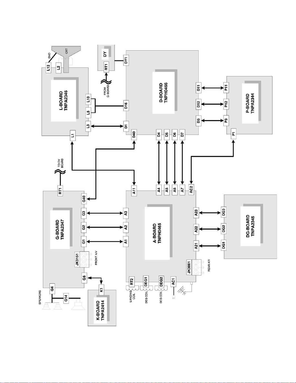
Boardconnections..................... 15
Description of connectors . . . . . . . . . . ..... 16
Identification of components . . . . . . . . ..... 18
Partslist.............................. 24
Partslistabbreviations.................. 35
Foldoutsnotes......................... 36
Schematics & v oltages
G-Boardschematic................ 38
G-Boardvoltages................. 41
K-Boardschematic................ 42
Layouts
G-PCB ......................... 44
K-PCB.......................... 46
Disassemblyforservice................. 12
Backcover...................... 12
A-Board-Mainchassis ............ 12
L-Board-CRToutput.............. 12
DG-Board ...................... 12
P-Board ........................ 12
G-Board........................ 12
K-Board ........................ 13
Speakers ....................... 13
Disassembly for CRT replacement . . . . . . . . 13
CRTreplacement................. 13
Backcoverremoval..................... 14
-5-
Page 6
Service notes (continued)
IMPORTANT: To protect against possible damage to
the solid state devices due to arcing or static discharge,
make certain that all ground wires and CRT DAG wire
are securely connected.
CAUTION: The power supply circuit is above earth
ground and the chassis cannot be polarized. Use an
isolation transformer when servicing the receiver to
avoid damage to the test equipment or to the chassis.
Connect the test equipment to the proper ground
(hot ) or (cold ) when servicing, or incorrect
voltages will be measured.
WARNING: This receiver has been designed to meet
or exceed applicable safety and x-ray radiation
protection as specified by government agencies and
independent testing laboratories.
To maintain original product safety design standards
relative to x-ray radiation and shock and fire hazard,
parts indicated with the symbol on the schematic
must be replaced with identical parts. Order parts from
the manufacturer’s parts center using the parts
numbers shown in this service manual, or provide the
chassis number and the part reference number.
For optimum performance and reliability, all other parts
should be replaced with components of
identical specification.
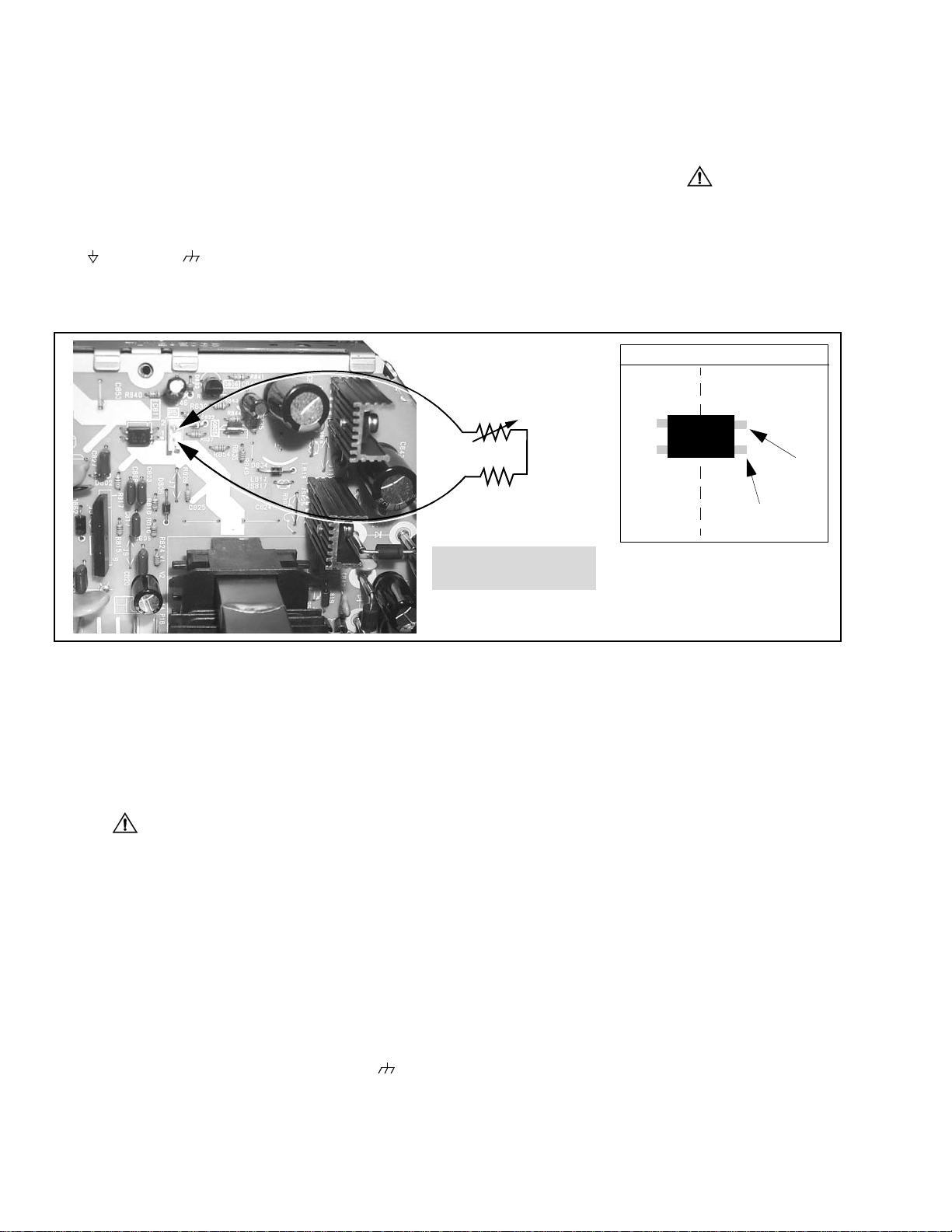
Alternative test points
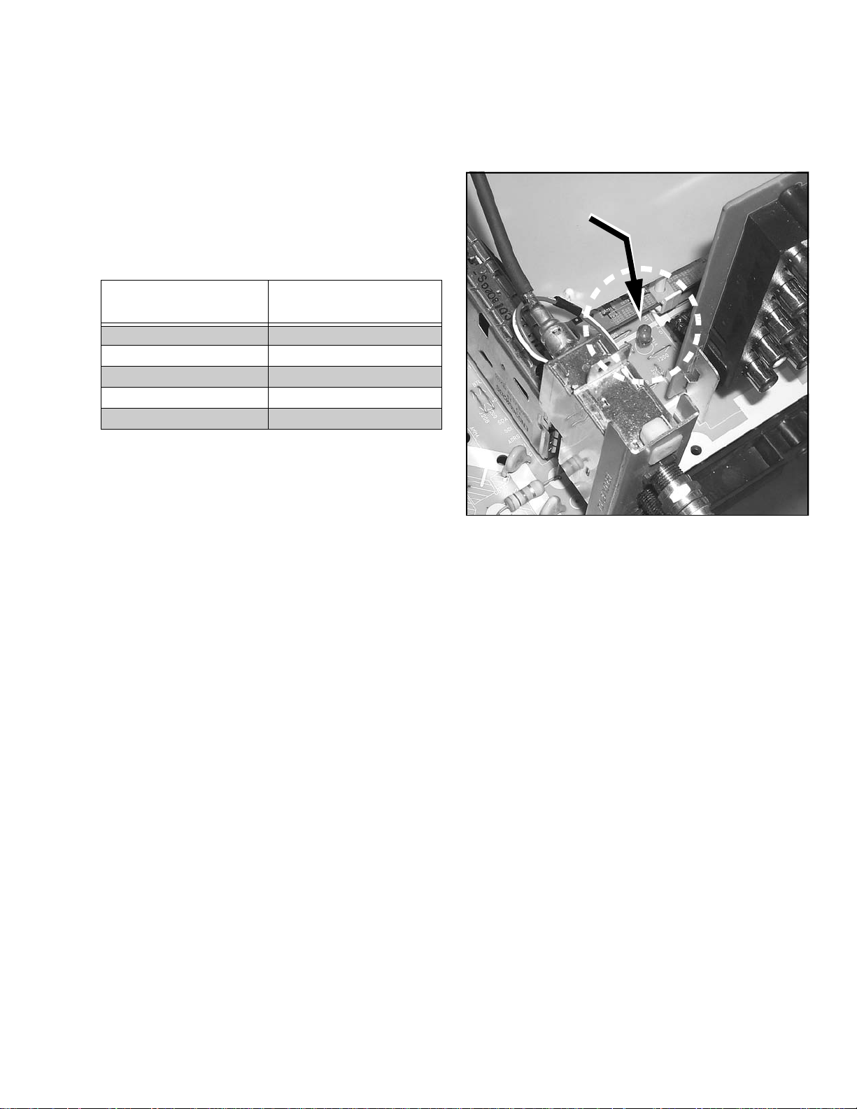
Horizontal oscillator disable circuit
This chassis employs a special circuit to protect
against excessive high voltage and beam current. If, for
any reason, the high voltage and beam current exceed
a predetermined level this protective circuit activates
and detunes the horizontal oscillator that limits the high
voltage. The over-voltage protection circuit is not
adjustable. However, if components indicated by the
symbol on the schematic in either the horizontal
sweep system or the over-voltage protection circuit
itself are changed, the operation of the circuit should be
checked using the following procedure:Equipment
needed to check the disabled circuit:
1. High voltage meter (0- 50kV)
2. Variac or isolation transformer
3. 1k ohm VR
4. DC Ammeter
Preparation
1. Connect receiver to AC 120 Volts. Do not turn ON.
2. Connect HIGH VOLTAGE meter to 2nd anode
(H.V. button).
negative lead.
3. Connect the ammeter serial from the flyback anode
lead to the picture tube anode socket.
4. Prepare HHS jig to be connected between TPD50
and TPD51 on P-Board as shown above.
Note:Use cold ground ( ) for
TPD51 (P5-2)
1kΩ
HOT
GROUND
COLD
GROUND
HHS Jig
IC811
100Ω
TPD50 (P5-1)
(OPTO)
TPD51
(Led cathode)
TP labels are located
on bottom of board
Figure 2. Power supply jig detail (D-Board)
Procedure
:
1. Open connector A17.
2. Turn power ON and apply a white pattern.
3. Set current within 50-100µΑ
by changing the
picture and bright controls.
4. Turn power OFF.
5. Connect HHS jig between TPD50 and TPD51 on
P-Board as shown above (VR should be turn fully
clockwise).
6. Turn power on.
7. Using the variable resistor slowly increase the
current until the horizontal sync frequency abruptly
increases indicating that the horizontal frequency is
just beginning to pull out of sync. Maintain the
current within
50-100µΑ by changing the picture
and bright controls
8. Observe the high voltage meter. High voltage
should read less than 38.4kV.
9. Turn power OFF, remove HHS jig, HV meter,
ammeter and connect A17 connector.
10. Turn power ON. Reset PICTURE and
BRIGHTNESS controls. Confirm B+ 144V±1.5V
with 120V AC applied.
Note: If high voltage is not within the
specified limit the cause must be
determined before the receiver is
returned to the owner.
-6-
TPD50
(Led anode)
Page 7
Receiver feature table
FEATURE\MODEL CT-36HL42F/UF/CF
Chassis DX3P
Number of channels 181
Menu language ENG/SPAN/FR
Closed caption X
V-Chip (USA/CANADA) X
Picture in Picture PIP 2T
2RF X
Remote model number EUR7603Z30
Picture tube A90LSW295X
PureFlat PF (4:3)
Comb ADV 3D Y/C
VM X(DIGITAL)
Color Temp X
V/A norm (X=both) X
MTS/SAP/DBX X
Built-in audio power 10W x 3
Number of speakers 2 w/subwoofer
Bass/Bl/Treble Control X
AI Sound X
SURROUND/BBE X
A/V in (rear/front) 4(3/1)
A/V Prog out X
Component Input 2
Audio Out (FAO,VAO) F,V
S-VHS input (rear/front) 2/1
EPJ/HPJ/MISC HPJ
Dimensions mm
(HxWxD) in
Weight (kg/lbs) 98/216.05
Power source (V/Hz) 120/60
Anode voltage
Video input jack
Audio input jack 500mV RMS 47kΩ
891x1094x742
35.07x43.07x29.21
31.0kV
1V
± 1.0kV
75Ω phono jack
p-p
Table 1. Receiver features
Specifications are subject to change without notice or obligation.
Dimensions and weights are approximate.
-7-
Page 8
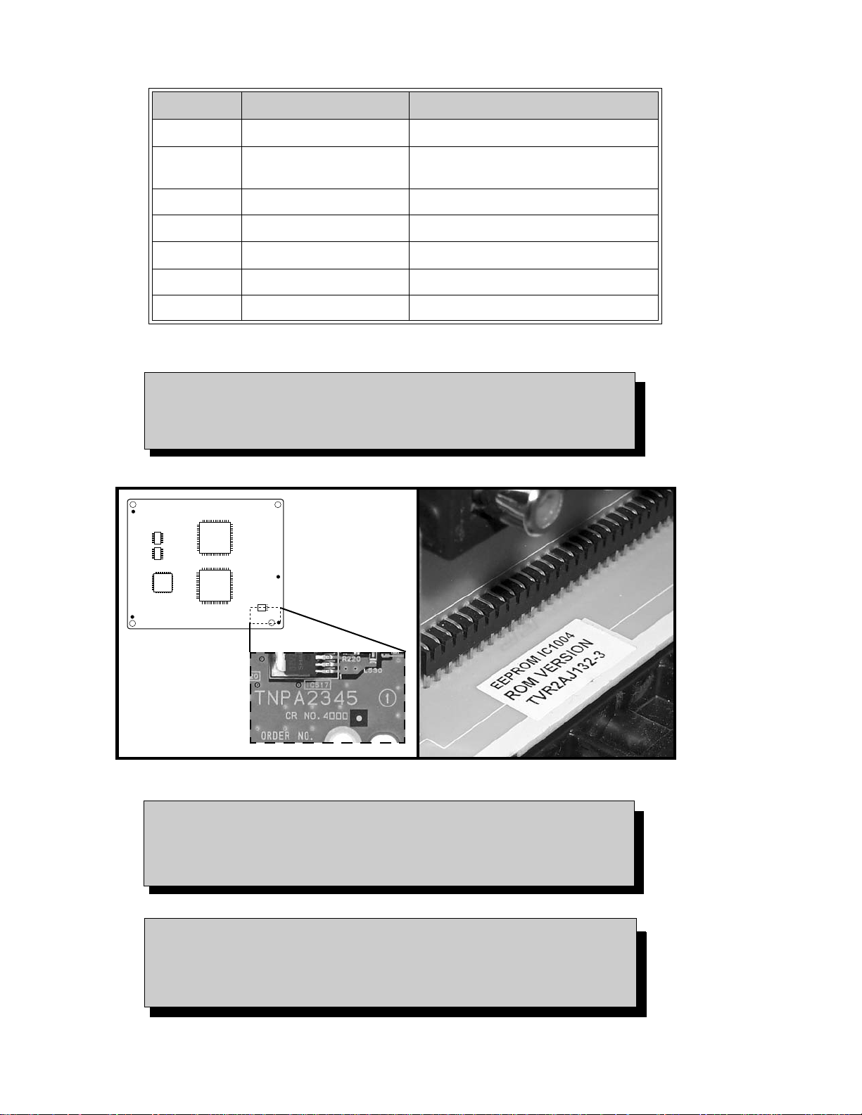
Board designation
Board Board number Description
A-Board TNPH0465 Main panel
DG-Board**
L-Board TNPA2346 CRT board
D-Board TNPH0466 High voltage and deflection panel
P-Board TNPA2344 Power supply panel
G-Board TNPA2347 Front A/V inputs, speaker conectors.
K-Board TNPA2414 Keyboard, LED and IR Sensor Panel.
** IMPORTANT:
TNPA2345/
TNPA2345AC
MPU, Digital video board, PIP processing,
Since two different versions of DG-boards are available for
the CT-36HL42 models, please check board number printed on the lower
right corner (fig. 3a) when replacing DG-Board. Refer to label on chassis for
EEPROM p art number that is used (see fig. 3b for label location).
Panasonic
Panasonic
TNPA2345
Top side
a)
Figure 3. a)DG-Board number location b)EEPROM label on A-Board below A/V jacks.
Note: The DG-Board (TNPA2345 or TNPA2345AC) is non-serviceable.
If this board is defective replace it with a new one. Each version of
DG-Board must be matched with correct version of EEPROM.
Confirm the EEPROM part number before replacing.
Notice: When ordering any board, add and ” S” after the board suffix
application.
Example: If ordering D-Board, should be ordered as:
b)
TNPH0466
S.
-8-
Page 9
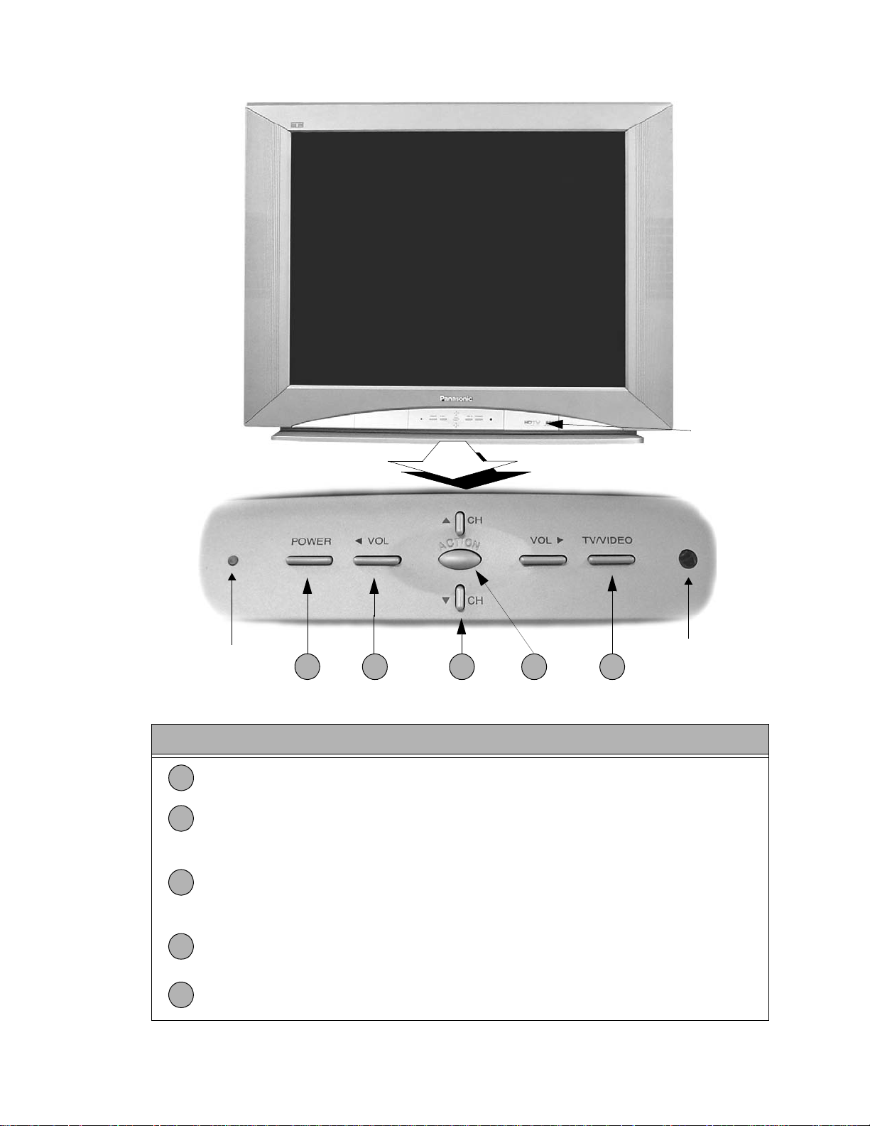
Location of controls (receiver)
A/Vinputsinside
front door
LED
1
2 4 53
Remote control
sensor
Figure 4. Location of controls receiver
Quick reference control operation
1
POWER button - Press to turn ON or OFF.
VOLUME buttons - Press to adjust sound level, or to adjust audio menus, video
2
menus, and select operating features when menus are displayed
CHANNEL buttons - Press to select programmed channels. Press to highlight desired
features when menus are displayed. Also use to select cable converter box channels
3
after programming remote control infrared codes (the TV/AUX/CABLE switch must be
set in CABLE position).
ACTION button - Press to display main menu and access on screen feature and
4
adjustment menus.
TV/VIDEO button - Press to select TV or one of two video inputs, for the main picture
5
or the PIP frame (when PIP frame is displayed).
-9-
Page 10

Remote - location of controls
POWER button
Press to turn ON and OFF.
MUTE button
Press to mute sound.
A second press resumes sound. Press also to
access and delete Closed Caption display.
TV, VCR, DVD, DTV,AUX, CBL,RCVR, DBS
buttons
Component function buttons
VOL (volume) buttons
Press to adjust TV sound level. Use with
channel buttons to navigate in menus.
R-TUNE (rapid tune) button.
Press to switch to theprevious
channel.
ACTION button
Press to display main menu and access or exit
On Screen features and Adjustment Menus.
REW,PLAY, FF, TV/VCR, STOP, PAUSE, REC
& VCR CHANNEL buttons
Component function buttons.
DBS EXIT& DBS GUIDE buttons
DBS function buttons.
LIGHT button
Press to light remote control buttons.
SAP button
Access secondary audio program
ASPECT button
Select picture size (ratio) to match
programmingformat (DTV-STB and DBS only).
PROG button
Press to enter minor number in a compound
number.
MOVE, PIP, SPLIT/SIZE, FREEZE, SWAP,
SEARCH, PIP CHANNEL, PIP MIN, PIP MAX
PIP function buttons.
Figure 5. Location of controls (EUR7603Z30 remote)
For additional information for this remote please refer to the owner’s
manual section remote operation, part number listed on parts list section.
-10-
Page 11
Auto diagnosis feature
This receiver incorporates a new auto-diagnosis
feature. With this new feature will be easier for the
repair technician to detect the failures. There is a LED
located on the A-Board by the DG-Board, this LED will
start flashing when a failure is detected by the circuits
located in a specific area, depending on how many
times the LED is flashing, this will tell you what circuit
should be checked.
After the count:
Proceed to check that area, verify what board is the
problem located, this way the area to check will be
reduced until the failure is found.
Make a count of flashing and see Table 1.
Please use this feature effectively especially for
intermittent problems.
NUMBER OF
FLASHES
1 +140 (POWER)
2LOWDC(+B)
4 HHS (HIGH VOLTAGE)
5IC4511
6 IC4518
Table 1: SOS of diagnosis LED
Refer to Fig. 6 for DIAGNOSIS LED location.
POSSIBLE CIRCUIT
LED
Figure 6. Diagnosis LED location
-11-
Page 12
Disassembly for service
Back cover
Remove all the screws marked with an arrow( )
from the back of the receiver (see Fig. 12):
• 4 screws at the top edgeof the receiver.
• 3 screw by the A/V jacks.
• 1 screw by the RF jacks.
• 1 screw at each lower corner of the receiver.
• 1 screw by the retainer plate of the AC power cord.
• 1 screw at each lower side of the receiver.
• 1screw below the A/V jacks
Note: Extensions for board connectors may
be needed to test voltages on
P-Board, please see parts list section
for part numbers in this service
manual.
A-Board - Main chassis (see Fig. 14)
The DG-Board is assembled on the main chassis
(A-Board). The A-Board assembly rest on a chassis
tray along with the D-Board.
Slide chassis tray out. Gently lift, tray and pull out.
Disconnect plug connectors; release wire ties and
holders as required for complete chassis removal.
A. A-Board is secured to the chassis tray with five
screws.
B. The D-Board is secured to the chassis tray with
three screws
C. The A-Board is mated to the D-Board by four
flexible connectors: A4, A5, A6 & A7 (D4, D5, D6 &
D7 on the D-Board, respectively). To remove either
boards, unplug the connectors on the A-Board.
Note: Some tie-wraps that secure the wire
dressings may need to be unfastened
for chassis removal.
Insert wire then
pull upwards
Note: To realease the
GND cable from
D13 connector
insert a wire in
both cavities of
connector, then
pull up the
cable.
Figure 7. D-Board D13 GND connector.
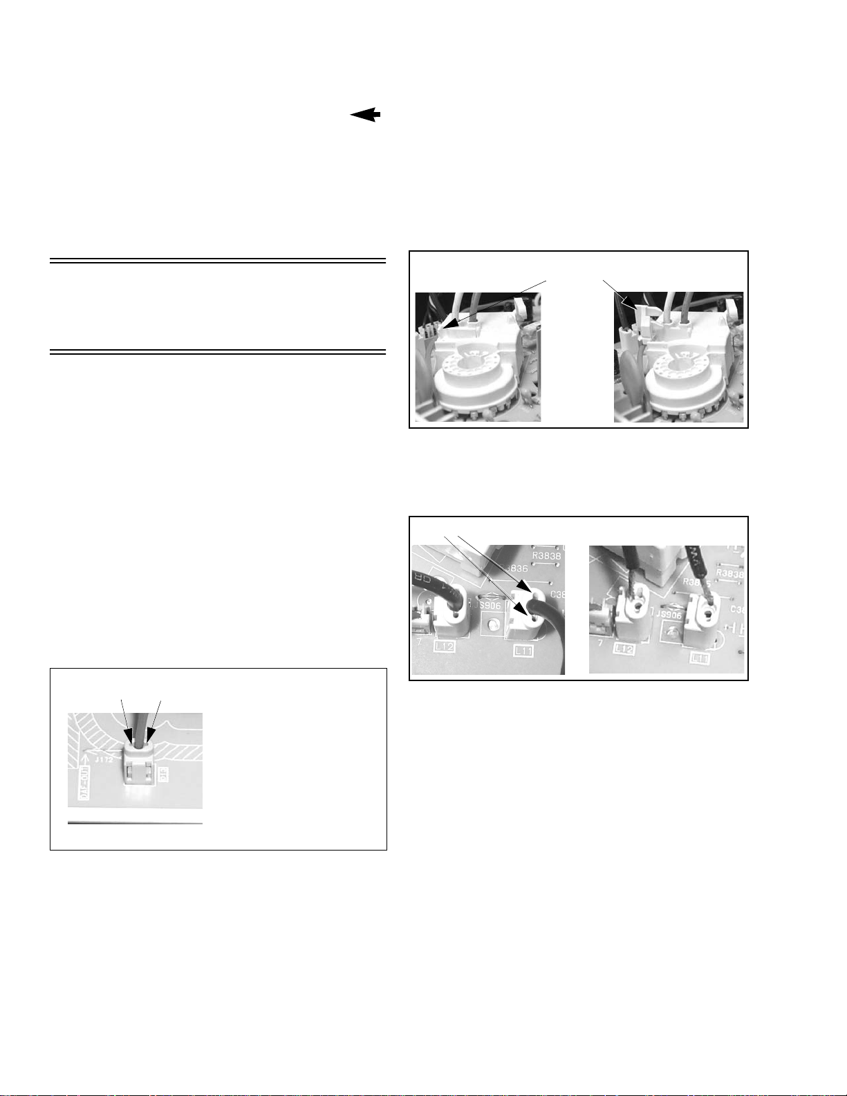
L-Board - CRT output
Plugs into the socket on the CRT neck.
To remove this board, first unplug the board from
the CRT neck, then disconnect L1, L2 and L3
connectors, to disconnect the focus F1(red cable)
& F2 (white cable) cables, pull the tab and release
the cables (see Fig. 8), finally disconnect the
screen cable from the D-Board D16 (screen and
heater).
To reinsert back the cables, remember the original
position of cables, F1 (red cable) goes to A on the
CRT socket and F2 (white cable) goes to B on the
CRT socket.
Figure 8. F1 & F2 cables release
To release screen GND cables from L-Board L11 &
L12 connectors, insert a wire in both sides of connector
and pull upwards the cable, then remove the wire
(see Fig. 9)
Insert wire
Figure 9. L-Board screen GND cables release
Press tab
leftward to
release cables
Pull cables
upwards
Pull cables upwards
DG-Board
Plugs onto the A-Board at the A21, A22 and A23
(DG21, DG22 and DG23 respectively) connectors.
Note: This board is not-serviceable.
When removing this board pull carefully.
P-Board
Plugs onto the right side of the D-Board at D3, D2,
D11 & D12 connectors (P3, P2, P11 & P12 on
P-Board, respectively); First remove the three
screws that holds the metal board, one from the
flyback and two from the chassis tray and then use
a flat head screwdriver to release the connector
locking tabs and pull upwards the board.
-12-
G-Board
Mated to A-Board by three flexible connectors (A1,
A2, A3) and D-Board by one flexible connector
(D40). To remove this board, first unplug the four
flexible connectors, then RT4 and G4 connectors,
then pull upwards the board while unlock the tabs
from the chassis tray.
Page 13
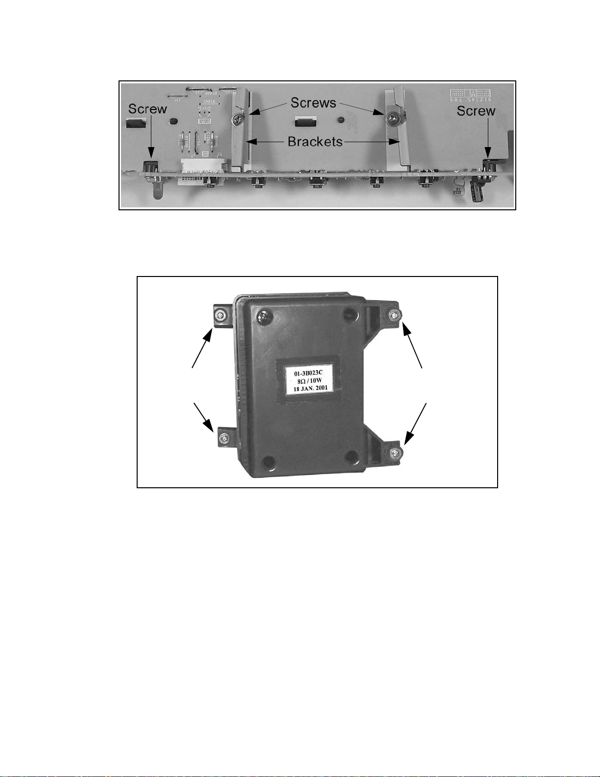
K-Board
Is fastened to the G-Board by two metal brackets that are secured by a screw (each one). Plugs into the front
of G-Board by connector K1 to G6,and is fastened to the chassis tray assembly by 2 screws on each lower
corner.(Fig. 9).
G-Board
K-Board
Figure 10. K-Board toG-Board Assembly (Top View).
Speakers
Each speaker is secured to a plastic base with 4 screws, and each plastic base is secured to a second base
with two screws, and assembled to the cabinet with two screws.
The subwoofer speaker is assembled within the backcover of the television set by 4 screws (Fig. 10).
Screws secured
to back cover
Figure 11. Subwoofer speaker
Note: Be sure to reconnect the speaker wires to the correct speaker lead (+) (-)
Screws secured
to back cover
-13-
Page 14
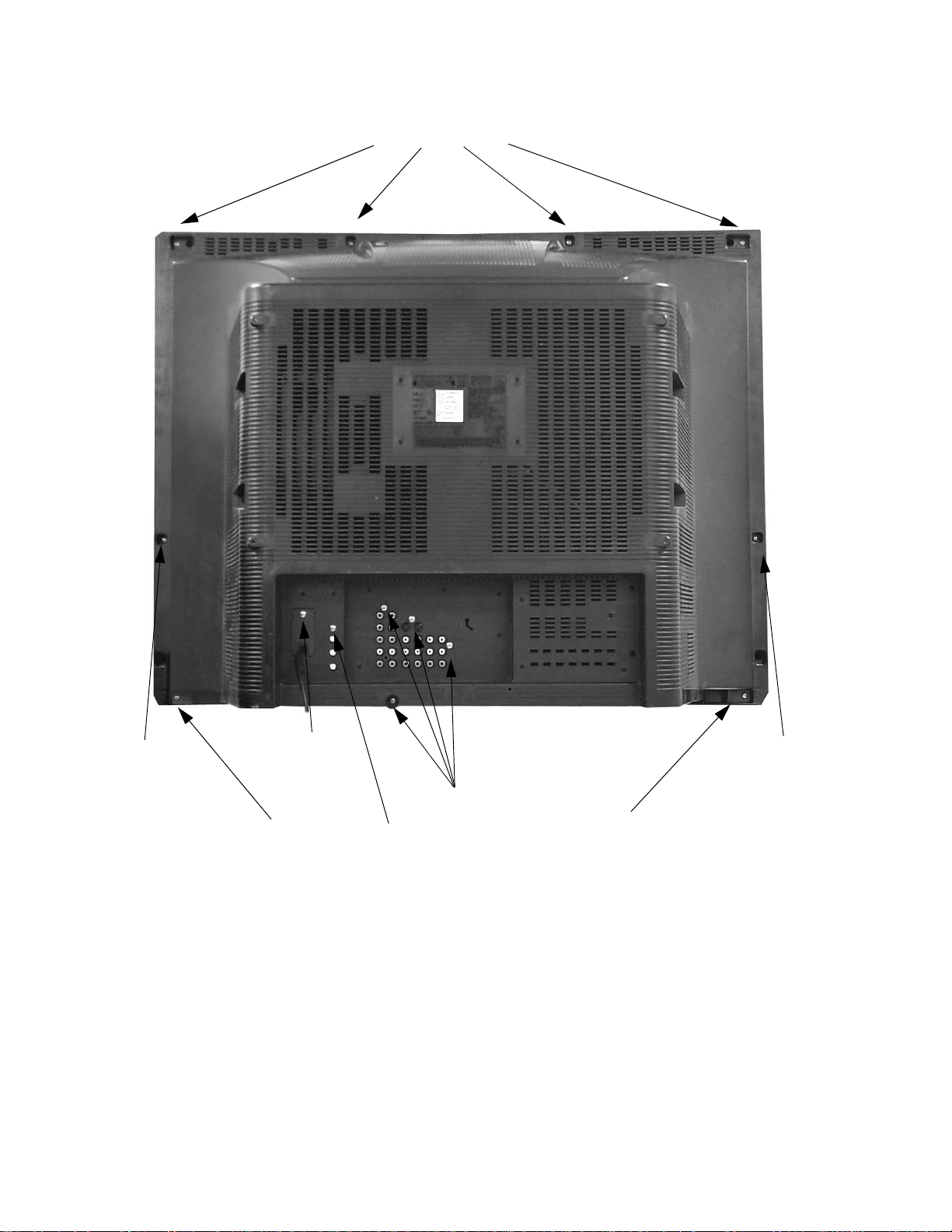
Back cover removal
4screws
at the top edge
1screw
at the lower side
1screwby
the AC cord
1screw
at the lower corner
Figure 12. Back cover removal.
1 screw by
the RF jacks
1screw
at the lower side
4 screws
1screw
at the lower corner
-14-
Page 15
Board connections
Figure 13. Board connections.
-15-
Page 16
Description of connectors
AC2--P1
1
3
5
A15--Factory
1
2
3
4
5
6
7
8
SDA1 (EEPROM)
A12--2RF
1
2
1
2
3
4
5
6
7
8
9
10
1
2
3
4
5
1
2
3
4
5
6
7
8
9
10
AC N.C.
AC +
STB 7V
FA1
FA2 (GND)
SCL1 (EEPROM)
SCL2
SDA2
REMOTE
9V
RF SW
A3--G3
Y4
LV4
V4
RV4
GND
GND
ROUT
RGND
LGND
ROUT
D2--P2
N.C.
N.C.
N.C.
N.C.
N.C.
A2--G2
GND
SDA
SCL
GND
N.C.
HP MUTE
N.C.
AGND
S-4
S2-4 C-4
1
2
3
4
5
6
7
8
9
10
1
2
3
4
5
6
7
8
9
10
11
12
13
14
15
16
17
18
19
20
21
22
23
24
25
26
27
28
29
30
1
2
3
4
5
6
7
8
A1--G1
STB 3.3V
REMOTE
KEY SCAN1
KEY SCAN2
A23--DG3
STB GND
AC SW
DEG SW
AFC 1
AFC 2
LANDING
KEY SCAN 2
KEY SCAN 1
STB 3.3 V
MOMENT B SW
140 SW
V RASTER
HHS DET
HD SD SW
H RASTER
SOS 2
SYSCLK
2RFSW
REMOTE
SP SW
AUDIO MUTE
INPUT MUTE
STB 7V
STB GND
A11--L1
GND
GND
N.C.
9V
12V
GND
SOS
TILT
GND
GND
FA1
N.C.
VM
GND
GND
12 V
GND
A21--DG1
1
2
3
4
5
6
7
8
9
10
11
12
13
14
15
16
17
18
19
20
21
22
23
24
25
26
27
28
29
30
SOS LED
SDA2
SCL2
SDA1
SCL1
N.C.
WP
NTSC VY1
VGND
C1
VGND
NTSC VY2
VGND
C2
VGND
AGND
DTVY2
AGND
PB2
AGND
PR2
AGND
DTVY1
AGND
PB1
AGND
PR1
AGND
STB 3.3V
HHS REF
D10--TESTPIN
1
2
3
4
5
FBP
EHT-DEF
HHS REF
GND
H DRIVE
A7--D7
1
2
3
4
5
6
R
G
B
7
8
9
10
11
12
13
14
15
16
HHS REF
N.C.
N.C.
N.C.
N.C.
N.C.
N.C.
N.C.
ABL
N.C.
VDAF
N.C.
HDAF
N.C.
EHT DET
N.C.
-16-
Page 17
D3--P3
A6--D6
D12--P12
1
2
3
4
5
6
7
8
1
2
3
4
5
6
7
1
2
3
4
5
6
7
8
9
10
11
12
13
14
15
16
17
18
19
20
21
22
23
24
25
26
27
28
29
30
AUDIO -16V
AUDIO -16V
AUDIO GND
AUDIO GND
AUDIO +16V
AUDIO +16V
+B ON/OFF
D1-L3
A22--DG2
MAIN 5V
V DRIVE
H DRIVE
EW DRIVE
EHT DET
SERVICE SW
N.C.
+B 140V
N.C.
- 220V
N.C.
GND
GND
GND
SCL2
SDA2
GND
GND
GND
GND
GND
VM
9V
D2.5V
D2.5V
GND
GND
SUB 5V
N.C.
N.C.
FBP
HDAF
VDAF
ABL
GND
1
2
3
4
5
6
7
8
9
10
11
12
13
14
15
16
HDRIVEGC
VL NEK PRO
FBP
GND
EW DRIVE
GND
GND
N.C.
GND
H RASTER
GND
HD SD SW
GND
HHS DET
GND
GND
A5--D5
1
2
3
4
5
6
7
B
G
R
8
9
10
11
12
13
14
15
16
SERVICEC SW
V DRIVE GC
140V SW ON/OFF
MOMENT B
N.C.
SCL2
SDA2
TILT
GND
V RASTER
GND
GND
SOS
GND
GND
12 V
1
2
3
4
5
6
7
8
1
2
3
4
5
6
7
8
1
2
3
4
5
6
7
8
9
10
UNREG +25V
UNREG +25V
GND
GND
UNREG -15V
GND
UNREG +15V
UNREG +15V
D11--P11
+B 144V
+B 144V
+B 144V
N.C.
N.C.
GND
GND
GND
D40--G40
VSAW
GND
SDA2
GND
SCL2
GND
TILT
+ 15V
GND
- 15V
G6--K1
1
2
3
4
5
6
7
8
9
10
11
12
13
14
15
16
A4--D4
UNREG 15V
UNREG 15V
GND
UNREG 23V
UNREG 23V
GND
BTL 30V
GND
STBY 5V
GND
AUDIO +20V
AUDIO +20V
AUDIO GND
AUDIO GND
AUDIO -20V
AUDIO -20V
1
2
3
4
5
6
7
8
9
10
11
12
STBY 3.3V
5V
STBY 3.3V
5V
KEYSCAN 2
GND
KEYSCAN 1
GND
GND
GND
12VR
RMT
-17-
Page 18

Identification of components
CRT (Secured To Cabinet
By 4 Screws On Corners)
Geomagnetic Coil
Anode
(High Voltage)
D.Yoke
Deg. Coil
L-Board
Speaker
(4 Screws)
Tuners
DG-Board
A/V-Board
A-Board
(main chassis)
Note:
D-Board
After servicing the receiver,remember
to dress the cables, as shown above.
Figure 14. Rear view.
Speaker
(4 Screws)
Flyback
(T551)
P-Board
(power supply)
-18-
Page 19

Identification of components (cont....)
D801
Q801
IC811
P2 P11 P3
RL804
Q806
Q805
D834
P12
T801
IC802
Q952
Figure 15. P-Board
IC3803
Q956
IC3801
Q955
Q951
IC3802
CRT Socket
Figure 16. L-Board
-19-
Page 20
IC515
IC529
IC002
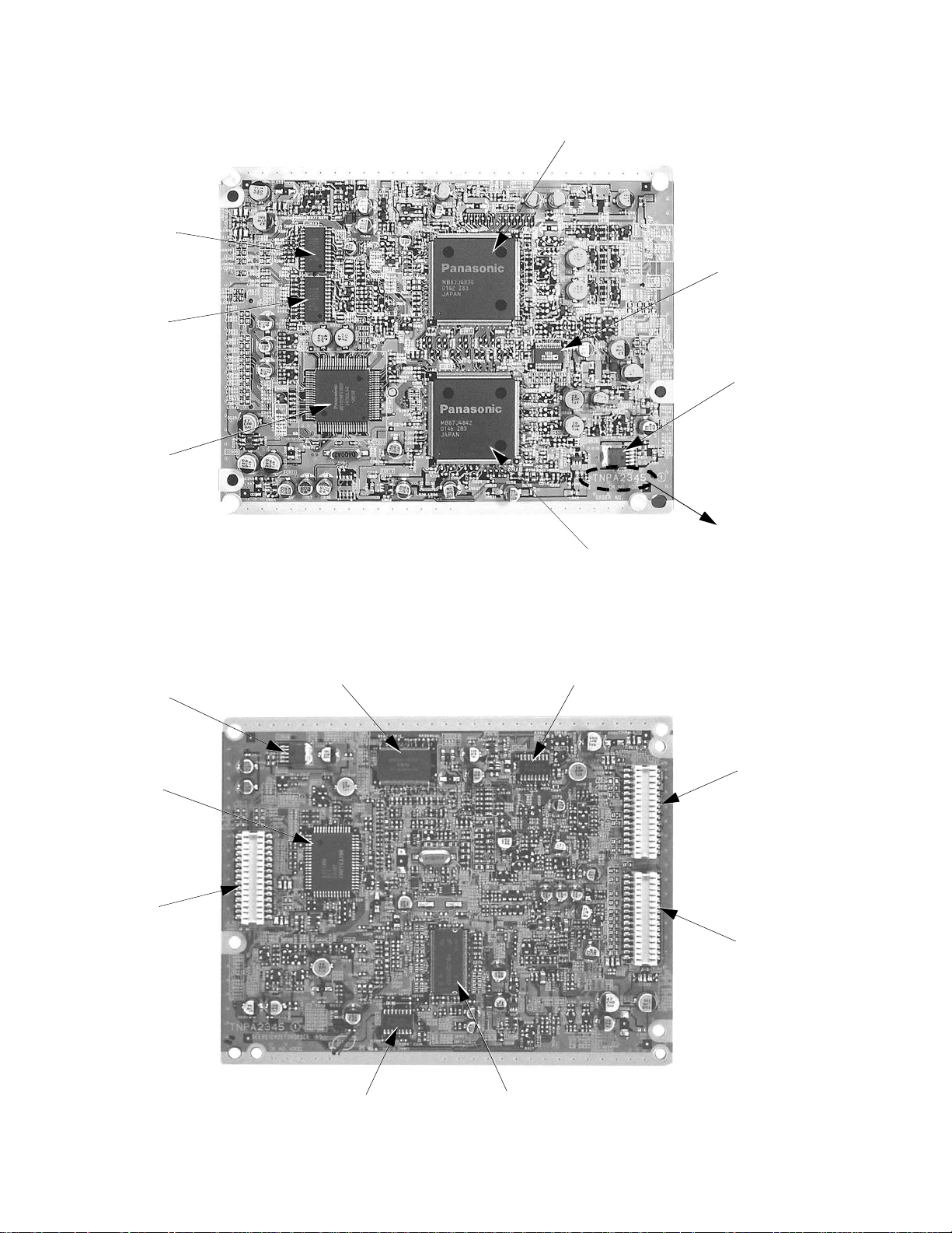
Identification of components (cont....)
IC511
IC506
IC517
IC6502
IC802
DG1
Board Number
IC518
Figure 17. DG-Board top-side
IC507 IC530
DG2
DG3
IC521
Figure 18. DG-Board bottom-side
-20-
IC525
Page 21
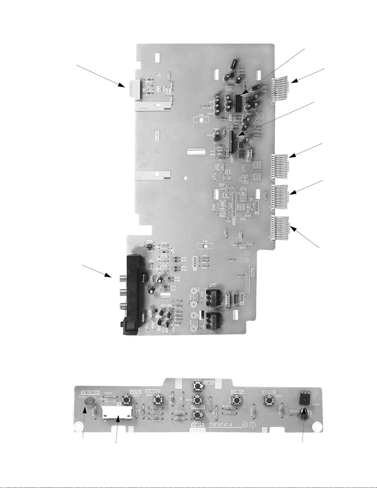
G6
Identification of components (cont....)
IC4805
G40
IC4804
G1
G2
FRONT A/V
G3
Figure 19. G-Board
LED
K1
IR Sensor
Figure 20. K-Board
-21-
Page 22

Identification of components (cont....)
D40
D5
D4
D503
IC500
L554
IC752
RL451
IC451
D3
D12
D6
D7
T1501
D11
Q551
D2
T551
FLY-BACK
Figure 21. D-Board
-22-
Page 23
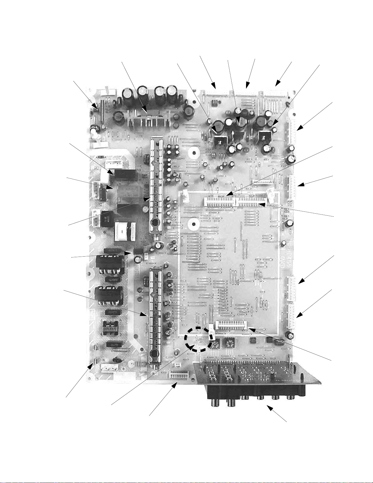
Identification of components (cont....)
IC4803
RL803
RL802
TNR002
IC2302
IC875
A3
IC872
A2
A1
IC871
A4
DG2
A5
DG3
IC804
TNR001
FUSE
DIAGNOSIS
LED
A6
A7
DG1
A15
REAR A/V
Figure 22. A-Board
-23-
Page 24

REPLACEMENT PARTS LIST
Models: CT-36HL42F, CT-36HL42CF, CT-36HL42UF
Important Safety Notice: Components printed in BOLD TYPE have special characteristics important for safety. When
replacingany of thesecomponents use only manufacturer’sspecified parts.
REF NO. PART NO. DESCRIPTION
CAPACITORS
C038 EEUFC1A471B CAP,E 470UF-10V
C039 ECA1HM4R7B CAP,E4.7UF-50V
C040 ECA1VM470B CAP,E 47UF/35V
C041 ECA1HM2R2B CAP,E2.2UF-50V
C042 ECA1VM470B CAP,E 47UF/35V
C043 ECA1HM4R7B CAP,E4.7UF-50V
C044 ECA1VM470B CAP,E 47UF/35V
C045 ECA1HM2R2B CAP,E2.2UF-50V
C047 ECA1HM010B CAP,E1UF-50V
C050 TCJ2VC1H101J CAP,C 100PF-J-50V
C051 TCJ2VC1H101J CAP,C 100PF-J-50V
C058 ECA1HMR22B CAP,E .22UF-50V
C059 ECA1HMR22B CAP,E .22UF-50V
C060 ECA1HM4R7B CAP,E4.7UF-50V
C405 ECA1HM102E CAP,E1000UF-50V
C406 ECQV1H105JL3 CAP,P 1.0UF-J-50V
C407 ECKR1H103ZF5 CAP,C .01UF-Z-50V
C408 ECA1VM102E CAP,E 1000UF-35V
C409 ECA1VM102E CAP,E 1000UF-35V
C411 ECQB1H472JF3 CAP,P 4700PF-J-50V
C412 ECQB1224KF3 CAP,P .22UF-K-100V
C413 ECA1HM010B CAP,E 1UF-50V
C414 ECQB1H272JF3 CAP,P 2700PF-J-50V
C415 ECQB1473KF3 CAP,P .047UF-K-100V
C416 ECQB1H472JF3 CAP,P 4700PF-J-50V
C419 EEUNA1A470B CAP,E 47UF-125V
C420 ECA1CM101B CAP,E100UF/16V
C421 ECA1CM101B CAP,E100UF/16V
C422 ECA1HM010B CAP,E1UF-50V
C434 ECA1HM100B CAP,E10UF/50V
C438 ECQB1H102JF3 CAP,P 1000PF-J-50V
C439 TCJ2VB1H103K CAP,C .01UF-K-50V
C440 ECA1HM100B CAP,E10UF/50V
C457 ECEA1EN4R7UB CAP,E 4.7UF-25V
C501 ECA1VM101B CAP,E 100UF-35V
C502 ECQV1H104JL3 CAP,P .10UF-J-50V
C503 ECKR2H102KB5 CAP,C 1000PF-K-500V
C506 ECA1CM471B CAP,E470UF-16V
C509 ECKR3A222KBP CAP,C .0022UF-K-1KV
C510 TCJ2VC1H221J CAP,C 220PF-J-50V
C511 ECWH20562JVB CAP,P 5600PF-J-2KV
C513 ECQF6103JZH CAP,P .010UF-J-630V
PARTS LIST
C514 ECWH20272JVY CAP,P 2700PF-J-2KV
C515 ECKR3A222KBP CAP,C .0022UF-K-1KV
C516 ECWF2224JSR CAP,M .22UF-J-200V
C517 ECWF2684JSR CAP,M .26UF-J-200V
C518 ECKW3D681KBR CAP,C 680PF-K-2KV
C519 ECKW3D681KBR CAP,C 680PF-K-2KV
C520 ECQB1H183JF3 CAP,P .018UF-J-50V
C521 ECWF2224JSR CAP,M .22UF-J-200V
REF NO. PART NO. DESCRIPTION
C522 ECWH20222JVY CAP,P 2200PF-J-2KV
C523 ECWH20272JVY CAP,P 2700PF-J-2KV
C524 ECQB1224JF3 CAP,P .22UF-J-100V
C525 EEUNA1E220B CAP,E22UF-25V
C526 ECA2EM470E CAP,E 47UF-250V
C527 ECKR2H102KB5 CAP,C 1000PF-K-500V
C528 ECA1HM4R7B CAP,E 4.7UF-50V
C530 ECQE2155JFB CAP,P 1.5UF-J-200V
C531 ECA160V33UE CAP,E 33UF/160V
C532 ECQF6472JZH CAP,P .0047UF-J-630V
C535 ECA1HM471E CAP,E 470UF-50V
C536 ECEA1HN100UB CAP,E 10UF/50V
C537 ECQB1H473JF3 CAP,P .047UF-J -50V
C538 ECA1CM471B CAP,E 470UF-16V
C539 ECA1CM471B CAP,E 470UF-16V
C541 ECQE2333JFB CAP,P .033UF-J-200V
C573 ECQB1H104JF3 CAP,P .10UF-J -50V
C574 ECA1CM470B CAP,E 47UF/16V
C575 ECKR1H103ZF5 CAP,C.01UF-Z-50V
C701 ECQB1H182JF3 CAP,P 1800PF-J-50V
C704 ECQB1H152JF3 CAP,P 1500PF-J-50V
C705 TCJ2VC1H221J CAP,C 220PF-J-50V
C706 ECKW3D271JBN CAP,C 270PF-J-2KVDC
C709 ECQE1106KFB CAP,P 100UF-K-1KV
C712 ECKR1H221KB5 CAP,C 220PF-K-50V
C713 ECKR1H221KB5 CAP,C 220PF-K-50V
C714 ECA1HM2R2B CAP,E 2.2UF-50V
C759 ECQM2104KZW CAP,P .1UF-K-200V
C801 ECQU2A104BN9 CAP,P .10UF-B-250V
C802 ECQU2A823BN9 CAP,P .082UF-B-250V
C803 ECQU2A823BN9 CAP,P .082UF-B-250V
C804 ECQU2A823BN9 CAP,P .082UF-B-250V
C805 ECKW2H472PU7 CAP,C 4700PF-P-500V
C806 ECKW2H472PU7 CAP,C 4700PF-P-500V
C807 ECKW2H472PU7 CAP,C 4700PF-P-500V
C808 ECQB1H102JF3 CAP,P 1000PF-J-50V
C809 ECQB1H333JF3 CAP,P .033UF-J -50V
C810 EC0S2DA821DB CAP,E 820UF-200V
C811 EC0S2DA821DB CAP,E 820UF-200V
C812 ECA1CM471B CAP,E 470UF-16V
C813 ECA1HM010B CAP,E 1UF-50V
C814 ECKW2H472PU7 CAP,C 4700PF-P-500V
C815 ECA1EM471B CAP,E 470UF-25V
C816 ECKW3A272KBP CAP,C 2700PF-K-1KV
C817 ECQB1H332JF3 CAP,P 3300PF-J-50V
C819 TACCQ221T50V CAP,C 220PF/50V
C820 ECA1EHG221B CAP,E 220UF-25V
C821 ECKW3D272KBP CAP,C 2700PF-K-2KV
C822 ECQB1H393JF3 CAP,P .039UF-J -50V
C823 ECQB1H222JF3 CAP,P 2200PF-J-50V
C826 ECA1VM221B CAP,E 220UF-35V
Parts List
-24-
179-02
Page 25

REPLACEMENT PARTS LIST
Models: CT-36HL42F, CT-36HL42CF, CT-36HL42UF.
Important Safety Notice: Components printed in BOLD TYPE have special characteristics important for safety. When replacing
any of these components use only manufacturer’s specified parts.
REF NO. PART NO. DESCRIPTION
C827 ECQB1H333JF3 CAP,P .033UF-J-50V
C828 ECKR3A331KBP CAP,C 330PF-K-1KVDC
C830 EETHC2C102H CAP,E 1000UF-160V
C831 ECKR3A102KBP CAP,C 1000PF-K-1KV
C832 ECA1VHG102E CAP,E 1000UF/35V
C833 ECKR3A471KBP CAP,C 470PF-K-1KV
C834 EEUFC1V222E CAP,E 2200UF-35V
C838 EEUFC1E272E CAP,E 2700UF-25V
C839 ECKR3A151KBP CAP,C 150PF-K-1KV
C840 ECA1EMH471B CAP,E 470UF-25V
C841 ECA1EHG102E CAP,E 1000UF-25V
C842 ECKR3A331KBP CAP,C 330PF-K-1KVDC
C843 ECA1VHG102E CAP,E 1000UF/35V
C844 ECKR3A471KBP CAP,C 470PF-K-1KV
C845 ECA1CM101B CAP,E 100UF/16V
C846 ECA1HM010B CAP,E 1UF-50V
C847 ECA1VM470B CAP,E 47UF/35V
C848 ECA1CM101B CAP,E 100UF/16V
C850 EEUFC1E272E CAP,E 2700UF-25V
C851 ECA1CM221B CAP,E 10UF-16V
C856 ECQU2A103MNB CAP,P .010UF-M-250V
C857 TCJ2VB1H103K CAP,C .01UF-K-50V
C859 ECA1VHG471B CAP,E 470UF-35V
C860 ECKCNA222MEB CAP,C 2200PF-M-125V
C861 ECKCNA222MEB CAP,C 2200PF-M-125V
C876 ECA1EM471B CAP,E 470UF-25V
C877 EEUFC1A471B CAP,E 470UF-10V
C878 ECA1EM221B CAP,E 220UF-25V
C879 EEUFC1A471B CAP,E 470UF-10V
C880 TCJ2VB1H103K CAP,C .01UF-K-50V
C885 ECA1VM471B CAP,E 470UF-35V
C886 EEUFC1C471B CAP,E 470UF-16V
C887 ECA1CM471B CAP,E 470UF-16V
C888 ECA1EM101B CAP,E 100UF-25V
C889 ECA1CM101B CAP,E 100UF/16V
C890 ECA1CM221B CAP,E 10UF-16V
C891 TCJ2VB1H103K CAP,C .01UF-K-50V
C892 ECA0JM221B CAP,E 220UF-6.3V
C893 TCJ2VB1H103K CAP,C .01UF-K-50V
C894 ECA1VM101B CAP,E 100UF-35V
C895 ECA1CM221B CAP,E 10UF-16V
C896 TCJ2VB1H103K CAP,C .01UF-K-50V
C897 ECA1EM471B CAP,E 470UF-25V
C898 TCJ2VB1H103K CAP,C .01UF-K-50V
C899 TCJ2VB1H103K CAP,C .01UF-K-50V
C901 ECQB1H103JF3 CAP,P .01UF-J -50V
C906 ECEA1CN100UB CAP,E 10UF-16V
C952 ECA1CM221B CAP,E 10UF-16V
C953 ECA1CM471B CAP,E 470UF-16V
C955 ECQB1223KF3 CAP,P .22UF-K-100V
C956 ECQE2103KF3 CAP,P .010UF-K-200V
REF NO. PART NO. DESCRIPTION
C957 ECQE2103KF3 CAP,P .010UF-K-200V
C959 ECQB1223KF3 CAP,P .22UF-K-100V
C961 ECA2CM4R7B CAP,E 4.7UF-160V
C962 ECQE2103KF3 CAP,P .010UF-K-200V
C964 ECA1CM101B CAP,E 100UF/16V
C966 ECA1CM101B CAP,E 100UF/16V
C967 ECA2CHG330E CAP,E 33UF-160V
C970 ECQB1H103JF3 CAP,P .01UF-J-50V
C971 ECQB1H103JF3 CAP,P .01UF-J -50V
C973 ECQE2103KF3 CAP,P .010UF-K-200V
C1024 TCJ2VB1H103K CAP,C .01UF-K-50V
C1025 ECA0JM222B CAP,E 2200UF-6.3V
C1051 ECKR1H103ZF5 CAP,C .01UF-Z-50V
C1052 ECA1AM470B CAP,E 47UF-10V
C1504 ECQB1H103JF3 CAP,P .01UF-J-50V
C1505 ECA1CM470B CAP,E 47UF/16V
C1506 TCJ2VF1H102Z CAP,C 1000PF-Z-50V
C1507 ECA1CM220B CAP,E 22UF-16V
C1508 ECKW3D151KBP CAP,C 150PF-K-2KV
C1509 ECQM6223KZW CAP,P.022UF-K-600V
C1510 ECQM4223KZW CAP,P .022UF-K-400V
C1511 ECA1HM010B CAP,E 1UF-50V
C1512 ECKW3D102KBP CAP,C 1000PF-K-2KV
C1513 ECKR3A471KBP CAP,C 470P F-K-1KV
C1515 ECKR3A152KBP CAP,C 1500PF-K-1KVDC
C1516 ECKR3A561KBP CAP,C 470P F-K-1KV
C1517 ECKR3A151KBP CAP, C 150PF-K-1KV
C1518 ECKR3A102KBP CAP,C 1000PF-K-1KV
C1519 ECA1VM470B CAP,E47UF/35V
C1520 ECA1HM100B CAP,E 10UF/50V
C1521 ECA0JM331B CAP,E 330UF-6.3V
C2202 ECEA1HKA2R2B CAP,E 2.2UF-50V
C2203 ECEA1HKA4R7B CAP,E 4.7UF-50V
C2204 AP106K016CAE CAP, T 10UF/16V
C2205 ECA1HM010B CAP,E 1UF-50V
C2206 ECQB1H223JF3 CAP,P.022UF-J-50V
C2207 AP335K016CAE CAP,T 3.3UF/16V
C2208 TCJ2VB1C104K CAP,C .1UF-K-16V
C2209 TCJ2VB1C104K CAP,C .1UF-K-16V
C2210 TCJ2VB1C104K CAP,C .1UF-K-16V
C2211 ECA1HM100B CAP,E 10UF/50V
C2212 ECQB1H473JF3 CAP,P.047UF-J-50V
C2215 ECA1CM101B CAP,E 100UF/16V
C2218 ECA1HMR47B CAP,E .47UF-50V
C2303 ECA1EM101B CAP,E100UF-25V
C2304 TCJ2VB1H103K CAP,C .01UF-K-50V
C2330 TCJ2VF1C105Z CAP,C 1.0UF-Z-16V
C2331 ECA1HM100B CAP,E 10UF/50V
C2332 TCJ2VF1C105Z CAP,C 1.0UF-Z-16V
C2333 TCJ2VF1C105Z CAP,C 1.0UF-Z-16V
C2334 TCJ2VB1H103K CAP,C .01UF-K-50V
PARTS LIST
179-02
-25-
Parts List
Page 26

REPLACEMENT PARTS LIST
Models: CT-36HL42F, CT-36HL42CF, CT-36HL42UF
Important Safety Notice: Components printed in BOLD TYPE have special characteristics important for safety. When
replacingany of thesecomponents use only manufacturer’sspecified parts.
REF NO. PART NO. DESCRIPTION
C2335 TCJ2VF1C105Z CAP,C 1.0UF-Z-16V
C2342 TCJ2VB1H333K CAP,C .033UF-K-50V
C2343 ECEA1CN100UB CAP, E 10UF-16V
C2344 ECQB1H224JF3 CAP,P .22UF-J-50V
C2345 EEUFC1E222E CAP,E 2200UF-25V
C2346 TCJ2VB1H561K CAP,C 560PF-K-50V
C2347 ECJ3VB1H104K CAP,C .1UF -K-50V
C2348 ECA1HM100B CAP,E 10UF/50V
C2349 ECEA1CN100UB CAP, E 10UF-16V
C2351 TCUY1C225ZFN CAP,C 2.2UF-Z-16V
C2352 EEUFC1E222E CAP,E 2200UF-25V
C2353 EEUFC1E222E CAP,E 2200UF-25V
C2354 TCJ2VB1H471K CAP,C 470PF-K-50V
C2355 TCJ2VC1H270J CAP,C 27PF-J-50V
C2356 TCJ2VB1H471K CAP,C 470PF-K-50V
C2357 TCJ2VB1H331K CAP,C 330PF-K-50V
C2358 ECJ3VB1H104K CAP,C .1UF -K-50V
C2359 TCJ2VB1H331K CAP,C 330PF-K-50V
C2360 ECJ3VB1H104K CAP,C .1UF -K-50V
C2361 TCJ2VB1H471K CAP,C 470PF-K-50V
C2362 TCJ2VB1H471K CAP,C 470PF-K-50V
C2363 TCJ2VB1H682K CAP,C 6800PF-K-50V
C2364 ECJ3VB1H104K CAP,C .1UF -K-50V
C2365 ECJ3VB1H104K CAP, C .1UF-K-50V
C2366 EEUFC1E222E CAP,E 2200UF-25V
C2367 ECQB1H224JF3 CAP,P .22UF-J-50V
C2368 TCJ2VB1H333K CAP,C .033UF-K-50V
C2369 TCJ2VB1H561K CAP,C 560PF-K-50V
C2370 ECEA1HN100UB CAP, E 10UF/50V
C2371 ECEA1HN100UB CAP,E 10UF/50V
C2373 TCJ2VB1H682K CAP,C 6800PF-K-50V
C2374 ECEA1HN100UB CAP,E 10UF/50V
C2375 ECEA1HN100UB CAP, E 10UF/50V
C2378 TCJ2VF1H104Z CAP,C .1UF-Z-50V
C2380 ECA1HM010B CAP,E 1UF-50V
C2451 ECA1CM101B CAP,E 100UF/16V
C2452 TCJ2VF1C105Z CAP,C 1.0UF-Z-16V
C2453 TCJ2VB1C104K CAP,C .1UF-K-16V
C2454 TCJ2VF1C105Z CAP,C 1.0UF-Z-16V
C2455 TCJ2VB1C104K CAP,C .1UF-K-16V
C2456 TCJ2VC1H222J CAP,C 2200PF-J-50V
C2457 TCJ2VB1H333K CAP,C .033UF-K-50V
C2458 TCJ2VB1H333K CAP,C .033UF-K-50V
PARTS LIST
C2459 ECEA1CN100UB CAP,E 10UF-16V
C2460 TCJ2VB1H332K CAP,C .0033UF-K-50V
C2461 ECEA1CN100UB CAP,E 10UF-16V
C2462 ECA1HM4R7B CAP,E 4.7UF-50V
C2463 ECEA1HKA4R7B CAP,E 4.7UF-50V
C2464 TCJ2VB1H332K CAP,C .0033UF-K-50V
C2465 TCJ2VB1H333K CAP,C .033UF-K-50V
C2466 TCJ2VB1H333K CAP,C .033UF-K-50V
REF NO. PART NO. DESCRIPTION
C2467 TCJ2VB1H102K CAP,C 1000PF-K-50V
C2468 TCJ2VB1H102K CAP,C 1000PF-K-50V
C2469 TCJ2VB1H103K CAP,C .01UF-K-50V
C2473 ECEA1HKA4R7B CAP,E 4.7UF-50V
C2474 ECA1CM101B CAP,E 100UF/16V
C2475 ECA1HM4R7B CAP,E 4.7UF-50V
C3001 ECA1CM470B CAP,E 47UF/16V
C3002 TCJ2VB1H103K CAP,C .01UF-K-50V
C3003 TCJ2VB1H103K CAP,C .01UF-K-50V
C3004 ECA1CM470B CAP,E 47UF/16V
C3006 TCJ2VF1C105Z CAP,C 1.0UF-Z-16V
C3007 TCJ2VF1C105Z CAP,C 1.0UF-Z-16V
C3008 TCJ2VF1C105Z CAP,C 1.0UF-Z-16V
C3055 TCJ2VF1C105Z CAP,C 1.0UF-Z-16V
C3056 TCJ2VF1C105Z CAP,C 1.0UF-Z-16V
C3063 TCJ2VF1C105Z CAP,C 1.0UF-Z-16V
C3064 TCJ2VF1C105Z CAP,C 1.0UF-Z-16V
C3071 TCJ2VF1C105Z CAP,C 1.0UF-Z-16V
C3072 TCJ2VF1C105Z CAP,C 1.0UF-Z-16V
C3073 TCJ2VF1C105Z CAP,C 1.0UF-Z-16V
C3074 TCJ2VB1H103K CAP,C .01UF-K-50V
C3077 TCJ2VF1C105Z CAP,C 1.0UF-Z-16V
C3078 TCJ2VF1C105Z CAP,C 1.0UF-Z-16V
C3079 TCJ2VF1C105Z CAP,C 1.0UF-Z-16V
C3080 TCJ2VF1C105Z CAP,C 1.0UF-Z-16V
C3081 TCJ2VB1H103K CAP,C .01UF-K-50V
C3084 TCJ2VF1C105Z CAP,C 1.0UF-Z-16V
C3085 TCJ2VF1C105Z CAP,C 1.0UF-Z-16V
C3086 TCJ2VF1C105Z CAP,C 1.0UF-Z-16V
C3087 TCJ2VF1C105Z CAP,C 1.0UF-Z-16V
C3088 ECA1CM471B CAP,E 470UF-16V
C3089 TCJ2VB1H152K CAP,C 1500PF-K-50V
C3090 TCJ2VB1H152K CAP,C 1500PF-K-50V
C3091 TCJ2VB1H152K CAP,C 1500PF-K-50V
C3092 TCJ2VB1H152K CAP,C 1500PF-K-50V
C3093 TCJ2VB1H152K CAP,C 1500PF-K-50V
C3094 TCJ2VB1H152K CAP,C 1500PF-K-50V
C3095 TCJ2VB1H152K CAP,C 1500PF-K-50V
C3096 TCJ2VB1H152K CAP,C 1500PF-K-50V
C3097 TCJ2VB1H152K CAP,C 1500PF-K-50V
C3098 TCJ2VB1H152K CAP,C 1500PF-K-50V
C3105 TCJ2VF1C105Z CAP,C 1.0UF-Z-16V
C3106 TCJ2VF1C105Z CAP,C 1.0UF-Z-16V
C3107 TCJ2VF1C105Z CAP,C 1.0UF-Z-16V
C3108 TCJ2VF1C105Z CAP,C 1.0UF-Z-16V
C3154 ECA1HM010B CAP,E 1UF-50V
C3155 ECA1HM010B CAP,E 1UF-50V
C3158 ECKR1H152KB5 CAP,C 1500PF-K-50V
C3159 ECKR1H152KB5 CAP,C 1500PF-K-50V
C3804 ECQE2104KFW CAP,P .10UF-K-200V
C3807 ECCR1H100DC5 CAP, C 10PF-D-50V
Parts List
-26-
179-02
Page 27

REPLACEMENT PARTS LIST
Models: CT-36HL42F, CT-36HL42CF, CT-36HL42UF.
Important Safety Notice: Components printed in BOLD TYPE have special characteristics important for safety. When replacing
any of these components use only manufacturer’s specified parts.
REF NO. PART NO. DESCRIPTION
C3814 ECQE2104KFW CAP,P.10UF-K-200V
C3816 ECA2EM470E CAP,E 47UF-250V
C3817 ECCR1H220JC5 CAP.C 22P F- J-50V
C3824 ECQE2104KFW CAP,P .10UF-K-200V
C3826 ECA2EM101E CAP,E 100UF-250V
C3827 ECCR1H270JC5 CAP,C 27PF- J-50V
C3833 ECA2EM101E CAP,E 100UF-250V
C3836 ECKC3D332KBN CAP,C 3300PF-K-2KV
C4805 ECA1CM470B CAP,E 47UF/16V
C4806 ECQV1H334JL3 CAP, P .33UF-J-50V
C4810 ECEA1CN220UB CAP,E 22UF-16V
C4811 ECEA1CN220UB CAP,E 22UF-16V
C4812 ECA1HM0R1B CAP,E 0.1UF/50V
C4813 ECKR1H472KB5 CAP,C 4700PF-K-50V
C4814 ECA1HM4R7B CAP,E 4.7UF-50V
C4815 ECA1HM4R7B CAP,E 4.7UF-50V
C4816 ECA1HM4R7B CAP,E 4.7UF-50V
C4817 ECA1HMR47B CAP,E .47UF-50V
C4818 ECA1HM100B CAP,E 10UF/50V
C4819 ECEA1CN100UB CAP,E 10UF-16V
C4913 ECEA1CN100UB CAP,E 10UF-16V
C4914 ECA1HM0R1B CAP,E 0.1UF/50V
C4915 ECKR1H472KB5 CAP,C 4700PF-K-50V
C4916 ECA1CM470B CAP,E 47UF/16V
C4917 ECQB1H104JF3 CAP,P.10UF-J-50V
C4918 ECA1HM0R1B CAP,E 0.1UF/50V
C4919 ECA1HM4R7B CAP,E 4.7UF-50V
C4920 ECKR1H103ZF5 CAP,C .01UF-Z-50V
C4921 ECA1CM470B CAP,E 47UF/16V
C4922 ECQB1H104JF3 CAP,P.10UF-J-50V
C4923 ECA1VM470B CAP,E 47UF/35V
C4924 ECA1VM470B CAP,E 47UF/35V
C4925 ECQB1H104JF3 CAP,P.10UF-J-50V
C4930 EEUFC1E470B CAP,E 47UF-25V
DIODES
D006 MA4300HTA DIODE
D009 MA165TA5VT DIODE, SWITCHING
D010 MA4030MTA DIODE
D014 LN21RCPHL DIODE, LED
D402 MA4270MTA DIODE
D405 ERA15-02V3 DIODE
D406 ERA15-02V3 DIODE
D407 MA165TA5VT DIODE, SWITCHING
D408 MA165TA5VT DIODE , SWITCHING
D410 MA165TA5VT DIODE, SWITCHING
D411 MA165TA5VT DIODE, SWITCHING
D412 MA165TA5VT DIODE, SWITCHING
D452 MA165TA5VT DIODE , SWITCHING
D468 MA4062MTA DIODE, ZENER
D477 MA29W-BTA DIODE
D501 D1NL40V70 DIODE
REF NO. PART NO. DESCRIPTION
D502 MA4150MTA DIODE
D503 B0KZ00000001 DIODE
D505 MA4033MTA DIODE
D509 MA165TA5VT DIODE, SWITCHING
D510 MA4082MTA DIODE
D511 D1NL40V70 DIODE
D512 D1NL40V70 DIODE
D515 D1NL40V70 DIODE
D516 MA4051LTA DIODE
D517 D1NL40V70 DIODE
D518 D1NL40V70 DIODE
D520 MA167TA5VT DIODE, SWITCHING
D550 RU3NLFA1 DIODE
D703 D1NL40V70 DIODE
D708 MA4150MTA DIODE
D711 ERA22-06V3 DIODE
D751 MA165TA5VT DIODE, SWITCHING
D761 MA165TA5VT DIODE, SWITCHING
D801 D6SB80 DIODE
D802 MA700ATA DIODE
D803 D4DDF1R50001 PTC 5-OHM
D806 AU01ZV0 DIODE
D807 MA165TA5VT DIODE, SWITCHING
D809 ERZV10D391 DIODE
D811 ERA15-01V3 DIODE, RECTIFIER
D814 MA165TA5VT DIODE, SWITCHING
D815 MA165TA5VT DIODE, SWITCHING
D816 MA165TA5VT DIODE, SWITCHING
D817 MA4220LTA DIODE , ZENER
D818 MA4200MTA DIODE
D824 TMPG10G3 DIODE
D825 FMGG2CS DIODE
D826 MA6D90 DIODE
D827 S2L20UP1518 DIODE
D828 MA6D90 DIODE
D829 S2L20UP1518 DIODE
D830 MA6D90 DIODE
D831 MA165TA5VT DIODE, SWITCHING
D832 MA165TA5VT DIODE, SWITCHING
D833 MA4110HTA DIODE, ZENER
D834 AU02ZV0 DIODE
D836 AU02ZV0 DIODE
D839 MA4039MTA DIODE, ZENER
D840 MA165TA5VT DIODE, SWITCHING
D845 MA165TA5VT DIODE, SWITCHING
D846 MA4180MTA DIODE
D847 MA4300MTA DIODE
D848 MA165TA5VT DIODE, SWITCHING
D850 MA165TA5VT DIODE, SWITCHING
D851 MA165TA5VT DIODE, SWITCHING
D861 TVSA81004V3 DIODE
PARTS LIST
179-02
-27-
Parts List
Page 28

REPLACEMENT PARTS LIST
Models: CT-36HL42F, CT-36HL42CF, CT-36HL42UF
Important Safety Notice: Components printed in BOLD TYPE have special characteristics important for safety. When
replacingany of thesecomponents use only manufacturer’sspecified parts.
REF NO. PART NO. DESCRIPTION
D862 TVSA81004V3 DIODE
D874 RK34LFC4 DIODE
D875 RK34LFC4 DIODE
D876 MA165TA5VT DIODE , SWITCHING
D877 MA165TA5VT DIODE, SWITCHING
D878 RK34LFC4 DIODE
D881 TMPG10G3 DIODE
D883 TMPG10G3 DIODE
D884 TMPG12G3 DIODE
D889 MA165TA5VT DIODE , SWITCHING
D893 MA165TA5VT DIODE, SWITCHING
D894 MA165TA5VT DIODE , SWITCHING
D898 MA165TA5VT DIODE, SWITCHING
D899 MA165TA5VT DIODE , SWITCHING
D954 MA165TA5VT DIODE, SWITCHING
D957 MA165TA5VT DIODE , SWITCHING
D1001 LN81RPH DIODE
D1501 MA4075HTA DIODE
D1503 MA4030HTA DIODE
D1504 MA4020HTA DIODE
D1505 RP1HLFA5 DIODE
D1508 MA165TA5V T DIODE, SWITCHING
D1509 AU02AV0 DIODE
D1510 AU02AV0 DIODE
D1513 MA165TA5V T DIODE, SWITCHING
D2320 MA4390MTA DIODE
D2321 MA4390MTA DIODE
D2322 MA152KTX DIODE
D2324 MA152KTX DIODE
D2325 MA152KTX DIODE
D2326 MA4270MTA DIODE
D2327 MA4270MTA DIODE
D3051 MA3110MTX DIODE, ZENER
D3052 MA3110MTX DIODE, ZENER
D3053 MA3110MTX DIODE, ZENER
D3054 MA3110MTX DIODE, ZENER
D3055 MA3110MTX DIODE, ZENER
D3056 MA3110MTX DIODE, ZENER
D3057 MA3110MTX DIODE, ZENER
D3058 MA3110MTX DIODE, ZENER
D3059 MA3110MTX DIODE, ZENER
D3060 MA3110MTX DIODE, ZENER
D3061 MA3110MTX DIODE, ZENER
PARTS LIST
D3062 MA3110MTX DIODE, ZENER
D3063 MA3110MTX DIODE, ZENER
D3064 MA3110MTX DIODE, ZENER
D3065 MA3110MTX DIODE, ZENER
D3066 MA3110MTX DIODE, ZENER
D3067 MA3110MTX DIODE, ZENER
D3068 MA3110MTX DIODE, ZENER
D3069 MA3110MTX DIODE, ZENER
REF NO. PART NO. DESCRIPTION
D3070 MA3110MTX DIODE , ZENER
D3071 MA3110MTX DIODE, ZENER
D3072 MA3110MTX DIODE , ZENER
D3073 MA3110MTX DIODE, ZENER
D3074 MA3110MTX DIODE , ZENER
D3075 MA3110MTX DIODE, ZENER
D3077 MA3110MTX DIODE , ZENER
D3078 MA3110MTX DIODE, ZENER
D3079 MA3110MTX DIODE , ZENER
D3080 MA3110MTX DIODE, ZENER
D3081 MA3110MTX DIODE , ZENER
D3082 MA3110MTX DIODE, ZENER
D3084 MA3110MTX DIODE , ZENER
D3085 MA3110MTX DIODE, ZENER
D3086 MA3110MTX DIODE , ZENER
D3087 MA3110MTX DIODE, ZENER
D3088 MA3110MTX DIODE , ZENER
D3151 MA4140MTA DIODE
D3152 MA4140MTA DIODE
D3153 MA4140MTA DIODE
D3154 MA4140MTA DIODE
D3155 MA4140MTA DIODE
D3156 MA4140MTA DIODE
D3159 MA4140MTA DIODE
D3160 MA4140MTA DIODE
D3809 ERZV07D361 VARISTOR
D3824 MA4120MTA DIODE , ZENER
D3825 MA4120MTA DIODE, ZENER
D3826 MA4120MTA DIODE , ZENER
D3831 B0HALP000002 DIODE
D3832 B0HALP000002 DIODE
D3833 B0HALP000002 DIODE
D3834 B0HALP000002 DIODE
D3835 B0HALP000002 DIODE
D3836 B0HALP000002 DIODE
D4805 MA165TA5VT DIODE, SWITCHING
D4806 MA165TA5VT DIODE, SWITCHING
FUSES
F801 XBA2A00101 FUSE 6.3A 125V
INTEGRATED CIRCUITS
IC432 AN6562S-E1 V SAW
IC433 AN6562S-E1 VERTICAL DRIVE AMP
IC451 LA7876N VERTICAL OUT
IC500 LA6510 RASTER SHIFT
IC511 AN6914S-E1 RASTER POSITION AMP
IC751 AN6914S-E1 INNER PIN AMP
IC752 IR2117 PCC AMP
IC801 AN8029 MAIN REG
IC802 SE130NLF4 ERROR AMP
IC804 TVSS1WBS20 DIODE, BRIDGE RECTIFIER
IC811 PC123FY2 OPTOISOLATOR
Parts List
-28-
179-02
Page 29

REPLACEMENT PARTS LIST
Models: CT-36HL42F, CT-36HL42CF, CT-36HL42UF.
Important Safety Notice: Components printed in BOLD TYPE have special characteristics important for safety. When replacing
any of these components use only manufacturer’s specified parts.
REF NO. PART NO. DESCRIPTION
IC871 SI-8050S 5V REGULATOR
IC872 C0DAAZG00006 2.5V REGULATOR
IC875 SI-8090S 9V REGULATOR
IC876 PQ12RD1B 12V REGULATOR
IC1004 TVR2AJ144S
IC1004 TVR2AJ146S
IC1501 AN6562S-E1 HHS AMP
IC2201 AN5849S-E1V MTS AUDIO
IC2302 TDA7490 AUDIO AMP L/R
IC2304 BA15218F-E2 VAO AUDIO AMP
IC2451 C1BB00000621 BBE AUDIO
IC3003 CX A2069Q SW AUDIO VIDEO
IC3801 C1AA00000648 RED AMP
IC3802 C1A A00000648 GREEN AMP
IC3803 C1AA00000648 BLUE AMP
IC4803 LA6510 LANDING CORRECTION
IC4804 LA6510 TILT CORRE CTION
IC4805 CXA2021S H-TRAPEZOID CONTROL
ADJUSTED MPU EEPROM FOR
DG-BOARD TNPA2345
ADJUSTED MPU EEPROM FOR
DG-BOARD TNPA2345AC
COILS
L009 ELESN330JA COIL, PEAKING 33UH
L010 ELESN330JA COIL, PEAKING 33UH
L011 ELESN330JA COIL, PEAKING 33UH
L012 ELESN330JA COIL, PEAKING 33UH
L401 EXCELSA39V FERRITE BEAD
L431 ELESN101KA COIL, PEAKING 100UH
L432 EXCELDR25V FERRITE BEAD
L500 TALL08TR56MA COIL
L503 TALL13N103JB COIL
L506 EXCELSA24T FERRITE BEAD
L551 ELH5L7720 COIL
L553 ELH5L8110 COIL
L711 ELESN100KA COIL, PEAKING 10UH
L751 ELC18B121F COIL
L752 TALFP15B152K COIL
L759 EXCELSA35T FERRITE BEAD
L801 G0B650H00002 COIL
L802 G0B332H00002 COIL
L803 G0B332H00002 COIL
L804 G0B102H00009 COIL
L807 EXCELDR35V FERRITE BEAD
L812 EXCELSA35B FERRITE BEAD
L813 EXCELSA39E FERRITE BEAD
L814 TALL08T101KA COIL, PEAKING
L815 EXCELSA39E FERRITE BEAD
L816 EXCELSA39E FERRITE BEAD
L819 EXCELSA24T FERRITE BEAD
L820 EXCELSA24T FERRITE BEAD
L821 EXCELDR35V FERRITE BEAD
L824 EXCELDR35V FERRITE BEAD
L825 G0A151D00002 COIL
179-02
REF NO. PART NO. DESCRIPTION
L826 TLUADTB820K COIL
L827 TALL08T470KA COIL
L829 EXCELDR35V FERRITE BEAD
L850 ELESN 101JA COIL, PEAKING 100UH
L875 G0A151ZA0004 COIL
L876 G0A221ZA0004 COIL
L878 G0A221ZA0004 COIL
L882 G0A470F00004 COIL
L885 TALL08T220KA TRANSFORMER, LINE FILTER
L886 TALL08T221KA COIL
L887 G0A330G00010 COIL
L888 EXCELSA24T FERRI TE BEAD
L889 EXCELSA24T FERRITE BEAD
L890 EXCELSA24T FERRI TE BEAD
L891 G0A101E00003 COIL
L892 G0A101E00003 COIL
L904 TLTABT560K COIL
L957 EXCELSA35T FERRI TE BEAD
L1501 TALFP15B222K COIL
L2201 ELESN100JA COIL, PEA KI N G 10UH
L2331 ELC12E390 COIL
L2332 ELC12E390 COIL
L2334 EXCELDR35V FERRITE BEAD
L2335 EXCELDR35V FERRITE BEAD
L2336 G0B800H00001 COIL
L2337 G0B800H00001 COIL
L2341 G0A330G00010 COIL
L2342 G0A330G00010 COIL
L3001 EXCELSA35T FERRITE BEAD
L3801 TALV35VB1R0J COIL, PEAKING
L3802 TALV35VB1R0J COIL, PEAKING
L3803 TALV35VB1R0J COIL, PEAKING
L3810 EXCELSA24T FERRITE BEAD
TRANSISTORS
Q007 2SD601ARTX TRANSISTOR
Q404 2SD601ASTX TRANSISTOR
Q405 2SA1309ATA TRANSISTOR
Q406 2SD601ARTX TRANSISTOR
Q501 2SK2962TPE6 TRANSISTOR
Q502 2SK2847LBMAT TRANSISTOR
Q503 2SD601ARTX TRANSISTOR
Q509 2SC1473QR TRANSISTOR
Q510 2SC1473QR TRANSISTOR
Q512 2SC1685QRSTA TRANSISTOR
Q513 2SD601ARTX TRANSISTOR
Q551 2SC5612LB228 TRANSISTOR
Q562 2SC1473QRTA TRANSISTOR
Q751 2SK2538000LB TRANSISTOR
Q752 2SD601ARTX TRANSISTOR
Q754 2SD601ARTX TRANSISTOR
Q755 FS10KM-06-AV TRANSISTOR
-29-
PARTS LIST
Parts List
Page 30

REPLACEMENT PARTS LIST
Models: CT-36HL42F, CT-36HL42CF, CT-36HL42UF
Important Safety Notice: Components printed in BOLD TYPE have special characteristics important for safety. When
replacingany of thesecomponents use only manufacturer’sspecified parts.
REF NO. PART NO. DESCRIPTION
Q801 2SK2917LB TRANSISTOR
Q802 2SC1685QRSTA TRANSISTOR
Q803 2SC1685QRSTA TRANSISTOR
Q804 2SA1309ATA TRANSISTOR
Q805 2SC1685QRSTA TRANSISTOR
Q806 2SC1685QRSTA TRANSISTOR
Q808 2SC1685QRSTA TRANSISTOR
Q854 2SA19610QAHW TRANSISTOR
Q860 2SD601ARTX TRANSISTOR
Q861 2SD601ARTX TRANSISTOR
Q862 2SD601ARTX TRANSISTOR
Q863 2SD601ARTX TRANSISTOR
Q880 2SB709ARTX TRANSISTOR
Q902 2SC1685QRSTA TRANSISTOR
Q951 2SA1309ATA TRANSISTOR
Q952 2SC1685QRSTA TRANSISTOR
Q955 2SB1569AF51E TRANSISTOR
Q956 2SD2400AF51E TRANSISTOR
Q961 2SB621ATA TRANSISTOR
Q963 2SD592A TRANSISTOR
Q1501 B1DEDR000005 TRANSISTOR
Q1502 B1DEDR000005 TRANSISTOR
Q1503 2SC 5460LB TRANSISTOR
Q1504 2SC1685Q RSTA TRANSISTOR
Q1505 2SC 1685QRSTA TRANSISTOR
Q1506 2SD601ARTX TRANSISTOR
Q2301 2SB709ARTX TRANSISTOR
Q2302 2SB709ARTX TRANSISTOR
Q2304 2SD601ARTX TRANSISTOR
Q2306 2SD601ARTX TRANSISTOR
Q2307 2SB709ARTX TRANSISTOR
Q2313 2SD601ARTX TRANSISTOR
Q2314 2SD601ARTX TRANSISTOR
Q2334 2SD601ARTX TRANSISTOR
Q2335 2SD601ARTX TRANSISTOR
Q2336 2SB709ARTX TRANSISTOR
Q2337 2SD601ARTX TRANSISTOR
Q2338 2SD601ARTX TRANSISTOR
Q2339 2SD601ARTX TRANSISTOR
Q2340 2SB709ARTX TRANSISTOR
Q2451 2SD601ARTX TRANSISTOR
Q2452 2SD601ARTX TRANSISTOR
Q3026 2SB709ARTX TRANSISTOR
PARTS LIST
Q3027 2SD601ARTX TRANSISTOR
Q3157 2SC 1685QRSTA TRANSISTOR
Q3158 2SC1685Q RSTA TRANSISTOR
Q4901 2SC 1685QRSTA TRANSISTOR
RELAYS
RL451 TSE10814 RELAY
RL801 TSEH8011 RELAY
RL802 TSE10814 RELAY
REF NO. PART NO. DESCRIPTION
RL803 TSEH0005 RELAY
RL804 K6B1CGA00075 RELAY
RESISTORS
R050 ERJ6GEYJ101V RES ,M 100-J-1/10W
R051 ERJ6GEYJ101V RES,M 100- J-1/10W
R052 ERJ6GEYJ101V RES ,M 100-J-1/10W
R053 ERJ6GEYJ101V RES,M 100- J-1/10W
R078 ERJ6GEYJ103V RES ,M 10K-J-1/10W
R079 ERJ6GEYJ223V RES,M 22K -J-1/10W
R080 ERJ6GEYJ220V RES ,M 22-J-1/10W
R081 ERDS2TJ220T RES,C 22-J-1/4W
R407 ERJ6GEYJ473V RES ,M 47K-J-1/10W
R408 ERDS2TJ272T RES,C 2.7K-J-1/4W
R409 ERJ6GEYJ563V RES ,M 56K-J-1/10W
R410 ERJ6GEYJ224V RES,M 220K -J-1/10W
R411 ERJ6GEYJ332V RES,M 3. 3 K-J-1/10W
R412 ERJ6GEYJ472V RES,M 4.7K-J-1/10W
R413 ERDS2TJ104T RES,C 100K-J-1/4W
R414 ERX1SJR82P RES,M .82-J-1/2W
R415 ERG3FJ331H RES,M 330-J-3W
R417 ERJ6GEYJ272V RES,M 2.7K-J-1/10W
R418 ERJ6GEYJ473V RES ,M 47K-J-1/10W
R419 ERJ6GEYJ472V RES,M 4.7K-J-1/10W
R420 ERJ6GEYJ272V RES,M 2.7 K-J-1/10W
R421 ERJ6ENF1602V RES,M 16K-F-1/4W
R422 ERJ6ENF2001V RES,M 2K-F-1/10W
R423 ERJ6GEYJ103V RES,M 10K -J-1/10W
R424 ERJ6GEYJ472V RES,M 4.7 K-J-1/10W
R425 ERDS1FJ1R0P RES,C 1.0-J-1/2W
R426 ERJ6GEYJ123V RES ,M 12K-J-1/10W
R427 ERJ6GEYJ102V RES,M 1K-J-1/10W
R428 ER0S2THF9761 RES,M 9.76K-F-1/4W
R429 ERJ6GEYJ182V RES,M 1.8K-J-1/10W
R430 ER0S2THF1500 RES,M 150-F-1/4W
R431 ER0S2THF2000 RES,M 200-F-1/4W
R434 ERX12SJ1R8P RES,M 1.8-J-1/2W
R435 ERX12SJ2R2P RES,M 2.2-J-1/2W
R436 ERJ6GEYJ103V RES ,M 10K-J-1/10W
R440 ERG1SJ102P RES,M 1K-J-1W
R441 ERX1SJ1R0P RES,M 1.0-J-1W
R444 ERJ6GEYJ103V RES,M 10K -J-1/10W
R445 ERX1SJ1R0P RES,M 1.0-J-1W
R447 ERJ6ENF6800V RES,M 680-F-1/10W
R449 ERJ6ENF3901V RES,M 3.9K-F-1/10W
R464 ERJ6GEYJ103V RES,M 10K -J-1/10W
R465 ERJ6ENF2201V RES,M 2.2K-F-1/10W
R470 ERJ6GEYJ683V RES,M 68K -J-1/10W
R471 ERJ6ENF1003V RES,M 100K-F-1/10W
R472 ERJ6ENF2002V RES,M 20K-F-1/10W
R476 ERJ6GEYJ823V RES ,M 82K-J-1/10W
R479 ERJ6GEYJ821V RES,M 820- J-1/10W
Parts List
-30-
179-02
Page 31

REPLACEMENT PARTS LIST
Models: CT-36HL42F, CT-36HL42CF, CT-36HL42UF.
Important Safety Notice: Components printed in BOLD TYPE have special characteristics important for safety. When replacing
any of these components use only manufacturer’s specified parts.
REF NO. PART NO. DESCRIPTION
R481 ERJ6GEYJ102V RES,M 1K-J-1/10W
R495 ERJ6ENF2203V RES,M 220K-J-1/10W
R501 ERDS2TJ104T RES,C 100K-J-1/4W
R502 ERDS2TJ680T RES,C 68-J-1/4W
R503 ERG3FJ181H RES,M 180-J-3W
R504 ERG1SJ102P RES,M 1K-J-1W
R505 ERG1SJ100P RES,M 10-J-1W
R510 ERG2FJ331H RES,M 330-J-2W
R512 ERJ6GEYJ103V RES,M 10K-J-1/10W
R513 ERC12GK103D RES,C 10K-K-1/2W
R514 ER0S2THF3242 RES,M 32.4K-F-1/4W
R515 ER0S2THF2612 RES,M 26.1K-F-1/4W
R516 ERDS2TJ101T RES,C 100-J-1/4W
R517 ERG1SJ103P RES,M 10K-J-1W
R518 ERDS1FJ1R5T RES,C 1.5-J-1/2W
R520 ERQ14AJ2R2E RES,F 2.2-J-1/4W
R521 ERJ6ENF6041V RES,M 6.04K-F-1/10W
R522 ERJ6ENF2321V RES,M 2.32K-F-1/10W
R524 EVMEAGA00B14 CONTROL 10K
R525 ERJ6GEYJ103V RES,M 10K-J-1/10W
R526 ERQ12HJ1R0P RES,F 1.0-J-1/2W
R527 ERDS2TJ472T RES,C 4.7K-J-1/4
R528 ERQ1CJP120S RES,F 12-J-1W
R529 ERDS2TJ273T RES,C 27K-J-1/4W
R530 ERDS2TJ123T RES,C 12K-J-1/4W
R531 ERDS2TJ221T RES,C 220-J-1/4W
R532 ERDS1FJ1R0P RES,C 1.0-J-1/2W
R533 ERDS1FJ1R0P RES,C 1.0-J-1/2W
R534 ER0S2THF9102 RES,M 91K-F-1/4W
R535 ERJ6GEYJ562V RES,M 5. 6K-J-1/10W
R536 ERDS2TJ101T RES,C 100-J-1/4W
R538 ERJ6GEYJ101V RES,M 100- J-1/10W
R540 ERJ6GEYJ272V RES,M 2.7 K-J-1/10W
R541 ERJ6GEYJ103V RES,M 10K-J-1/10W
R550 ER0S2THF5361 RES,M 5.36K-F-1/4W
R560 ERJ6GEYJ101V RES,M 100- J-1/10W
R561 ERJ6GEYJ103V RES,M 10K-J-1/10W
R562 ERJ6GEYJ104V RES,M 100K -J-1/10W
R586 ERJ6GEYJ103V RES,M 10K-J-1/10W
R587 ERJ6GEYJ101V RES,M 100- J-1/10W
R588 ERJ6GEYJ103V RES,M 10K-J-1/10W
R589 ERJ6GEYJ101V RES,M 100- J-1/10W
R595 ERDS2TJ273T RES,C 27K-J-1/4W
R701 ERJ6GEYJ153V RES,M 15K-J-1/10W
R702 ERJ6GEYJ101V RES,M 100-J-1/10W
R703 ERJ6GEYJ101V RES,M 100- J-1/10W
R704 ERJ6GEYJ202V RES,M 2K-J-1/10W
R705 ERJ6GEYJ103V RES,M 10K-J-1/10W
R706 ERJ6GEYJ152V RES,M 1.5 K-J-1/10W
R707 ERJ6GEYJ102V RES,M 1K-J-1/10W
R708 ERJ6GEYJ183V RES,M 18K-J-1/10W
REF NO. PART NO. DESCRIPTION
R709 ERDS1FJ680T RES,C 68-J-1/2W
R711 ERJ6GEYJ682V RES,M 6. 8 K-J-1/10W
R712 ERJ6GEYJ102V RES,M 1K-J-1/10W
R714 ERJ6GEYJ473V RES ,M 47K-J-1/10W
R715 ERJ6GEYJ103V RES,M 10K -J-1/10W
R717 ERF5AK4R7H RES,W 4.7-K-5W
R718 ERJ6GEYJ102V RES,M 1K-J-1/10W
R720 ERJ6GEYJ152V RES,M 1.5 K-J-1/10W
R787 ERQ14AJ220P RES,F 22-J-1/4W
R788 ERDS2TJ473T RES,C 47K-J-1/4W
R800 ERU5TCK1R5T RES,F 1.5-K-5W
R801 ERC14GK824D RES,C 820K-K-1/4W
R803 ERDS2TJ680T RES,C 68-J-1/4W
R804 ERDS2TJ331T RES,C 330-J-1/4W
R806 ERDS2TJ473T RES,C 47K-J-1/4W
R807 ERDS2TJ820T RES,C 82-J-1/4W
R808 ERDS2TJ680T RES,C 68-J-1/4W
R809 ERDS2TJ472T RES,C 4.7K-J-1/4
R810 ERDS2TJ473T RES,C 47K-J-1/4W
R811 ERDS2TJ472T RES,C 4.7K-J-1/4
R812 ERDS2TJ473T RES,C 47K-J-1/4W
R813 ERDS1FJ152T RES,C 1.5K-J-1/2W
R814 ERG3FJ223 RES,M 22K-J-3W
R815 ERDS2TJ331T RES,C 330-J-1/4W
R816 ERDS2TJ471T RES,C 470-J-1/4W
R817 ER0S2THF1371 RES,M 1.37K-F-1/4W
R818 ERDS2TJ220T RES,C 22-J-1/4W
R819 ERDS1FJ390T RES,C 39-J-1/2W
R820 ERDS1FJ120T RES,C 12-J-1/2W
R821 ERX12SJ1R8P RES,M 1.8-J-1/2W
R822 ERX12SJ1R8P RES,M 1.8-J-1/2W
R823 ERDS2TJ102T RES,C 1K-J-1/4W
R824 ERDS2TJ153T RES,C 15K-J-1/4W
R825 ERDS2TJ104T RES,C 100K-J-1/4W
R826 ERDS2TJ103T RES,C 10K-J-1/4W
R828 ERDS2TJ103T RES,C 10K-J-1/4W
R829 ERJ6GEYJ103V RES,M 10K -J-1/10W
R830 ERJ6GEYJ272V RES,M 2.7 K-J-1/10W
R831 ERDS2TJ332T RES,C 3.3K-J-1/4W
R832 ERD75TAJ825 RES,C 8.2MEG-J-3/4W
R833 ERDS2TJ104T RES,C 100K-J-1/4W
R834 ERDS2TJ104T RES,C 100K-J-1/4W
R835 ERDS2TJ101T RES,C 100-J-1/4W
R836 ERJ6GEYJ102V RES,M 1K -J-1/10W
R837 ERDS2TJ222T RES,C 2.2K-J-1/4W
R838 ERDS1FJ330T RES,C 30-J-1/2W
R839 ERDS2TJ222T RES,C 2.2K-J-1/4W
R840 ERDS2TJ470T RES,C 47-J-1/4W
R841 ERDS2TJ104T RES,C 100K-J-1/4W
R842 ERDS2TJ223T RES,C 22K-J-1/4W
R843 ERDS2TJ681T RES,C 680-J-1/4W
PARTS LIST
179-02
-31-
Parts List
Page 32

REPLACEMENT PARTS LIST
Models: CT-36HL42F, CT-36HL42CF, CT-36HL42UF
Important Safety Notice: Components printed in BOLD TYPE have special characteristics important for safety. When
replacingany of thesecomponents use only manufacturer’sspecified parts.
REF NO. PART NO. DESCRIPTION
R844 ERDS2TJ104T RES,C 100K-J-1/4W
R845 ERDS2TJ332T RES,C 3.3K-J-1/4W
R846 ERJ6GEYJ182V RES,M 1.8K-J-1/10W
R847 ERDS1FJ473T RES,C 47K-J-1/2W
R852 ERDS1FJ562T RES,C 56K-J-1/2W
R854 ERDS2TJ102T RES,C 1K-J-1/4W
R855 ERDS2TJ913T RES,C 91K-J-1/4W
R856 ERDS2TJ123T RES,C 12K-J-1/4W
R857 ERX1SJ1R0P RES,M 1. 0-J-1W
R858 ERX1SJ1R0P RES,M 1.0-J- 1 W
R859 ERDS2TJ272T RES,C 2.7K-J-1/4W
R860 ERDS1FJ102T RES,C 1K-J-1/2W
R861 ERX12SJR22P RES,M .22-J-1/2W
R862 ERX12SJR22P RES,M .22-J-1/2W
R863 ERX12SJR22P RES,M .22-J-1/2W
R865 ERDS2TJ102T RES,C 1K-J-1/4W
R867 ERJ6GEYJ101V RES,M 100-J-1/10W
R868 ERJ6GEYJ223V RES,M 22K-J-1/10W
R869 ERJ6GEYJ101V RES,M 100-J-1/10W
R870 ERJ6GEYJ223V RES,M 22K-J-1/10W
R875 ERJ6GEYJ473V RES,M 47K-J-1/10W
R876 ERJ6GEYJ393V RES,M 39K-J-1/10W
R877 ERJ6GEYJ473V RES,M 47K-J-1/10W
R878 ERJ6GEYJ393V RES,M 39K-J-1/10W
R888 ERJ6ENF1501V RES,M 1.5K-F-1/10W
R889 ERJ6ENF1581V RES,M 158-F-1/10W
R890 ERJ6ENF30R0V RES,M 30.0-F-1/10W
R891 ERJ6ENF5600V RES,M 560-F-1/10W
R894 ERJ6GEYJ103V RES,M 10K-J-1/10W
R895 ERJ6GEYJ104V RES,M 100K-J-1/10W
R896 ERJ6GEYJ473V RES,M 47K-J-1/10W
R899 ERG1SJ273P RES,M 27K-J-1W
R902 ERDS2TJ223T RES,C 22K-J-1/4W
R904 ERDS2TJ101T RES,C 100-J-1/4W
R905 ERDS2TJ223T RES,C 22K-J-1/4W
R906 ERDS2TJ472T RES,C 4.7K-J-1/4
R908 ERDS2TJ471T RES,C 470-J-1/4W
R953 ERQ14AJ101P RES,F 100-J-1/4W
R954 ERDS2TJ472T RES,C 4.7K-J-1/4
R961 ERQ1CJP331S RES,F 330-J-1W
R962 ERDS2TJ822T RES,C 8.2K-J-1/4W
R964 ERDS2FJ561T RES,C 560-J-1/4W
R965 ERDS2TJ683T RES,C 68K-J-1/4W
PARTS LIST
R966 ERG3FJ331H RES,M 330-J-3W
R967 ERDS2TJ822T RES,C 8.2K-J-1/4W
R968 ERDS2FJ561T RES,C 560-J-1/4W
R969 ERQ14AJ120P RES,F 12-J-1/4W
R970 ERQ14AJ2R2P RES,F 2.2-J-1/4W
R971 ERQ14AJ2R2P RES,F 2.2-J-1/4W
R972 ERQ14AJ120P RES,F 12-J-1/4W
R975 ERDS2TJ683T RES,C 68K-J-1/4W
REF NO. PART NO. DESCRIPTION
R976 ERDS2TJ100T RES,C 10-J-1/4W
R977 ERDS2TJ100T RES,C 10-J-1/4W
R991 ERDS2TJ470T RES,C 47-J-1/4W
R995 ERDS2TJ150T RES,C 15-J-1/4W
R1025 ERJ6GEYJ101V RES,M 100-J-1/10W
R1026 ERJ6GEYJ101V RES,M 100-J-1/10W
R1051 ER0S2THF1002 RES,M 10K-F-1/4W
R1052 ERDS2TJ222T RES,C 2.2K-J-1/4W
R1053 ERDS2TJ222T RES,C 2.2K-J-1/4W
R1054 ERDS2TJ332T RES,C 3.3K-J-1/4W
R1055 ERDS2TJ512T RES,C 5.1K-J-1/4W
R1056 ERDS2TJ912T RES,C 9.1K-J-1/4W
R1057 ERDS2TJ223T RES,C 22K-J-1/4W
R1058 ERDS2TJ103T RES,C 10K-J-1/4W
R1059 ERDS2TJ102T RES,C 1K-J-1/4W
R1060 ERDS2TJ470T RES,C 47-J-1/4W
R1061 ERDS2TJ101T RES,C 100-J-1/4W
R1062 ERDS2TJ182T RES,C 1.8K-J-1/4W
R1501 ERJ6GEYJ102V RES,M 1K-J-1/10W
R1503 ERJ6GEYJ222V RES,M 2.2K-J-1/10W
R1504 ERJ6GEYJ102V RES,M 1K-J-1/10W
R1505 ERJ6GEYJ103V RES,M 10K-J-1/10W
R1506 ERJ6GEYJ102V RES,M 1K-J-1/10W
R1507 ERJ6GEYJ102V RES,M 1K-J-1/10W
R1508 ERJ6GEYJ332V RES,M 3.3K-J-1/10W
R1514 ERJ6GEYJ331V RES,M 330-J-1/10W
R1515 ERJ6GEYJ103V RES,M 10K-J-1/10W
R1521 ERDS2TJ104T RES,C 100K-J-1/4W
R1522 ERDS2TJ104T RES,C 100K-J-1/4W
R1523 ERDS2TJ104T RES,C 100K-J-1/4W
R1525 ERJ6GEYJ122V RES,M 1.2K-J-1/10W
R1526 ERJ6GEYJ101V RES,M 100-J-1/10W
R1527 ERC14GK334D RES,C 330K-K-1/4W
R1528 ERJ6GEYJ473V RES,M 47K-J-1/10W
R1529 ERG1SJ332P RES,M 3300-J-1W
R1530 ERG3FJ331H RES,M 560-J-3W
R1531 ERG3FJ681H RES,M 680-J-3W
R1532 ERC12GK104D RES,C 100K-K-1/2W
R1533 ERDS2TJ125T RES,C 1.2M-J-1/4W
R1534 ERDS2TJ125T RES,C 1.2M-J-1/4W
R1535 ERJ6GEYJ203V RES,M 20K-J-1/10W
R1536 ERG2FJ123H RES,M 12K-J-2W
R1537 ERJ6GEYJ101V RES,M 100-J-1/10W
R1538 ERJ6GEYJ103V RES,M 10K-J-1/10W
R1539 ERJ6GEYJ103V RES,M 10K-J-1/10W
R1540 ERJ6GEYJ560V RES,M 56-J-1/10W
R2203 ERJ6GEYJ751V RES,M 750-J-1/10W
R2206 ERJ6GEYJ102V RES,M 1K-J-1/10W
R2207 ERJ6GEYJ102V RES,M 1K-J-1/10W
R2221 ERJ6GEYJ101V RES,M 100-J-1/10W
R2301 ERJ6GEYJ102V RES,M 1K-J-1/10W
Parts List
-32-
179-02
Page 33

REPLACEMENT PARTS LIST
Models: CT-36HL42F, CT-36HL42CF, CT-36HL42UF.
Important Safety Notice: Components printed in BOLD TYPE have special characteristics important for safety. When replacing
any of these components use only manufacturer’s specified parts.
REF NO. PART NO. DESCRIPTION
R2302 ERJ6GEYJ392V RES,M 3.9K-J-1/10W
R2303 ERJ6GEYJ271V RES,M 270-J-1/10W
R2304 ERJ6GEYJ473V RES,M 47K-J-1/10W
R2305 ERJ6GEYJ223V RES,M 22K-J-1/10W
R2307 ERJ6GEYJ223V RES,M 22K-J-1/10W
R2308 ERJ6GEYJ183V RES,M 18K-J-1/10W
R2309 ERJ6GEYJ103V RES,M 10K-J-1/10W
R2313 ERJ6GEYJ102V RES,M 1K-J-1/10W
R2314 ERJ6GEYJ102V RES,M 1K-J-1/10W
R2324 ERJ6GEYJ102V RES,M 1K-J-1/10W
R2325 ERJ6GEYJ102V RES,M 1K-J-1/10W
R2326 ERJ6GEYJ103V RES,M 10K-J-1/10W
R2327 ERJ6GEYJ473V RES,M 47K-J-1/10W
R2328 ERJ6GEYJ183V RES,M 18K-J-1/10W
R2329 ERJ6GEYJ472V RES,M 4.7K-J-1/10W
R2330 ERDS2TJ333T RES,C 33K-J-1/4W
R2332 ERJ6GEYJ103V RES,M 10K-J-1/10W
R2333 ERJ6GEYJ332V RES,M 3.3K-J-1/10W
R2334 ERJ6ENF1100V RES,M 110-F-1/10W
R2335 ERJ6ENF1100V RES,M 110-F-1/10W
R2336 ERJ6GEYJ103V RES,M 10K-J-1/10W
R2337 ERJ6GEYJ103V RES,M 10K-J-1/10W
R2338 ERJ6GEYJ332V RES,M 3.3K-J-1/10W
R2339 ERJ6GEYJ103V RES,M 10K-J-1/10W
R2341 ERJ6GEYJ223V RES,M 22K-J-1/10W
R2342 ERJ6GEYJ102V RES,M 1K-J-1/10W
R2345 ERJ6GEYJ183V RES,M 18K-J-1/10W
R2346 ERJ6GEYJ472V RES,M 4.7K-J-1/10W
R2348 ERJ6GEYJ102V RES,M 1K-J-1/10W
R2349 ERJ6GEYJ103V RES,M 10K-J-1/10W
R2351 ERJ6GEYJ473V RES,M 47K-J-1/10W
R2352 ERJ6GEYJ472V RES,M 4.7K-J-1/10W
R2353 ERJ6ENF4701V RES ,M 4.7K-F-1/10W
R2354 ERJ6GEYJ103V RES,M 10K-J-1/10W
R2355 ERJ6GEYJ683V RES,M 68K-J-1/10W
R2356 ERJ6GEYJ223V RES,M 22K-J-1/10W
R2357 ERJ6ENF1303V RES ,M 130K-F-1/10W
R2358 ERJ6GEYJ223V RES,M 22K-J-1/10W
R2359 ERJ6GEYJ683V RES,M 68K-J-1/10W
R2360 ERJ6ENF4701V RES ,M 4.7K-F-1/10W
R2361 ERJ6ENF1202V RES ,M 12K-F-1/10
R2362 ERJ6GEYJ101V RES,M 100-J-1/10W
R2363 ERJ6ENF5232V RES ,M 5.32K-F-1/10W
R2364 ERJ6ENF1202V RES ,M 12K-F-1/10
R2365 ERJ6ENF1202V RES ,M 12K-F-1/10
R2366 ERJ6ENF1202V RES ,M 12K-F-1/10
R2367 ERJ6GEYJ101V RES,M 100-J-1/10W
R2368 ERJ6ENF5232V RES ,M 5.32K-F-1/10W
R2369 ERJ6GEYJ102V RES,M 1K-J-1/10W
R2370 ERJ6GEYJ102V RES,M 1K-J-1/10W
R2371 ERJ6GEYJ223V RES,M 22K-J-1/10W
REF NO. PART NO. DESCRIPTION
R2373 ERJ6GEYJ153V RES,M 15K-J-1/10W
R2385 ERDS2TJ102T RES,C 1K-J-1/4W
R2386 ERDS2TJ102T RES,C 1K-J-1/4W
R2451 ERDS2TJ681T RES,C 680-J-1/4W
R2452 ERJ6GEYJ681V RES,M 680-J-1/10W
R2453 ERJ6GEYJ105V RES,M 1M-J-1/10W
R2454 ERJ6ENF6202V RES,M 62K -F-1/10W
R2455 ERJ6ENF3902V RES ,M 39K-F-1/10W
R2456 ERJ6GEYJ102V RES,M 1K-J-1/10W
R2457 ERJ6GEYJ102V RES,M 1K-J-1/10W
R2458 ERJ6GEYJ105V RES,M 1M-J-1/10W
R2459 ERJ6ENF4701V RES ,M 4.7K-F-1 /10W
R2460 ERDS2TJ271T RES,C 270-J-1/4W
R2461 ERDS2TJ271T RES,C 270-J-1/4W
R3041 ERJ6GEYJ471V RES,M 470-J-1/10W
R3042 ERJ6GEYJ681V RES,M 680-J-1/10W
R3043 ERJ6GEYJ681V RES,M 680-J-1/10W
R3044 ERJ6GEYJ681V RES,M 680-J-1/10W
R3046 ERJ6GEYJ333V RES,M 33K-J-1/10W
R3047 ERJ6GEYJ333V RES,M 33K-J-1/10W
R3048 ERDS2TJ820T RES,C 82-J-1/4W
R3049 ERDS2TJ820T RES,C 82-J-1/4W
R3050 ERDS2TJ820T RES,C 82-J-1/4W
R3051 ERJ6GEYJ820V RES,M 82-J-1/10W
R3052 ERJ6ENF75R0V RES,M 75.0-F-1/10W
R3053 ERJ6ENF75R0V RES,M 75.0-F -1/ 10W
R3054 ERJ6ENF75R0V RES,M 75.0-F-1/10W
R3060 ERJ6GEYJ184V RES,M 180K-J-1/10W
R3061 ERJ6GEYJ184V RES,M 180K-J-1/10W
R3062 ERJ6GEYJ184V RES,M 180K-J-1/10W
R3063 ERJ6GEYJ184V RES,M 180K-J-1/10W
R3064 ERJ6GEYJ184V RES,M 180K-J-1/10W
R3065 ERJ6GEYJ184V RES,M 180K-J-1/10W
R3066 ERJ6GEYJ184V RES,M 180K-J-1/10W
R3067 ERJ6GEYJ184V RES,M 180K-J-1/10W
R3069 ERJ6GEYJ184V RES,M 180K-J-1/10W
R3070 ERJ6GEYJ184V RES,M 180K-J-1/10W
R3074 ERJ6GEYJ102V RES,M 1K-J-1/10W
R3076 ERJ6GEYJ103V RES,M 10K-J-1/10W
R3081 ERJ6GEYJ102V RES,M 1K-J-1/10W
R3083 ERJ6GEYJ103V RES,M 10K-J-1/10W
R3084 ERJ6GEYJ680V RES,M 68-J-1/10W
R3100 ERJ6GEYJ221V RES,M 220-J-1/10W
R3101 ERDS2TJ221T RES,C 220-J-1/4W
R3102 ERDS2TJ221T RES,C 220-J-1/4W
R3103 ERJ6GEYJ221V RES,M 220-J-1/10W
R3104 ERJ6GEYJ221V RES,M 220-J-1/10W
R3105 ERJ6GEYJ221V RES,M 220-J-1/10W
R3106 ERJ6GEYJ221V RES,M 220-J-1/10W
R3107 ERJ6GEYJ221V RES,M 220-J-1/10W
R3108 ERJ6GEYJ221V RES,M 220-J-1/10W
PARTS LIST
179-02
-33-
Parts List
Page 34

REPLACEMENT PARTS LIST
Models: CT-36HL42F, CT-36HL42CF, CT-36HL42UF
Important Safety Notice: Components printed in BOLD TYPE have special characteristics important for safety. When
replacingany of thesecomponents use only manufacturer’sspecified parts.
REF NO. PART NO. DESCRIPTION
R3109 ERJ6GEYJ221V RES,M 220-J-1/10W
R3110 ERJ6GEYJ221V RES,M 220-J-1/10W
R3114 ERJ6GEYJ221V RES,M 220-J-1/10W
R3115 ERDS2TJ221T RES,C 220-J-1/4W
R3116 ERJ6GEYJ221V RES,M 220-J-1/10W
R3117 ERDS2TJ221T RES,C 220-J-1/4W
R3118 ERDS2TJ221T RES,C 220-J-1/4W
R3119 ERJ6GEYJ221V RES,M 220-J-1/10W
R3120 ERJ6GEYJ221V RES,M 220-J-1/10W
R3121 ERJ6GEYJ221V RES,M 220-J-1/10W
R3122 ERJ6GEYJ221V RES,M 220-J-1/10W
R3123 ERDS2TJ221T RES,C 220-J-1/4W
R3124 ERDS2TJ221T RES,C 220-J-1/4W
R3125 ERDS2TJ221T RES,C 220-J-1/4W
R3126 ERJ6GEYJ221V RES,M 220-J-1/10W
R3127 ERDS2TJ221T RES,C 220-J-1/4W
R3128 ERDS2TJ221T RES,C 220-J-1/4W
R3129 ERDS2TJ221T RES,C 220-J-1/4W
R3130 ERDS2TJ221T RES,C 220-J-1/4W
R3131 ERJ6GEYJ221V RES,M 220-J-1/10W
R3132 ERJ6GEYJ221V RES,M 220-J-1/10W
R3140 ERJ6GEYJ221V RES,M 220-J-1/10W
R3141 ERJ6GEYJ221V RES,M 220-J-1/10W
R3152 ERDS2TJ224T RES,C 220K-J-1/4W
R3154 ERDS2TJ224T RES,C 220K-J-1/4W
R3157 ERDS2TJ102T RES,C 1K-J-1/4W
R3158 ERDS2TJ102T RES,C 1K-J-1/4W
R3801 ER0S2THF1000 RES,M 100-F-1/4W
R3805 ERDS2TJ102T RES,C 1K-J-1/4W
R3808 ERDS2TJ332T RES,C 3.3K-J-1/4W
R3809 ERC12GK821D RES,C 820-K-1/2W
R3811 ER0S2THF1000 RES,M 100-F-1/4W
R3815 ERDS2TJ102T RES,C 1K-J-1/4W
R3818 ERDS2TJ102T RES,C 1K-J-1/4W
R3819 ERC12GK821D RES,C 820-K-1/2W
R3821 ER0S2THF1000 RES,M 100-F-1/4W
R3825 ERDS2TJ102T RES,C 1K-J-1/4W
R3828 ERDS2TJ122T RES,C 1.2K-J-1/4W
R3829 ERC12GK821D RES,C 820-K-1/2W
R3839 ERDS2TJ101T RES,C 100-J-1/4W
R3840 ERDS2TJ101T RES,C 100-J-1/4W
R3841 ERDS2TJ101T RES,C 100-J-1/4W
R4828 ERJ6GEYJ562V RES,M 5.6K-J-1/10W
PARTS LIST
R4838 ERDS2TJ101T RES,C 100-J-1/4W
R4865 ER0S2THF1502 RES,M 15.0K-F-1/4W
R4866 ERJ6ENF6801V RES,M 6.8K-F-1/10W
R4868 ERJ6GEYJ473V RES,M 47K-J-1/10W
R4869 ERJ6GEYJ333V RES,M 33K-J-1/10W
R4870 ERJ6GEYJ683V RES,M 68K-J-1/10W
R4871 ERJ6GEYJ100V RES,M 10-J-1/10W
R4874 ERDS2TJ102T RES,C 1K-J-1/4W
REF NO. PART NO. DESCRIPTION
R4875 ERJ6GEYJ473V RES,M 47K-J-1/10W
R4876 ERDS1FJ470T RES,C 47-J-1/2W
R4930 ERDS2TJ103T RES,C 10K-J-1/4W
R4931 ERDS2TJ682T RES,C 6.8K-J-1/4W
R4932 ERDS2TJ472T RES,C 4.7K-J-1/4
R4933 ERDS2TJ472T RES,C 4.7K-J-1/4
R4934 ERDS2TJ153T RES,C 15K-J-1/4W
R4935 ERDS2TJ153T RES,C 15K-J-1/4W
R4936 ERDS2TJ103T RES,C 10K-J-1/4W
R4939 ERDS2TJ101T RES,C 100-J-1/4W
R4942 ERDS2TJ101T RES,C 100-J-1/4W
R4943 ERDS2TJ101T RES,C 100-J-1/4W
R4944 ERDS2TJ105T RES,C 1M-J-1/4W
R4945 ERDS2TJ105T RES,C 1M-J-1/4W
R4946 ER0S2THF5602 RES,M 56K-F-1/4W
R4947 ER0S2THF2001 RES,M 2K-F-1/4W
R4948 ERDS2TJ822T RES,C 8.2K-J-1/4W
R4949 ERDS2TJ102T RES,C 1K-J-1/4W
R4950 ERDS1FJ391T RES,C 390-J-1/2W
R4951 ERX12SJR47P RES,M .47-J-1/2W
R4952 ERX12SJR68P RES,M .68-J-2W
R4953 ERDS1FJ391T RES,C 390-J-1/2W
R5013 ERDS1FJ1R0T RES,C 1.0-J-1/2W
R519A ERQ1CZKPR22S RES,F .22-K-1W
SWITCHES
S001 EVQPBD05R SWITCH
S002 EVQPBD05R SWITCH
S003 EVQPBD05R SWITCH
S004 EVQPBD05R SWITCH
S005 EVQPBD05R SWITCH
S006 EVQPBD05R SWITCH
S007 EVQPBD05R SWITCH
TRANSFORMERS
T501 ETH19K186AM TRANSFORMER
T551 KFT5AV406F TRANSFORMER
T801 ETS49KL145BG TRANSF O RMER
T802 ETP30KB921GG TRANSFORMER
T1501 ETF18L106A TRANSFORMER
T3001 G0B250D00001 TRANSFORMER
T3002 G0B250D00001 TRANSFORMER
T3020 TSKX026 TRANSFORMER
T3021 TSKX026 TRANSFORMER
T3022 G0B600G00001 TRANSFORMER
T3023 TSKX026 TRANSFORMER
T3024 G0B600G00001 TRANSFORMER
T3025 G0B600G00001 TRANSFORMER
T3026 G0B600G00001 TRANSFORMER
T4801 G0B600G00001 TRANSFORMER
OTHERS
TNR001 ENG36602GS TUNER
TNR002 ENG36603GR TUNER
Parts List
-34-
179-02
Page 35

REPLACEMENT PARTS LIST
Models: CT-36HL42F, CT-36HL42CF, CT-36HL42UF.
Important Safety Notice: Components printed in BOLD TYPE have special characteristics important for safety. When replacing
any of these components use only manufacturer’s specified parts.
REF NO. PART NO. DESCRIPTION
M001 TSX2AA0351 LINE CORD, AC
M002 TMW2A97121 STRAIN RELIEF: AC LINE CORD
M003 A90LSW295X CRT
DEG TSP2AA025 COIL, DEGAUSSING
M004 TJSC01100 CRT SOCKET
DY KDY45HE59F YOKE, DEFLECTION
M005 TMM2A30702 WEDGE, YOKE
M006 TSM2AA001 MAGNET, PERMALOY
M007 TSN63115-4 MAGNET, PURITY
M008 TSP2AF 007 COIL, ROTATION
M009 TSP2AF008 COIL, GEOMAGNETIC
ASSY, CABINET BACK
M010 TXFKU07FSER
M011 TXFKY18FSER
(Cabinet Back, Rubber Sheet, Nameplate
Model, Felt, Label X-Ray Warning FRN,
Label B BE Patent, Label X-Ray Warning)
ASSY, CABINET FRONT
(Cabinet Front, 2 Rubber Sheet, Badge
Panasonic, Led Panel, IR Guide, Felt,
Felt Roll, Assy Front Panel)
REF NO. PART NO. DESCRIPTION
M012 EASG18S501A2 SPEAKER
M013 EABG8509A2 WOOFER BOX
M014 ENPE2A001 SPLITTER 2RF (U-LIM)
M015 TKX2AA0181 IR GUIDE
M016 TKP2AA0741 LED PANEL
M017 TBX2AA0191 BUTTON, FUNC TIO N KEY
M018 TEK6935 DOOR, CATCH
M019 TKP2AA0722S FRONT DOOR
JK3001 TJB2AA0391 TERMINAL, REAR A/V
JK3151 TJB2AA0371 TERMINAL, FRONT A/V
ACCESORIES
M020 EUR7603Z 30 REMOTE CONTROL
M021 UR76EC0303A BATTERY COVER, REMOTE CONTROL
M022 TQB2A A0422 MANUAL, OWNERS
M023 TQB2A A0423 MANUAL, OWNERS
CT-36HL42F/UF
CT-36HL42CF
DESCRIPTION OF ABBREVIATIONS GUIDE
RESISTOR
TYPE TOLERANCE
C Carbon F±1%
FFuseJ±5%
M Metal Oxide K ± 10%
SSolidM ± 20%
W Wire Wound G±2%
RES, C 270-J-1/4
CAPACITOR
TYPE TOLERANCE
C Ceramic C ± 0.25pF
E Electrolytic D ± 0.5pF
P Polyester F±1pF
SStyrolJ±5%
T Tantalum K ± 10%
L ± 15%
M ± 20%
P +10% -0%
Z +80% -20%
CAP, P .068UF-K-50V
179-02
-35-
PARTS LIST
Parts List
Page 36

Schematic Notes
IMPORTANT SAFETY NOTICE
THIS S CHEMATIC DIAGRAM INCORPORATES SPECIAL
FEATURES THAT ARE IMPORTANT FOR PROTECTION FROM
X-RADIATION, FIRE AND ELECTRICAL SHOCK HAZARDS.
WHEN SERVICING IT IS ESSENTIAL THAT ONLY
MANUFACTURERS SPECIFIED PARTS BE USE D FOR THE
CRITICAL COMPONENTS DESIGNATED WITH A IN THE
SCHEMATIC.
SCHEMATIC NOTES
1. Resistors are carbon 1/4W unless noted
otherwise.
2. Capacitors are c eramic 50V unless noted
otherwise.
3. Coil value notes is inductance in µH.
4. Test point indicated by ; Test point but no
pin .
5. Components indicated with are c ritical
parts and replacement should be made
with manufacture specified replacement
parts only.
6. (BOLD LINE) indicates the route
of B+ supply.
7. The schematic diagrams are current at
the t ime of printing and ar e subject to
change without notice.
8. Ground symbol indicates HOT
GROUND CONNECTION;
indicates COLD GROUND.
NOTE: All other component symbols are
VOLTAGE MEASUREMENTS
1. Voltage measurement:
- AC input to the Receiver is 120V.
NTSC (HD, 1125i & 525P when
applicable) signal generator is
connected to the antenna of the
Receiver. (Color bar pattern of 100
IRE white and 7.5 IRE black.)
- All Picture and Audio adjustments are
set to Normalize.
TV ANT/CABLE - (Set-Up Menu) in
TV/ANT Mode
Volume - Min.
TV/Video SW - TV position
Audio Mode - Stereo
- Voltage readings are nominal and
may vary ±10% on active devices.
Some voltage reading will vary
with signal streng th and picture
content.
- Supply voltages are nominal.
2. Ground symbol indicates ground lead
connection of meter.
Incorrect ground connection will result
in erroneous readings.
CAUTION: Incorrect ground connection
of the test equipment will result in
erroneous readings.
CHIP TRANSISTOR
LEAD DE SIGNATION
B
E
used for engineering design
purposes.
C
Notes
3
1. indicates waveform measurement.
(Measurement can be taken at the best
accessible location in common to the
indicated point .)
2. Taken with an NTSC signal generator
connected to the antenna terminal.
(NTSC color bar pattern of 8 bars of EIA
colors, 100 IRE white and 7.5 IRE black.)
3. Customer Controls (Picture/Audio Menu) are
set to Normalize. Volume is set to “MIN”.
WAVEFORM MEASUREMENTS
4. All video and color waveforms are taken
with a wideband scope and a probe
with low capacitance (10 to 1). Shape
and peak altitudes may vary
depending on the type of Oscilloscope
used and its settings.
5. Ground symbol shown on waveform
number indicates (Hot) ground lead
connection of the Oscilloscope.
CAUTION: Incorrect ground connection of
the test equipment will result in erroneous
readings.
Important notice:
Values for components noted in schematics are subject to change without
any notice or obligation, so please check parts list for component value or
part number
- 36 -
Page 37

NotasdeEsquemáticos
NOTA DE SEGURIDAD
LOS DIAGRAMAS ELÉCTRICOS INCLUYEN CARACTERÍSTICAS
ESPECIALES MUY IMPORTANTES PARA LA PROTECCIÓN
CONTRA RAYOS-X, QUEMADURAS Y DESCARGAS ELÉCTRICAS.
CUANDO SE DE SERVICIO ES IMPORTANTE USAR PARA
REEMPLAZO DE COMPONENTES CRITICOS, SOLO PARTES
ESPECIFICADAS POR EL FABRICANTES. LOS COMPONENTES
CRITICOS ESTAN SEÑALADOS EN LOS DIAGRAMAS POR EL
SIMBOLO .
NOTAS DE LOS DIAGRAMAS
1. Las Resistencias son de Car bón de 1/4W,a
menos que se indique otra característica.
2. Los Capacitores son de Cerámica para
50V, a menos que se indique otra
característica.
3. El valor indicado de las Bobinas es la
inductancia expresada en µH.
4. Los puntos de prue ba en la terminal de
algún componente son indicados por Los
puntos de prueba fuera de los
componentes se indican con .
5. Los componentes señalados con el
símbolo son considerados
componentes críticos y deben ser
MEDICIÓN DE VOLTAJES
1. Medición de voltaje:
- El voltaje d e entrada al Receptor es de
120V de Corriente Alterna. Un
generador de patrones con formato
NTSC se conecta a la entrada de la
antena. (Patrón de Barras de Colores
con 100 IREs para el Blanco y 7.5 IREs
para el Negro.)
- Los ajustes de los Menus Picture y
Audio se normalizan.
EnelMenúSet-Up,enlaopción
ANTENA, se selecciona el modo de
CABLE.
El nivel de Volumen se minimiza.
De los modos TV y Video, seleccionar el
modo TV.
Seleccionar modo Estereo del Audio.
reemplazados sólo con las partes
especificadas por el fabricante.
6. (LINEA GRUESA) indica las
líneas d e alimentación de los Voltajes
B+.
7. Los diagramas eléctricos están sujetos a
cambio sin previo aviso.
8. El símbolo indica que es una
conexión a Tierra Caliente y el símbolo
indica conexión a Tierra Fría.
NOTA: Los demas símbolos de
componentes incluidos son
usados con fines de diseño.
- Las mediciones de los voltajes son
nominales y pueden variar hasta
10% en componentes e n
funcionamiento. Las lecturas de los
voltajes pueden variar por la
potencia de la señal y el contenido
de la imagen.
- Las fuentes de voltajes son
nominales.
2. El símbolo indica el tipo de t ierra que
se utiliza en la conexión del medidor.
PRECAUCION: SI no se utiliza la
conexión a la tierra adecuada, se
obtendrán mediciones equivocadas y
podría dañar el equipo de medición.
IDENTIFICACIÓN DE TERMINALES
PARA TRANSISTORES EN
B
E
CHIP
C
MEDICIÓN DE FORMAS DE ONDA
1. Un símbolo como indicael punto para medir
una señal. (La medición puede hacerse en
el punto con mayor accesibilidad, siempre
que sea común al indicado.)
2. Se midieron utilizando un generador c on
formato NTSC conectado a la terminal de la
antena. (Patrón de 8 Barras de Colores
EAI, formato NTSC de 100 IREs para el
Blanco y 7.5 IREs para el Negro.)
3. Los ajustes de usuario de los Menus
PICTURE y AUDIO se normalizaron.
Posteriormente el nivel de volumen se
ajusta al mínimo.
4. Las formas de onda de Video y Color
fueron tomadas con un osciloscopio de
3
banda alta y con un punta de prueba de
baja capacitancia (10 a 1). La forma y
amplitud de las ondas puede variar
según el tipo de osciloscopio que se
utilice y sus características.
5. El símbolo de tierra que aparece junt o al
número de la forma de onda, indica que
se utiliza conexión a Tierra Caliente en
el extremo negativo de la punta de
prueba.
PRECAUCION: Si no se utiliza la conexión
a la tierra adecuada, se obtendrán
mediciones equivocadas y podría dañar el
equipo de medición.
Aviso importante:
Los valores para componentes anotados en los esquemáticos están sujetos a cambios sin
obligación de previa notificación o aviso, favor de checar la lista de partes para ver valores
de componentes o número de parte.
- 37 -
Notas
Page 38

G-Board
- 38 -
Page 39

- 39 -
G-Board
Page 40

G-Board
- 40 -
Page 41

G-BOARD TNPA2347
1
.....0.80
2
.....0.80
3
.....0.30
4
.....0.30
5
....-16.40
6
.....2.82
7
.....2.82
8
.....2.82
9
.....2.82
10
. . . . 15.25
IC4804
IC4805
1
..... 4.44
2
.....GND
3
..... 4.47
4
..... 4.46
5
..... 3.40
6
..... 4.52
7
..... 4.61
8
..... 3.38
9
..... 4.45
10
..... 1.80
11
..... 2.12
12
..... 2.12
13
..... 4.82
14
..... 4.45
15
..... 4.45
16
..... 4.42
17
..... 4.45
18
..... 4.45
19
..... 4.46
20
..... 4.48
21
..... 9.00
22
..... 4.44
Q3157
B
C
E
0.01
0.75
GND
Q3158
0.01
0.74
GND
Q4901
4.46
5.17
3.83
- 41 -
G-Board Voltages
Page 42

K-Board
- 42 -
Page 43

notes:
- 43 -
Notes
Page 44

G-Printed Circuit Board
- 44 -
Page 45

- 45 -
G-Printed Circuit Board
Page 46

K-Printed Circuit Board
- 46 -
Page 47

notes:
- 47 -
Notes
Page 48

®
PrintedinUSA
K02072215MR0715
Page 49

ORDER NO. MTNC020618C1
B5
Service Manual
Color Television
Main Manual
(DX3P)
Panasonic
Models
Chassis
CT-32HX42F BP389
CT-32HX42UF BP389
CT-36HX42F BP388
CT-36HX42UF BP388
This Service manual is issued as a service guide for the models of the DX3P family listed above. Included in this
manual are a set of schematics, block diagrams, functional descriptions, alignment procedures, disassembly
procedures, and a complete parts list.
“WARNING! This Service Manualis designed for experiencedrepairtechniciansonlyand is not designed for useby the generalpublic.
It does not contain warnings or cautions to advise non-technical individuals of potential dangers in attempting to service a product.
Products powered by electricity should be serviced or repaired only by experienced professional technicians. Any attempt to
service or repair the product or products dealt with in this Service Manual by anyone else could result in serious injury or death.”
The service technician is required to read and follow the “Safety Precautions”and“Important Safety Notice” in this Main Manual.
Copyright 2002 by Matsushita Electric Corporation of
America. All rights reserved. Unauthorized copying
®
and distributionis a violation of law.
Page 50

Important safety notice
Special components are used in this television set which are important for safety. These parts are identified on the
schematic diagram by the symbol and printed in BOLD TYPE on the replacement part list. It is essential that
these critical parts are replaced with the manufacturer’s specified replacement part to prevent x-ray radiation,
shock, fire or other hazards. Do not modify the original design without the manufacturer’s permission.
Safety precautions
General guidelines
An Isolation transformer should always be used
during the servicing of a receiver whose chassis is not
isolated from AC power line. Use a transformer of
adequate power rating as this protects the technician
from accidents resulting in personal injury from
electrical shocks. It will also protect the receiver from
being damaged by accidental shorting that may occur
during servicing.
When servicing, observe the original lead dress,
especially in the high voltage circuit. Replace all
damaged parts (also parts that show signs of
overheating.)
Always replace protective devices,suchas
fishpaper, isolation resistors and capacitors, and
shields after servicing the receiver. Use only
manufacturer’s recommended rating for fuses, circuits
breakers, etc.
High potentials are present when this receiver is
operating. Operation of the receiver without the rear
cover introduces danger for electrical shock. Servicing
should not be performed by anyone who is not
thoroughly familiar with the necessary precautions
when servicing high-voltage equipment.
Extreme care should be practiced when handling the
picture tube. Rough handling may cause it to implode
due to atmospheric pressure. (14.7 lbs per sq. in.). Do
not nick or scratch the glass or subject it to any undue
pressure. When handling, use safety goggles and
heavy gloves for protection. Discharge the picture
tube by shorting the anode to chassis ground (not to
the cabinet or to other mounting hardware). When
discharging connect cold ground (i.e. dag ground lead)
to the anode with a well insulated wire or use a
grounding probe.
Avoid prolonged exposure at close range to unshielded
areas of the picture tube to prevent exposure to
x-ray radiation.
The test picture tube used for servicing the chassis at
the bench should incorporate safety glass and
magnetic shielding. The safety glass provide shielding
for the tube viewing area against x-ray radiation as well
as implosion. The magnetic shield limits the x-ray
radiation around the bell of the picture tube in addition
to the restricting magnetic effects. When using a
picture tube test jig for service, ensure that the jig is
capable of handling 50.0kV without causing
x-ray radiation.
Before returning a serviced receiver to the owner,
the service technician must thoroughly test the unit to
ensure that is completely safe to operate. Do not use a
line isolation transformer when testing.
Leakage current cold check
Unplug the AC cord and connect a jumper between the
two plug prongs.
Measure the resistance between the jumpered AC plug
and expose metallic parts such as screwheads,
antenna terminals, control shafts, etc. If the exposed
metallic part has a return path to the chassis, the
reading should be between 240kΩ and 5.2MΩ. If the
exposed metallic part does not have a return path to
the chassis, the reading should be infinite.
Leakage current hot check (Fig. 1)
Plug the AC cord directly into the AC outlet. Do not use
an isolation transformer during the check.
Connect a 1.5kΩ 10 watt resistor in parallel with a
0.15µF capacitor between an exposed metallic part
and ground. Use earth ground, for example a
water pipe.
Using a DVM with a 1000 ohms/volt sensitivity or
higher, measure the AC potential across the resistor.
Repeat the procedure and measure the voltage
present with all other exposed metallic parts.
Verify that any potential does not exceed 0.75 volt
RMS. A leakage current tester (such a Simpson model
229, Sencore model PR57 or equivalent) may be used
in the above procedure, in which case any current
measure must not exceed 0.5 milliamp. If any
measurement is out of the specified limits, there is a
possibility of a shock hazard and the receiver must be
repaired and rechecked before it is returned to the
customer.
AC VOLTMETER
COLD
WATER
PIPE
(GROUND)
0.15µF
TO INSTRUMENT’S
EXPOSED METAL
PARTS
1500Ω,10 W
Figure 1. Hot check circuit
X-ray radiation
WARNING: The potential source of x-ray radiation in the
TV set is in the high voltage section and the picture tube.
Note: It is important to use an accurate,
calibrated high voltage meter.
Set the brightness, picture, sharpness and color
controls to minimum.
Measure the high voltage. With a 480i signal the high
voltage should be 33.0kV (± 1.0kV) and with a 1080i
signal the high voltage should be 33.0kV (+1.0kV,
-2.0kV). If the upper limit is out of tolerance,immediate
serviceandcorrectionisrequiredtoinsuresafe
operation and to prevent the possibility of premature
component failure.
Horizontal oscillator disable circuit test
This test must be performed as afinal check before the
receiver is returned to the customer. See horizontal
oscillator disable circuit procedure check in
this manual.
-2-
Page 51

Service notes
Note: These components are affixed with glue. Be careful not to break or damage any foil under
the component or at the pins of the ICs when removing. Usually applying heat to the
component for a short time while twisting with tweezers will break the component loose.
Leadless chip component
(surface mount)
Chip components must be replaced with identical chips
due to critical foil track spacing. There are no holes in
the board to mount standard transistors or diodes.
Some chips capacitor or resistor board solder pads
may have holes through the board, however the hole
diameter limits standard resistor replacement to 1/8
watt. Standard capacitor may also be limited for the
same reason. It is recommended that identical
components be used.
Chip resistor have a three digit numerical resistance
code - 1st and 2nd significant digits and a multiplier.
Example: 162 = 1600 or 1.6kΩ resistor, 0 = 0Ω (jumper).
Chip capacitors generally do not have the value
indicated on the capacitor. The color of the component
indicates the general range of the capacitance.
Chip transistors are identified by a two letter code. The
first letter indicates the type and the second letter, the
grade of transistor.
Chip diodes have a two letter identification code as per
the code chart and are a dual diode pack with either
common anode or common cathode. Check the parts
list for correct diode number.
Component removal
1. Use solder wick to remove solder from component
end caps or terminal.
2. Without pulling up, carefully twist the component
with tweezers to break the adhesive.
3. Do not reuse removed leadless or chip
components since they are subject to stress
fracture during removal.
Chip component installation
1. Put a small amount of solder on the board
soldering pads.
2. Hold the chip component against the soldering
pads with tweezers or with a miniature alligator clip
and apply heat to the pad area with a 30 watt iron
until solder flows. Do not apply heat for more than
3 seconds.
TYPE
Chip components
GRADE
c
SOLDER
CAPS
How to replace Flat-IC
- Required tools -
• Soldering iron • De-solder braids
• Iron wire or small awl • Magnifier
1. Remove the solder from all of the pins of a Flat-IC
by using a de-solder braid.
De-Solder
Flat-IC
2. Put the iron wire under the pins of the Flat-IC and
pull it in the direction indicated while heating the
pins using a soldering iron. A small awl can be
used instead of the iron wire.
Iron
Wire
Pull
Soldering
Iron
Soldering
Iron
3. Remove the solder from all the pads of the Flat-IC
by using a de-solder braid.
Soldering
Iron
De-Solder
Braid
Flat IC
4. Position the new Flat-IC in place (apply the pins of
the Flat-IC to the soldering pads where the pins
need to be soldered). Properly determine the
positions of the soldering pads and pins by
correctly aligning the polarity symbol.
First pin
123.....
5. Solder all pins to the soldering pads using a fine
tipped soldering iron.
Braid
Awl
b
ANODES
MH DIODE
e
TRANSISTOR
COMMON
CATHODE
SOLDER
CAPS
CAPACITOR
1ST DIGIT
RESISTOR
2ND DIGIT
MULTIPLIER
=1600 = 1.6k
Soldering
Solder
iron
6. Check with a magnifier for solder bridge between
the pins or for dry joint between pins and soldering
pads. To remove a solder bridge, use a de-solder
braid as shown in the figure below.
De-Solder
braid
Solder
bridge
Soldering
iron
-3-
Page 52

About lead free solder (PbF)
component
Note: Lead is listed as (Pb) in the periodic table of elements.
In the information below, Pb will refer to Lead solder, and PbF will refer to Lead Free Solder.
The Lead Free Solder used in our manufacturing process and discussed below is (Sn+Ag+Cu).
That is Tin (Sn), Silver (Ag) and (Cu) although other types are available.
This model uses Pb Free solder in it’s manufacture due to environmental conservation issues. For
service and repair work, we’d suggest the use of Pb free solder as well, although Pb solder may be
used.
PCBs manufactured using lead free solder will have the “PbF” or a leaf symbol stampedon the
back of PCB.
Caution
• Pb free solder has a higher melting point than standard solder. Typically the melting
point is 50 ~ 70 °F(30~40°C) higher. Please use a high temperature soldering iron
and set it to 700 ± 20 °F(370± 10 °C).
• Pb free solder will tend to splash when heated too high (about 1100 °For600°C).
If you must use Pb solder, please completely remove all of the Pb free solder on the
pins or solder area before applying Pb solder. If this is not practical, be sure to heat the
Pb free solder until it melts, before applying Pb solder.
• After applying PbF solder to double layered boards, please check the component side
for excess solder which may flow onto the opposite side. (see figure below)
component
remove all of the
excess solder
pin
slice view
solder
Suggested Pb free solder
There are several kinds of Pb free solder available for purchase. This product uses Sn+Ag+Cu
(tin, silver, copper) solder. However, Sn+Cu (tin, copper), Sn+Zn+Bi (tin, zinc, bismuth) solder
canalsobeused.
0.3mm X 100g
0.6mm X 100g 1.0mm X 100g
-4-
Page 53

Importantsafetynotice................... 2
Safetyprecautions................. 2
Generalguidelines................. 2
Leakage current cold check . . . . . . . . . . 2
Leakage current hot check . . . . . . . . . . . 2
X-rayradiation .................... 2
Horizontal oscillator disable circuit test. . 2
Servicenotes........................... 3
Leadless chip component
(surfacemount)................ 3
Componentremoval................ 3
Chip component installation . . . . . . . . . . 3
HowtoreplaceFlat-IC.............. 3
About lead free solder (PbF) .............. 4
HHSreferenceadjustment........... 6
Horizontal oscillator disable circuit . . . . . 7
Receiverfeaturetable.................... 8
Boarddesignation....................... 9
Locationofcontrols(receiver)............ 10
Quick reference control operation . . . . 10
Remote-locationofcontrols............. 11
Auto diagnosis feature . . . . . ............. 12
Disassemblyforservice................. 13
Backcover...................... 13
A-Board-Mainchassis ............ 13
L-Board-CRToutput.............. 13
Disassembly for CRT replacement . . . . . . . . 14
CRTreplacement................. 14
Backcoverremoval..................... 15
Chassis service adjustment procedures. . . . 16
140.0V B+ voltage check . . . . . . . . . . . 16
Sourcevoltagechart............... 16
Highvoltagecheck................ 16
Purity and convergence procedure . . . . . . . . 17
When the CRT or the yoke is replaced. 17
Vertical raster shift adjustment. . . . . . . 17
Initial center static convergence . . . . . . 17
Purityadjustment................. 17
Final convergence procedure. . . . . . . . 18
Dynamic corvergence adjustment . . . . 18
DY(YHC,YV,XV)Adjustment....... 18
YV Adjustmen (VR1 for
Horizontal dynamic convergence) . 18
YH Adjustment (VR2 for
vertical dynamic convergence). . . . 18
XV Adjustment (precise adjustment) . . 18
DAFadjustment.................. 19
Service mode (electronic controls) . . . . . . . . 21
Quickentrytoservicemode......... 21
To toggle between aging and
servicemodes................ 21
Exitingtheservicemode............ 21
Entering service mode
(open-back method). . . . . . . .....22
Table of the service adjustment
item available for each format . . . . 24
Service mode (electronic controls) . . . . 25
Instructional flow chart for service mode 33
Service adjustments (electronic controls) . . 35
(NTSC)Sub-Brightness............ 35
(1080i)Sub-Brightness............. 35
(NTSC)Sub-Contrast.............. 35
(1080i)Sub-Contrast .............. 35
(NTSC)Coloroutputadjustment ..... 36
(1080i)Coloroutputadjustment...... 37
Color temperature adjustment
(B/WTracking)................ 37
Completeadjustment.............. 37
Deflectionadjustments............. 38
(480i/480p)H-Centeradjustment.....38
(480i/480p) Vertical linearity(V-C),
V-Size and V-Position adjustment. 38
(480i/480p) V-S, V-Size adjustment . . . 38
(480i/480p) Trapezoid adjustment . . . . 39
(480i/480p) Parallelogram adjustment . 39
(480i/480p) E-W PCC balance
adjustment................... 39
(480i/480p)PCCadjustment ........ 39
(480i/480p) Corner PCC adjustment . . 39
(480i/480p)H-Sizeadjustment.......40
(480i/480p 16:9 and 480i/480p split)
Vertical linearity(V-C) and
V-Positionadjustment .......... 40
(480i/480p 16:9 and 480i/480p split)
V-S,V-Sizeadjustment......... 40
(480i/480p 16:9 and 480i/480p split)
H-Trapezoidadjustment......... 40
(480i/480p 16:9 and 480i/480p split)
Trapezoid adjustment. . . . . . ..... 41
(480i/480p 16:9 and 480i/480p split)
Parallelogramadjustment ....... 41
(480i/480p 16:9 and 480i/480p split)
E-W PCC balance adjustment . . . . 41
(480i/480p 16:9 and 480i/480p split)
PCCadjustment............... 41
(480i/480p 16:9 and 480i/480p split)
CornerPCCadjustment......... 41
1080i letter and split) H-Center
adjustment................... 42
(1080i letter and split) Vertical
linearity(V-C) and V-Position
adjustment................... 42
(1080i letter and split) V-S, V-Size
adjustment................... 42
(1080i letter and split) Trapezoid
adjustment................... 42
(1080i letter and split)
Parallelogramadjustment ....... 43
(1080i letter and split) PCC
adjustment................... 43
(1080i letter and split) Corner
PCCadjustment............... 43
(1080i letter and split) E-W PCC
adjustment................... 43
(1080i letter and split) H-Width
adjustment................... 43
(1080i full) H-Size, V-SIZE
adjustment................... 43
-5-
Page 54

(1080i full) Vertical linearity(V-C)
andV-Positionadjustment .......44
(1080i full) V-S, V-Size adjustment . . . . 44
(1080i full) Trapezoid adjustment . . . . . 44
(1080i full) Parallelogram adjustment . . 44
(1080i full) E-W PCC adjustment. . . . . . 45
(1080i full) Corner PCC adjustment. . . . 45
MTScircuitadjustments ............45
Inputleveladjustment..............45
Stereo separation
adjustment(SEPAH)............45
Clockadjustment(CLOCK)..........45
Service adjustments (mechanical controls) . 46
Widthcorrectionadjustment.........46
Focus(partofT551)...............46
Audio signal path block diagram . . . . . . 48
Video-Chroma signal path block
diagram......................49
IICconnection..........................50
Boardconnections......................51
Descriptionofconnectors................52
Identification of components . . . . . . .......54
Partslist ..............................60
Schematics, voltages & waveforms
A-Board schematic & voltages. . . . . . . . 76
D-Board schematic & voltages . . . . . . . 72
A-Boardwaves ...................88
D-Boardwaves...................89
DG-Boardschematic...............90
G-Boardschematic................98
D,L&P-Boardvoltages ...........101
L-Boardschematic................102
P-Boardschematic ...............104
A-Boardlayout...................108
D-Boardlayout...................110
DG-Boardlayout.................112
G-Boardlayout ..................116
L-Boardlayout...................118
P-Boardlayout...................119
Partslistabbreviations..................72
Foldoutsnotes.........................74
-6-
Page 55

Service notes (continued)
IMPORTANT: To protect against possible damage to
the solid state devices due to arcing or static discharge,
make certain that all ground wires and CRT DAG wire
are securely connected.
CAUTION: The power supply circuit is above earth
ground and the chassis cannot be polarized. Use an
isolation transformer when servicing the receiver to
avoid damage to the test equipment or to the chassis.
Connect the test equipment to the proper ground
(hot ) or (cold ) when servicing, or incorrect
voltages will be measured.
WARNING: This receiver has been designed to meet
or exceed applicable safety and x-ray radiation
protection as specified by government agencies and
independent testing laboratories.
To maintain original product safety design standards
relative to x-ray radiation and shock and fire hazard,
parts indicated with the symbol on the schematic
must be replaced with identical parts. Order parts from
the manufacturer’s parts center using the parts
numbers shown in this service manual, or provide the
chassis number and the part reference number.
For optimum performance and reliability, all other parts
should be replaced with components of
identical specification.
Alternative test points
Horizontal oscillator disable circuit
This chassis employs a special circuit to protect
against excessive high voltage and beam current. If, for
any reason, the high voltage and beam current exceed
a predetermined level this protective circuit activates
and detunes the horizontal oscillator that limits the high
voltage. The over-voltage protection circuit is not
adjustable. However, if components indicated by the
symbol on the schematic in either the horizontal
sweep system or the over-voltage protection circuit
itself are changed, the operation of the circuit should be
checked using the following procedure:
Equipment needed to check the disabled circuit:
1. High voltage meter (0- 50kV)
2. Variac or isolation transformer
3. 1k ohm VR
4. DC Ammeter
Preparation
1. Connect receiver to AC 120 Volts. Do not turn ON.
2. Connect HIGH VOLTAGE meter to 2nd anode
(H.V. button).
negative lead.
3. Connect the ammeter serial from the flyback anode
lead to the picture tube anode socket.
4. Prepare HHS jig to be connected between TPD50
and TPD51 on P-Board as shown above.
Note:Use cold ground ( ) for
TPD51 (P5-2)
1kΩ
HOT
GROUND
COLD
GROUND
HHS Jig
IC811
100Ω
TPD50 (P5-1)
(OPTO)
TPD51
(Led cathode)
TP labels are located
on bottom of board
Figure 2. Power supply jig detail (D-Board)
Procedure
:
1. Open connector A17.
2. Turn power ON and apply a white pattern.
3. Set current within 50-100µΑ
by changing the
picture and bright controls.
4. Turn power OFF.
5. Connect HHS jig between TPD50 and TPD51 on
P-Board as shown above (VR should be turn fully
clockwise).
6. Turn power on.
7. Using the variable resistor slowly increase the
current until the horizontal sync frequency abruptly
increases indicating that the horizontal frequency is
just beginning to pull out of sync. Maintain the
current within
50-100µΑ by changing the picture
and bright controls
8. Observe the high voltage meter. High voltage
should read less than 38.4kV.
9. Turn power OFF, remove HHS jig, HV meter,
ammeter and connect A17 connector.
10. Turn power ON. Reset PICTURE and
BRIGHTNESS controls. Confirm B+ 144V±1.5V
with 120V AC applied.
Note: If high voltage is not within the
specified limit the cause must be
determined before the receiver is
returned to the owner.
TPD50
(Led anode)
-7-
Page 56

Receiver feature table
FEATURE\MODEL CT-32HX42F/UF CT-36HX42F/UF
Chassis DX3P
Number of channels 181
Menu language ENG/ESP/FR
Closed caption X
V-Chip (USA/CANADA) X
Picture in Picture PIP 2T
2RF X
Remote model number EUR7613Z40
Picture tube M80LSW295X A90LSW295X
Flat F(4:3)
Comb ADV 3D Y/C
NEW Y NR X ----
VM X(DIGITAL)
Color temp X
V/A norm (X=both) X
MTS/SAP/DBX X
Built-in audio power 15W x 2
Number of speakers 2
Bass/Bl/TrebleControl X
AI Sound X
SURROUND/BBE X
A/V in (rear/front) 4(3/1)
A/V Prog out X
Component Input 2
Audio Out (FAO,VAO) F,V
S-VHS input (rear/front) 2/1
EPJ/HPJ/MISC HPJ
Dimensions mm
(HxWxD) in
Weight (kg/lbs) 74.8/164.56 98.5/216.7
Power source (V/Hz) 120/60
Anode voltage
Video input jack
Audio input jack 500mV RMS 47kΩ
667.3x810x568
26.52x32.4x22.72
31.0kV
1V
p-p
747x936x610.5
29.88x37.44x24.42
± 1.0kV
75Ω phono jack
Table 1. Receiverfeatures
Specifications are subject to change without notice or obligation.
Dimensions and weights are approximate.
-8-
Page 57

Board designation
Board Board number Description
A-Board TNPH0465 Main panel
DG-Board TNPA2345 Digital video board, PIP processing,
L-Board TNPA2346 CRT board
D-Board TNPH0466 High voltage and deflection panel
P-Board TNPA2344 Power supply panel
G-Board TNP2AA113AA Key board panel
Note: The DG-Board (TNPA2345) is non-serviceable. If this board is
defective replace it with a new one and take back the defective
board to the service center.
Notice: When ordering any board, add and ” S” after the board
suffix application.
Example: If ordering D-Board, should be ordered as:
TNPH0466
S.
-9-
Page 58

Location of controls (receiver)
POWER
1
1
2
3
4
Remote control
sensor
VOLUME
2 4 53
CHANNEL ACTION TV/VIDEO
Controls inside
front door
Figure 3. Location of controls receiver
Quick reference control operation
POWER button - Press to turn ON or OFF.
VOLUME buttons - Press to adjust sound level, or to adjust audio menus, video
menus, and select operating features when menus are displayed
CHANNEL buttons - Press to select programmed channels. Press to highlight desired
features when menus are displayed. Also use to select cable converter box channels
after programming remote control infrared codes (the TV/AUX/CABLE switch must be
set in CABLE position).
ACTION button - Press to display main menu and access on screen feature and
adjustment menus.
TV/VIDEO button - Press to select TV or one of two video inputs, for the main picture
5
or the PIP frame (when PIP frame is displayed).
-10-
Page 59

Remote-locationofcontrols
POWER button
Press to turn ON and OFF.
MUTE button
Press to mute sound.
A second press resumes sound.
Press also to access and delete
Closed Caption display.
TV, VCR, DVD, CBS/CBL
Component function buttons
VOL (volume) buttons
Press to adjust TV sound level.
Use with channel buttons to
navigate in menus.
R-TUNE (rapid tune) button.
Press to switch to theprevious
channel.
ACTION button
Press to displaymain menu andaccess or
exit On Screen features
and Adjustment Menus.
REW, PLAY, FF, TV/VCR, STOP, PAUSE,
REC & VCR CHANNEL buttons
Component function buttons.
DBS EXIT& DBS GUIDE buttons
DBS function buttons.
LIGHT button
Press to light remote control buttons.
SAP
Access second audio program
ASPECT
NotefectiveonTVmode
MOVE, PIP, SPLIT/SIZE, FREEZE, SWAP,
SEARCH, PIP CHANNEL
PIP function buttons
Figure 4. Location of controls (EUR7613Z40 remote)
For additional information for this remote please refer to the owner’s
manual section remote operation, part number listed on parts list section.
-11-
Page 60

Autodiagnosisfeature
Thisreceiverincorporatesanewauto-diagnosis
feature.Withthisnewfeaturewillbeeasierforthe
repairtechniciantodetectthefailures.ThereisaLED
locatedontheA-BoardbytheDG-Board,thisLEDwill
startflashingwhenafailureisdetectedbythecircuits
locatedinspecificareas,dependingonhowmany
timestheLEDisflashing,thiswilltellyouwhatcircuit
shouldbechecked.
MakeacountofflashingandseeTable1.
Pleaseusethisfeatureeffectivelyespeciallyfor
intermittentproblems.
NUMBEROF
FLASHES
1 +140(POWER)
2LOWDC(+B)
4 HHS(HIGHVOLTAGE)
5IC4511
6 IC4518
Table1:SOSdiagnosisLED
RefertoFig.5forDIAGNOSISLEDlocation.
Afterthecount:
Proceedtocheckthatarea,verifywhatboardisthe
problemlocated,thiswaytheareatocheckwillbe
reduceduntilthefailureisfound.
POSSIBLECIRCUIT
LED
Figure5.DiagnosisLEDlocation
-12-
Page 61

Disassembly for service
Back cover
Remove all the screws marked with an arrow( )
from the back of the receiver (see Fig. 10)
Note: Screw configuration, type, and number
of screws vary depending on the
model of the receiver serviced and the
application; various models are
covered in this manual. Use same
hardware when reassembling the
receiver.
• 4 screws at the top edgeof the receiver.
• 4 screw by the A/V jacks.
• 1 screw by the antenna jacks.
• 1 screw by the
• 1 screw at the lower part of TV.
• 1 screw at each lower corner of the receiver.
• 1 screw by the retainer plate of the AC power cord.
• 1 screw by the A.C. cord assembly .
Note: Extensions for board connectors may
A-Board - Main chassis (see Fig. 73)
The DG-Board is assembled on the main chassis
(A-Board). The A-Board assembly rest on a chassis
tray along with the D-Board.
Slide chassis tray out. Gently lift, tray and pull out.
Disconnect plug connectors; release wire ties and
holders as required for complete chassis removal.
A. A-Board is secured to the chassis tray with five
screws.
B. The D-Board is secured to the chassis tray with
three screws
C. The A-Board is mated to the D-Board by four
flexible connectors: A4, A5, A6 & A7 (D4, D5, D6 &
D7 on the D-Board, respectively). To remove either
boards, unplug the connectors on the A-Board.
Note: Some tie-wraps that secure the wire
Insert wire then
pull upwards
Figure 6. D-Board D13 GND connector.
dolby center CH input.
be needed to take voltages on
P-Board, please see parts list section
for part numbers in this service
manual.
dressings may need to be unfastened
for chassis removal.
Note: To realease the
GND cable from
D13 connector
insert a wire in
both cavities of
connector, then
pull the cable.
L-Board - CRT output
Plugs into the socket on the CRT neck.
To remove this board, first unplug the board from
the CRT neck, then disconnect L1, L2 and L3
connectors, to disconnect the focus F1(red cable)
& F2 (white cable) cables, pull the tab and release
the cables (see Fig. 7), finally disconnect the
screen cable from the D-Board D16 (screen and
heater).
To reinsert back the cables, remember the original
position of cables, F1 (red cable) goes to A on the
CRT socket and F2 (white cable) goes to B on the
CRT socket.
Figure 7. F1 & F2 cables release
To release screen GND cables from L-Board L11 &
L12 connectors, insert a wire in both sides of connector
and pull upwards the cable, then remove the wire
(see Fig. 8)
Insert wire
Figure 8. L-Board screen GND cables release
Press tab
leftward to
release cables
Pull cables
upwards
Pull cables upwards
DG-Board
Plugs onto the A-Board at the A21, A22 and A23
(DG21, DG22 and DG23 respectively) connectors.
Note: This board is not-serviceable.
When removing this board pull carefully.
P-Board
Plugs onto the right side of the D-Board at D3, D2,
D11 & D12 connectors (P3, P2, P11 & P12 on
P-Board, respectively); First remove the three
screws that holds the metal board, one from the
flyback and two from the chassis tray and then use
a flat head screwdriver to release the connector
locking tabs and pull upwards the board.
G-Board
Mated to A-Board by three flexible connectors (A1,
A2, A3) and D-Board by one flexible connector
(D40). To remove this board, first unplug the four
flexible connectors, then RT4 and G4 connectors,
then pull upwards the board while unlock the tabs
from the chassis tray.
-13-
Page 62

Speakers
Each speaker is secured to a plastic base with
4 screws, and each plastic base is secured to a
second base with two screws, and secured to the
cabinet with two screws.
Note: Be sure to reconnect the speaker
wires to the correct speaker lead (+) (-)
Disassembly for CRT replacement
1. Discharge the CRT as instructed in the safety
precautions (see page 2) and remove 2nd anode
button from the CRT.
2. Remove speaker modules (R & L)
3. Perform complete removal of chassis, as instructed
in disassembly for service.
Note: When remounting the CRT, reuse the
metal sheet located in the lower part of
the cabinet holding the CRT, hold with
screws to the cabinet. This metal
sheet is not supplied with the CRT
replacement.
CRT replacement
1. Perform disassembly for CRT replacement
procedure.
2. Insure that the CRT H.V. Anode button is
discharged before handling the CRT. Read the
safety precautions (see page 2) on handling the
picture tube.
3. Remove the components from the CRT neck and
place the cabinet face down on a soft pad.
4. Note the original order for the CRT mounting
hardware as they are remove from the CRT
mountingbrackets at each corner of the CRT.
5. Remove the CRT with the degaussing coil and the
dag ground braid attached.
Note: To remove the four brackets holding
the degauss coil from the corners of
the CRT, first remove the CRT from
the cabinet, then remove the brackets
by pressing the tab on the bracket and
pull upwards. These brackets are
included in the degauss coil kit,for part
number, please see parts list section
(see Fig. 9).
6. Note the original locations and mounting of the
degaussing coil and the dag ground assembly to
insure proper reinstallation on the replacement
CRT.
To remove and remount the degaussing coil:
The degaussing coil is held in place by clampers
fastened to the CRT corner ears. These clampers
must be installed onto the replacement CRT prior
to mounting the degaussing coil.
To remove and remount the dag ground braid:
a.Unhook the coil spring from the bottom corners
of the CRT ears.
b.Release the braid loop from the upper corners of
the CRT ears.
7. Mount the dag ground braid on the replacement
CRT. Position the degaussing coil with new ties.
Dress coil as was on the original CRT.
8. Replace the components on CRT neck and
reinstall into cabinet. Verify that all ground wires
and circuit board plugs get connected.
Note: Reuse all the clampers and mounting
brackets from the degauss coil and
screen, and when remounting the
degauss coil assure that is not
touching the speakers, this can be
done by placing some tape
(see Fig. 9), this may cause mask
vibration. The mounting brackets and
clampers are not supplied with the
replacements.
Important notice:
When ordering the CRT, please order CRT
and CRT kit also. Please see parts list
section for part numbers
Degauss
coil
bracket
Degauss
coil
Press tab
then pull
upwards
Figure 9. Brackets removal
-14-
Page 63

Back cover removal
4screws
at the top edge
1 screw
at the lower corner
1 screw by
the antenna
jacks
1 short
screw
1 screw
at the lower corner
4 screws
1screws
Figure 10. Back cover removal.
-15-
Page 64

Chassis service adjustment procedures
All service adjustments are factory preset and should not require adjustment unless controls and/or
associated components are replaced.
Note: Connect the (-) lead of the voltmeter to the appropriate ground (see electric diagrams). Use Q801’s (P-Board)
heat sink when the HOT ground symbol ( ) is used. Otherwise, use COLD ground ( ) — tuner shield
A-BOARD
IC804
A1
IC875 IC872
T
D40
D4
IC433
IC located on
bottom of board
D-BOARD
RL451
U
N
E
R
All TPs are located on
bottom of boards
D503
IC451
T
U
Q551
N
E
R
TP
18
D2
MOMENTARILY CONNECT A JUMPER FOR ENTERING SERVICE MODE (FA1 to FA2)
140.0V B+ voltage check
1. Set the BRIGHT and PICTURE to minimum by
using the PICTURE menu.
2. Connect the DVM on TPD144 (D-Board) and cold
ground ( ).
3. Confirm that B+ voltage is 144.0V ± 1.5V.This
voltage supplies B+ to the horizontal output &
-15V (BY RL451) D-Board TPD151 -16.0V ± 1.5V
SOUND+ (BY D40 CONNECTOR) D-Board TPD160 16.5V ± 1.0V
SOUND- (BY D40) D-Board TPD161 -16.5V ± 1.0V
220V (BY D2 CONNECTOR) D-Board TPD7 215V ± 5.0V
LOCATION VOLTAGE
flyback circuits.
Source voltage chart
120V AC line input. Set the BRIGHT and the P ICTURE
to minimum by using the PICTURE menu. Use cold
(
) or hot ( ) ground for the (-) lead of the D VM as
needed.
LOCATION VOLTAGE
12V (BY IC433) D-Board TPA6 12V ± 0.5V
High voltage check
1. Select an active TV channel and confirm that
horizontal is in sync.
2. Adjust BRIGHTNESS and PICTURE using
PICTURE icon menu so video just disappears.
3. Confirm B+ 144 ±1.5V is within limit.
STBY 7V (BY IC804) A-Board TPP9 7.5 ± 0.5V
MAIN 9V (BY IC875)A-Board TPA7 9.0V ± 0.5V
MAIN 5V (BY IC871)A-Board TPA8 5.0V ± 0.3V
GC 2.5V (BY IC872)A-Board TPA9 2.5V ± 0.2
STBY 3.3V (BY A1 CONNECTOR) A-Board TPA16 3.3V ± 0.2V
4. Using a high voltage meter confirm that the high
voltage is 31.0kV ± 1.0kV.
25V (BY D40 CONNECTOR) D-Board TPD250 27.5 ± 2.0V
15V (BY D4 CONNECTOR) D-Board TPD150 15.7 ± 1.5V
-16-
Page 65

Purity and convergence procedure
Adjustment is necessary only if the CRT or the
deflection yoke is replaced or if the setting was
disturbed. The complete procedure consists of:
1. Vertical raster shift adjustment.
2. Initial static convergence.
3. Setting the purity.
4. Final static convergence.
WhentheCRTortheyokeisreplaced
Place the yoke on the CRT neck (do not tighten
the clamp).
o’clock (90
Fig. 11 and Fig. 12)
R&B&G Convergence Rings
Place the vertical raster shift tabs at 3
o
from the purity and convergence tabs (See
R&B Convergence Rings
G3 G4
Vertical Raster Shift Ring
Purity Rings Centered
Over G3/G4 Gap
Figure 1 1. Description of rings
Center line
from pattern
Mechanical
Center Marks
Vertical raster shift tabs
Open the
same angle
from center
Figure 13. Verticalraster sh if t adjustment
Initial center static convergence
Connect a dot/cross hatch generator to the receiver
and tune in a signal. Observe misconvergence at
center of the screen only.
Adjust the R&B pole magnets; by separating tabs and
rotating to converge blue with red.
Adjust the R&B and R&B&G pole magnets: by
separatingtabsandrotatingtoconvergeblueandred
(magenta) with green.
Note: Precise convergence at this point is
not important.
R&B&G Convergence Rings
R&B Convergence Rings
Vertical Raster
Shift Rings
Purity Rings
90
o
Figure 12. initial positioning of rings
Turn the receiver ON. Operate the receiver for 60
minutes using the first purity check field (white screen)
to stabilize the CRT.
Fully degauss the receiver by using an external
degaussing coil.
Slide the deflection yoke back and forth on the neck of
the CRT until it produces a near white, uniform raster.
Vertical raster shift adjustment
Apply a green pattern with a horizontal line, adjust the
Deflection Yoke so that has no tilt, then secure it.
Adjust center line of the pattern with the mechanical
center of the CRT, this center is determined by two
marks at the side edges of the screen. To adjust the
line, once the vertical raster shift tabs are place at 3
o’clock to reduce its magnetic field effect (see Fig. 11 )
open the tabs the same angle from the center, until the
center line of the pattern becomes a straight line,
centered with the marks of the CRT.
(see Fig. 12)
Important notice:
Rings come along with deflection
yoke in one piece.
Purity adjustment
When the receiver is in the serviceman mode for
making electronic adjustments, press the RECALL
button on theremote control to enter purity check. (See
the service adjustments electronic controls
procedure).
Operate the receiver for 60 minutes using the first
purity check field (white screen) to stabilize the CRT.
Fully degauss the receiver by using an external
degaussing coil.
Press the RECALL button on the remote control again
until the purity check (green screen) appears.
Loosen the deflection yoke clamp screw and move the
deflection yoke back as close to the purity magnet
as possible.
Adjust the purity rings to set the vertical green raster
precisely at the center of the screen (see Fig. 14).
NOTES:
1. CRT warm up with white screen
(three guns activated) is needed
to stabilize the shadow mask
expansion.
2. Initial center static convergence
(roughly centers three gun
beams) is required in order to
performpurityadjustment.
Figure 14. Green raster adjustment
Slowly move the deflection yoke forward until the best
overall green screen is displayed.
Tighten the deflection yoke clamp screw.
Press the RECALL button on the remote control again
until the purity check blue and red screens appear and
observe that goodpurity is obtained on each respective
field.
Press the RECALL button on the remote control again
until purity check (white screen) appears. Observe the
screen for uniform white. If purity has not been
achieved, repeat the above procedure.
Green Raster
-17-
Page 66

Final convergence procedure
Note: Vertical size and focus adjustments must be
completed prior to performing the convergence
adjustment. Connect a dot pattern generator to the
receiver. The brightness level should not be higher
than necessary to obtain a clear pattern.
Converge the red and the blue dots at the center of the
screen by rotating the R&B pole static convergence
magnets.
Align the converged red/blue dots with the green dots
at the center of the screen by rotating the R&B&G pole
static convergence magnets. Melt wax with soldering
iron to reseal the magnets.
Slightly tilt vertically and horizontally (do not rotate) the
deflection yoke to obtain a good overall convergence.
If convergence is not reached at the edges, insert
permalloy in the DY corners to achieve proper
convergence (Refer to A-Board picture on page 19)
Recheck for purity and readjust if necessary.
After vertical adjustment of the yoke, insert wedge at 11
o’clock position, then make the horizontal
tilt adjustment.
Secure the deflection yoke by inserting four side
wedges.
Apply adhesive between tab (thin portion) of wedge
and CRT and place tape over the tab to secure to the
CRT.
Dynamic corvergence adjustment
Use this for a precisely overall convergence adjust at
the edges.
DY(Y
HC,YV,XV) Adjustment
Y
V Adjustment
(VR1 for Horizontal dynamic convergence)
1. Apply a crosshatch pattern.
2. Adjust contrast and brightness customer controls
to obtain a correct picture.
3. With a driver adjust VR1 (located in deflection yoke
board Fig. 21) to obtain a proper corvergence at
top and bottom of the screen (see Fig. 15)
B&R
G
B&R
G
H Adjustment
Y
(VR2 for ve rtical dynamic convergence)
1. Apply a crosshatch pattern.
2. Adjust contrast and brightness customer controls
to obtain a correct picture.
3. With a driver Adjust VR2 (located in deflection yoke
board Fig. 21) to obtain a proper corvergence at
left and right side of the screen. (See Fig. 16)
B&R
B&R
B&R
G
G
B&R
G
G
Figure 16. VR2 Adjustment (YH)
XV Adjustment (precise adjustment)
1. Apply a crosshatch pattern.
2. Adjust contrast and brightness customer controls
to obtain a correct picture.
3. With a driver adjust the coil located in deflection
yoke board to obtain a proper convergence
horizontally.
B&R
G
B&R
G
B&R
G
B&R
G
Figure 17. XV Adjustment
Figure 15. VR1 Adjustment (YV)
B&R
G
B&R
G
Note: Apply a red pattern and confirm purity,
if purity is poor, repeat purity
adjustments.
-18-
Page 67

Permalloy convergence corrector strip
(Part No. 0FMK014ZZ)
Thisstripisusedinsomesetstomatchtheyokeand
CRT for optimum convergence. If the yoke or CRT is
replaced, the strip may not be required.
First converge the set without the strip and observe
the corners.
If correction is needed:
1. Place strip between CRT and yoke, in quadrant
needing correction. Slowly move it around for
desired results.
2. Press adhesive tightly to the CRT and secure
with tape.
DAF adjustment
(Dynamic focus adjustment)
The purpose of this adjustment is to move the focus in
the picture, so the focus is in balance in the whole
picture (same level). Perform this adjustment as a
visual adjustment, centering both waveforms, repeat
adjustment until best adjustment is obtained.
Preparation:
1. Picture settings normalized.
2. Picture mode set to VIVID.
Procedure:
1. Apply a crosshatch pattern.
2. Connect channel one of the oscilloscope with
100x1 probe to DAF OUT on J172 (D-Board).
3. Connect channel two of the oscilloscope with 10x1
probe to KG (L-Board).
4. If the the points A and B are different adjust, in
service mode, adjust (HDAFS) DATA so that
become the same position. (See Fig. 18)
5. Apply a 1080i crosshatch pattern and repeat from
step1tostep4.
Note: Both waveforms should be centered.
Upper waveform could be different
depending on the pattern applied.
Other Method (DAF adjustment)
Preparation:
1. Picture settings normalized.
2. Picture mode set to VIVID.
Procedure:
1. Apply a crosshatch pattern.
2. Put a mark in the focus control (on fly-back), so the
control can be put back in the original position.
3. Turn the focus control (fly-back) fully, so the image
is out focus.
4. Then in service mode adjust (HDAFS) DATA, so
the focus is moving from side to side in the picture.
5. Adjust (HDAFS) DA TA so the picture looks in
balance in left and right.
6. Turn focus (fly-back) control back to its original
position.
7. Apply a 1080i crosshatch pattern and repeat from
step1tostep6.
Note: Repeat adjustment until best
adjustment is obtained. For best
adjustment, use oscilloscope as
described in previous adjustment
method.
KG
A
DAF
Figure 18. DAF Adjustment
B
-19-
Page 68

Astheyokeistilted
RGB
vertically, the rasters
produced by the
outside guns rotate in
opposite directions.
Figure 19. Vertical yoke movement
Raster produced from one of the
outside electron beams
Raster from the other side electron
RGB
beam
Static convergence magnets are set for
center convergence
Astheyokeistiltedhorizontally,one
raster gets larger while the other gets
smaller
Figure 20. Horizontal yoke movement
2Poles(VRSAdj)
4Poles
6 Poles
2 Poles (purity)
For adjustment
of DY (Y
dynamic convergence
Figure 21. Convergence magnets and wedges location
HC/YV/XV)
-20-
Page 69

Service mode (electronic controls)
This receiver has electronic technology using the I²C
bus concept. It performs as a control function and it
replaces many mechanical controls. Instead of
adjusting mechanical controls individually, many of the
control functions are now performed by using “on
screen display menu”. (The service adjustment
mode).
Note: It is suggested that the technician
reads all the way through and
understand the following procedure for
entering/exiting the service
adjustment mode; then proceed with
the instructions working with the
receiver. When becoming familiar with
the procedure, the flow chart for
servicemodemaybeusedasaquick
guide.
Quick entry to service mode:
When minor adjustments need to be done to the
electronic controls, the method of entering the service
mode without removal of the cabinet back is as follows
using the remote control:
1. Select SET-UP icon and select CABLEmode.
2. Select TIMER icon and set SLEEP time for 30 Min.
3. Press “ACTION” twice to exit menus.
4. Tune to the channel 124.
5. Adjust VOLUME to minimum (0).
6. Press VOL (decrease) on receiver.Red“CHK”
appears in upper corner.+
480I HX480P WX
4:3
MODE
MTSIN SEPAL
MTS
CLOCK
CLOCK
COLOR
VIDEO
B-Y_G
BRT
SUB Y DRV
HDEF
H LIN
PCCHG
TOPG
TRAP
V RAS
VDEF
HDAFS
DAF
OTHER
VMM_G VMM_P HHS EW_SW
1080I
16:9
DW
SEPAH
BRIGHT
TINT
CUT R
CUT G
R DR
B DR
UVDRV
H POS
H WID
PCCLG PCCHS
TOPSL
BTMG
SIDE HTRAP
PARA
V-C V-S
VEAMP
VDAFG
CONT
CUT B
PCC
PCCLS
BTMSL
Figure 22. Service mode menu adjustments.
Note: Some adjustments are available only
in some modes (480i, 480p, 1080i); it
is needed to apply the format. A 1080i,
480p, 480i pattern can be obtained
from Panasonic’s TU-DST51 set-top
box DTV decoder.
Exiting the service mode:
This TV goes out from service mode when it is
unplugged or turned OFF. To exit the service mode,
turn the TV OFF or unplug the TV from AC.
Other method
Press ACTION and POWER on the receiver
simultaneously for at least 2 seconds.
The receiver momentarily shuts off; then comes back
on tuned to channel 3 with a preset level of sound.
Any programmed channels, channels caption data and
some others user defined settings will be erased when
exited by pressing ACTION and POWERon receiver.
IMPORTANT NOTE:
Always check that the TV exits the
service mode.
Note: After receiver is set into service mode,
set TIMER back to NO.
To toggle between aging and service
modes:
While the “CHK” is displayed on the left top corner
of the CRT, pressing “ACTION” and “VOL” UP on
the TV simultaneously will toggle between the
modes. Red “CHK” for service and yellow “CHK” for
aging.
7. Press POWER on the remote control to display
the service adjustment modes menu, select
adjustment by pressing the volume right/left
buttons and channel up/down buttons on the
remote and ACTION to enter the adjustment.
To check colors:
Press RECALL on the remote control when in service
mode (red “CHK” is displayed) to enter the purity field
check mode.
NORMAL
SCREEN
Press RECALL again to select desired field.
BLUE
SCREEN
GRN.
SCREEN
RED
SCREEN
Figure 23. Purity check field mode.
Helpful Hints
Entering service mode (open-back method)
• While the receiver is connected and operating in
normal mode, momentarily short test point
FA1(A15pin2)to cold ground ( ) (A-Board).
The receiver enters the aging mode
Yellow letters “CHK” appear in the upper left corner of
the screen.
-21-
(The VOLUME up/down will adjust rapidly).
WHITE
SCREEN
.
Page 70

Table of the service adjustment item available for each format
Component
Signal Formated
MTS
MTSIN INPUT LEVEL X N/A N/A N/A
SEPAL
SEPAH HIGH LEVEL SEPARATION X N/A N/A N/A
CLOCK CLOCK X N/A N/A N/A
COLOR COLOR X N/A N/A X
TINT
BRIGHT SUB-BRIGHTNESS X N/A N/A X
CONT SUB-CONTRAST X N/A N/A X
B-G_Y MAGENTA TINT ADJ X N/A N/A X
CUT G GREEN CUT -OFF X N/A N/A X
LOW LEVEL SEPARATION
CLOCK
VIDEO
TINT
480i/
480p
X N/A N/A N/A
X N/A N/A X
480p
16:9
1080i
4:3
1080i
16:9
CUT R RED CUT-OFF X N/A N/A X
CUT B BLUE CUT-OFF X N/A N/A X
BRT BRIGHT X N/A N/A X
RDR RED DRIVE X N/A N/A N/A
B DR BLUE DRIVE X N/A N/A N/A
HDEF
H LIN HORIZONTAL LINEARITY X N/A N/A X
HPOS HORIZONTALPOSITIONING X N/A N/A X
H WID HORIZONTAL WIDTH X N/A N/A X
PCC PINCUSHION CORRECTION X X X X
PCCHG PINCUSHION HIGH X X X X
PCCLG PINCUSHION LOW X X X X
PCCHS PINCUSHION HIGH X X X X
PCCLS PINCUSHION LOW X X X X
TOPG TOP CORNER PINCUSHION X X X X
BTMG BOTTOM CORNER PINCUSHION X X X X
TOPSL TOP CORNER PINCUSHION SLICE LEVEL X X X X
BTMSL BOTTOM CORNER PINCUSHION SLICE LEVEL X X X X
TRAP TRAPEZOID X X X X
-22-
Page 71

Component
Signal Formated
PARA PARALLELOGRAM X X X X
SIDE E-W PINCUSHION ADJUSTMENT X X X X
HTRAP HORIZONTAL TRAPEZOID X X X X
VDEF
VRAS VERTICAL POSITION X X X X
VEAMP VERTICAL SIZE X X X X
V-C VERTICAL LINEARITY X X X X
V-S VERTICAL S CORRECTION X X X X
DAF
HDAFS HORIZONTAL DAF PHASE X N/A N/A X
VDAFG VERTICAL DAF GAIN X X X X
OTHER
VMM_G --------------- X N/A N/A X
480i/
480p
480p
16:9
1080i
4:3
1080i
16:9
VMM_P
HHS
EW_SW
----------------
----------------
----------------
Note: This TV detects automatically
the format of the input signal
(480i, 480p or 1080i)
XN/AN/AX
X N/A N/A N/A
XXXX
-23-
Page 72

(480i/480p) Service mode (electronic controls, continued)
MTS Adjustments Description Default Level New Level
MTSIN INPUT LEVEL 28
SEPAL LOW LEVEL SEPARATION 07
SEPAH HIGH LEVEL SEPARATION 20
CLOCK Adjustments Description Default Level New Level
CLOCK CLOCK 120
VIDEO Adjustments Description Default Level New Level
COLOR COLOR 0E
TINT TINT 8A
BRIGHT SUB-BRIGHTNESS 01 C5
CONT SUB-CONTRAST 43
B-Y_G MAGENTA TINT ADJ 5D
CUT G GREEN CUT-OFF 01 82
CUT R RED CUT-OFF 01 70
CUT B BLUE CUT-OFF 01 B0
BRT
R DR RED DRIVE 8C
B DR BLUE DRIVE 8A
HDEF Adjustments Description Default Level New Level
HLIN
H POS HORIZONTAL POSITIONING 00 62
H WID HORIZONTAL WIDTH 4B
PCC PINCUSHION CORRECTION 33
PCCHG
PCCLG
PCCHS
PCCLS
TOPG
BTMG
TOPSL
TOP CORNER PINCUSHION SLICE LEVEL
HORIZONTALLINEARITY
TOP CORNER PINCUSHION
BOTTOM CORNER PINCUSHION
BRIGHT
PINCUSHION HIGH
PINCUSHION LOW
PINCUSHION HIGH
PINCUSHION LOW
C5
7F
1F
1B
03
00
4A
4F
03
BTMSL
TRAP
PARA
SIDE
HTRAP
BOTTOM CORNER PINCUSHION SLICE LEVEL
TRAPEZOID
PARALLELOGRAM
E-W PINCUSHION ADJUSTMENT
HORIZONTAL TRAPEZOID
-24-
00
7D
08
08
20
Page 73

VDEF Adjustment Description Default Level New Level
VRAS
VEAMP
V-C
V-S VERTICAL S CORRECTION 35
DAF Adjustments Description Default Level New Level
HDAFS
VDAFG
OTHER Adjustments Description Default Level New Level
VMM_G ------- F0
VMM_P ------- F3
HHS -------- DC
EW_SW -------- 00
VERTICAL POSITION
VERTICAL SIZE
VERTICAL LINEARITY
HORIZONTAL DAF PHASE
VERTICAL DAF GAIN
98
50
23
00 5C
A0
-25-
Page 74

(480i 16:9) Service mode (electronic controls, continued)
MTS Adjustments Description Default Level New Level
MTSIN INPUT LEVEL N/A
SEPAL LOW LEVEL SEPARATION N/A
SEPAH HIGH LEVEL SEPARATION N/A
CLOCK Adjustments Description Default Level New Level
CLOCK CLOCK N/A
VIDEO Adjustments Description Default Level New Level
COLOR COLOR N/A
TINT TINT N/A
BRIGHT SUB-BRIGHTNESS N/A
CONT SUB-CONTRAST N/A
B-Y_G MAGENTA TINT ADJ N/A
CUT G GREEN CUT-OFF N/A
CUT R RED CUT-OFF N/A
CUT B BLUE CUT-OFF N/A
BRT BRIGHT N/A
R DR RED DRIVE N/A
B DR BLUE DRIVE N/A
HDEF Adjustments Description Default Level New Level
HLIN
H POS HORIZONTAL POSITIONING N/A
H WID HORIZONTAL WIDTH N/A
PCC PINCUSHION CORRECTION 1C
PCCHG
PCCLG
PCCHS
PCCLS
TOPG
BTMG
TOPSL
TOP CORNER PINCUSHION SLICE LEVEL
HORIZONTALLINEARITY
PINCUSHION HIGH
PINCUSHION LOW
PINCUSHION HIGH
PINCUSHION LOW
TOP CORNER PINCUSHION
BOTTOM CORNER PINCUSHION
N/A
17
1F
00
00
58
2D
08
BTMSL
TRAP
PARA
SIDE
HTRAP
BOTTOM CORNER PINCUSHION SLICE LEVEL
TRAPEZOID
PARAL LELOGRAM
E-W PINCUSHION ADJUSTMENT
HORIZONTALTRAPEZOID
-26-
05
7D
00
07
20
Page 75

VDEF Adjustment Description Default Level New Level
VRAS
VEAMP
V-C
V-S VERTICAL S CORRECTION 25
DAF Adjustments Description Default Level New Level
HDAFS
VDAFG
OTHER Adjustments Description Default Level New Level
VMM_G ------- N/A
VMM_P ------- N/A
HHS -------- N/A
EW_SW -------- 00
VERTICAL POSITION
VERTICAL SIZE
VERTICAL LINEARITY
HORIZONTALDAF PHASE
VERTICAL DAF GAIN
8D
5D
26
N/A
60
-27-
Page 76

(1080i 4:3) Service mode (electronic controls, continued)
MTS Adjustments Description Default Level New Level
MTSIN INPUT LEVEL N/A
SEPAL LOW LEVEL SEPARATION N/A
SEPAH HIGH LEVEL SEPARATION N/A
CLOCK Adjustments Description Default Level New Level
CLOCK CLOCK N/A
VIDEO Adjustments Description Default Level New Level
COLOR COLOR N/A
TINT TINT N/A
BRIGHT SUB-BRIGHTNESS N/A
CONT SUB-CONTRAST N/A
B-Y_G MAGENTA TINT ADJ N/A
CUT G GREEN CUT-OFF N/A
CUT R RED CUT-OFF N/A
CUT B BLUE CUT-OFF N/A
BRT BRIGHT N/A
R DR RED DRIVE N/A
B DR BLUE DRIVE N/A
HDEF Adjustments Description Default Level New Level
HLIN
H POS HORIZONTAL POSITIONING N/A
H WID HORIZONTAL WIDTH N/A
PCC PINCUSHION CORRECTION 45
PCCHG
PCCLG
PCCHS
PCCLS
TOPG
BTMG
TOPSL
TOP CORNER PINCUSHION SLICE LEVEL
HORIZONTALLINEARITY
PINCUSHION HIGH
PINCUSHION LOW
PINCUSHION HIGH
PINCUSHION LOW
TOP CORNER PINCUSHION
BOTTOM CORNER PINCUSHION
N/A
0B
0F
00
00
56
40
00
BTMSL
TRAP
PARA
SIDE
HTRAP
BOTTOM CORNER PINCUSHION SLICE LEVEL
TRAPEZOID
PARAL LELOGRAM
E-W PINCUSHION ADJUSTMENT
HORIZONTALTRAPEZOID
-28-
00
77
08
08
20
Page 77

VDEF Adjustment Description Default Level New Level
VRAS
VEAMP
V-C
V-S VERTICAL S CORRECTION 3F
DAF Adjustments Description Default Level New Level
HDAFS
VDAFG
OTHER Adjustments Description Default Level New Level
VMM_G ------- N/A
VMM_P ------- N/A
HHS -------- N/A
EW_SW -------- 00
VERTICAL POSITION
VERTICAL SIZE
VERTICAL LINEARITY
HORIZONTALDAF PHASE
VERTICAL DAF GAIN
86
55
24
N/A
A0
-29-
Page 78

(1080i 16:9) Service mode (electronic controls, continued)
MTS Adjustments Description Default Level New Level
MTSIN INPUT LEVEL N/A
SEPAL LOW LEVEL SEPARATION N/A
SEPAH HIGH LEVEL SEPARATION N/A
CLOCK Adjustments Description Default Level New Level
CLOCK CLOCK N/A
VIDEO Adjustments Description Default Level New Level
COLOR COLOR 10
TINT TINT 84
BRIGHT SUB-BRIGHTNESS 01 BE
CONT SUB-CONTRAST 62
B-Y_G MAGENTA TINT ADJ 3C
CUT G GREEN CUT-OFF 01 70
CUT R RED CUT-OFF 01 5C
CUT B BLUE CUT-OFF 01 A8
BRT BRIGHT 01
R DR RED DRIVE N/A
B DR BLUE DRIVE N/A
HDEF Adjustments Description Default Level New Level
HLIN
H POS HORIZONTAL POSITIONING 00 64
H WID HORIZONTAL WIDTH 37
PCC PINCUSHION CORRECTION 2E
PCCHG
PCCLG
PCCHS
PCCLS
TOPG
BTMG
TOPSL
TOP CORNER PINCUSHION SLICE LEVEL
HORIZONTALLINEARITY
PINCUSHION HIGH
PINCUSHION LOW
PINCUSHION HIGH
PINCUSHION LOW
TOP CORNER PINCUSHION
BOTTOM CORNER PINCUSHION
7F
0E
06
00
00
57
69
01
BTMSL
TRAP
PARA
SIDE
HTRAP
BOTTOM CORNER PINCUSHION SLICE LEVEL
TRAPEZOID
PARAL LELOGRAM
E-W PINCUSHION ADJUSTMENT
HORIZONTALTRAPEZOID
-30-
01
7D
09
08
20
Page 79

VDEF Adjustment Description Default Level New Level
VRAS
VEAMP
V-C
V-S VERTICAL S CORRECTION 17
DAF Adjustments Description Default Level New Level
HDAFS
VDAFG
OTHER Adjustments Description Default Level New Level
VMM_G ------- F0
VMM_P ------- F3
HHS -------- N/A
EW_SW -------- 00
VERTICAL POSITION
VERTICAL SIZE
VERTICAL LINEARITY
HORIZONTALDAF PHASE
VERTICAL DAF GAIN
8D
48
25
91
60
-31-
Page 80

Instructional flow chart for service mode
NORMAL MODE
ENTRY TO SERVICE MODE
• Select CABLE mode.
•SetSLEEP time for 30 Min.
• Tune to Channel 124.
• Adjust Volume t o minimum.
•PressVOL DOWN on receiver.
To exit service mode, just unplug TV from AC line
or turn it OFF; or press ACTION and POWER on
the receiver simultaneously for at least 2
seconds.
GRN.
SCREEN
BLUE
SCREEN
AGING MODE
• Press VOL UP and ACTION simultaneously on TV
• Yellow“CHK” appears in upper left corner of screen.
• VOLUME up/down operate rapidly.
• Customer controls are set to nominal level.
Adj.
EXIT
N
needed?
Y
Press Action + Volume up simultaneously (on receiver)
SERVICE MODE
• “CHK” turns red.
• VOLUME up/down operate normally.
• Customer controls are set to nominal level.
(ON REMOTE)
RECALL
WHITE
SCREEN
RED
SCREEN
WHITE
SCREEN
IMPORTANT NOTE:
Always verify that TV is out
from service mode.
RECALL
(ON REMOTE)
To view the adjustments
menu press POWER on
remote.
Adj.
needed?
Y
POWER
(ON REMOTE)
ACTION
ACTION
(ON REMOTE)
ACTION
(ON REMOTE)
N
EXIT
To exit service mode, just unplug TV from AC line
oturnitOFF;orpressACTION and POWER on
the receiver simultaneously for at least 2
seconds.
Once in adjustments menu press
VOL right/left and CH up/down on
remote to select adjustment.
Press ACTION on remote to enter the
adjustment.
A
Figure 24.Flow chart for service mode.
-32-
Page 81

Instructional flow chart for service mode - (continued)
A
ON REMOTE CONTROL TO
CH
CH
VOL
(previous/next adjustment
ON REMOTE TO
VOL
to make adjustment
IMPORTANT NOTE:
Always verify that TV is out
from service mode.
POWER
(ON REMOTE)
Press POWER or ACTION on remote to
exit the adjustment.
EXIT
To exit service mode, just unplug TV from AC line
or turn it OFF; or press ACTION and POWER on
the receiver simultaneously for at least 2
seconds.
Figure 25. Flow chart for service mode (continued).
-33-
Page 82

Serviceadjustments(electroniccontrols)
Note: Please correlate with available pattern
on all adjustments
(NTSC)Sub-Brightness
ServiceDACadjustment(BRIGHT)
Adjustmentofthiscontrolisimportantforsettingproper
operationofcustomerbrightnessandpicturecontrols.
Do not adjust the SCREEN VR after the
Sub-Brightnessisset.
Preparation:
1.Normalizepicturesettings.
2.PicturemodesettoVIVID.
3.SwitchNATURALCOLORtoOFF.
4.SwitchCOLORTEMPERATUREtoNORMAL.
Procedure:
1.Applyacolorbarwithnocolorpattern.
2.In the service mode formakingelectronic
adjustments,selecttheDACadjustment“BRIGHT”
andadjustdatasothat7.5IREpartisthesame
lightoutputasthe3IREpart.
(NTSC)Sub-Contrast
ServiceDACadjustment(CUT-G,CONT)
Thisadjustmentisfactoryset.Donotadjustunless
repairsaremadetoassociatedcircuit,theCRTBoard
orwhentheCRTisreplaced.
Preparation:
1.Applyacolorbarpattern.
2.SetthePICTUREsettingstonormal.
3.Setcolortominimum(nocoloronpicture).
4.SetPICTUREmodetoVIVID
5.ConnecttheoscilloscopetoTP47G.
Procedure:
1.Intheservicemode,selectDACforbrightness
adjustment“BRIGH”andsetdatato“1D0”.
2.Inservicemode,selectDACforgreencutoff
adjustment“CUT-G”,andadjustdatatoobtain
2.2Vbetween7.5IREandGNDlevelatTP47G.
(Seewaveformdetail,Fig.28)
3.In service mode, select DAC for contrast
adjustment“CONT”,andadjustdatatoobtain
2.7
±0.1Vbetween7.5IREand100IRE levelat
TP47G.(Seewaveformdetail,Fig.28)
White
Yellow
Cyan
Green
Magenta
Red
2.7
Blue
Black
100IRE
±0.1V
7.5IRE
Figure26.Barspattern
(1080i)Sub-Brightness
ServiceDACadjustment(BRIGHT)
Adjustmentofthiscontrolisimportantforsettingproper
operationofcustomerbrightnessandpicturecontrols.
Do not adjust the SCREEN VR after the
Sub-Brightnessisset.
Preparation:
1.Normalizepicturesettings.
2.PicturemodesettoVIVID.
3.SwitchNATURALCOLORtoOFF.
4.SwitchCOLORTEMPERATUREtoNORMAL.
Procedure:
1.Applyablackwhitecrosspattern.
2.In the service mode formakingelectronic
adjustments,selecttheDACadjustment“BRIGHT”
andadjustdatasothat7.5IREpartisthesame
lightoutputasthe3IREpart.
Panasonic
FORMAT
2.2
V
GND
Figure28.TP47Gwaveform
(1080i)Sub-Contrast
ServiceDACadjustment(CUT-G,CONT)
Thisadjustmentisfactoryset.Donotadjustunless
repairsaremadetoassociatedcircuit,theCRTBoard
orwhentheCRTisreplaced.
Preparation:
1.Applya1080ipattern(colorbar).
2.SetthePICTUREsettingstonormal.
3.SetPICTUREmodetoVIVID
4.ConnecttheoscilloscopetoTP47G.
Procedure:
1.Intheservicemode,selectDACforbrightness
adjustment“BRT”toobtain2.0Vbetween0IRE
andGNDlevelatTP47G
2.Inservicemode,selectDAC“CONT”,andadjust
datatoobtain2.9
IRElevelatTP47G
±0.1Vbetween0IREand100
Figure27.Set-Topboxpattern
-34-
Page 83

Service adjustments (electronic controls, cont.)
(NTSC) Color output adjustment
Service DAC adjustment (COLOR, TINT)
Note: if a rainbow pattern generator is
available perform the following
procedure; the next section describes
the peocedure with no rainbow
pattern.
Make sure that sub-contrast adjustment was finished
prior to perform this adjustment
Preparation:
1. Normalize the picture settings.
2. Set picture mode to VIVID
3. Switch NATURAL COLOR to OFF.
Procedure:
1. Apply a rainbow color bar pattern.
2. In service mode adjust “R DR” and “B DR” data to
“80”.
3. Connect the oscilloscope to TP47B.
4. Inservicemodeadjust“TINT”datasothatthe
peak white is located at same level as peak “3”,
within 0
±0.03V
0
5. Connect the oscilloscope to TP47R.
6. In service mode adjust “COLOR” data so that the
amplitude “a” is 1.0
±0.03V
1.0
7. Connect the oscilloscope to TP47B.
8. In service mode adjust “B-Y G” data so that the
amplitude “b” is 1.2
1.2±0.03V
±0.03V. (See waveform detail, Fig. 29),
6
5
7
8
9
10
WHITE
1
4
3
2
Figure 29. TP47B waveform
±0.03V. (See Fig. 30)
"a"
WHITE
Figure 30. TP47R waveform
3
4
2
1
5
6
7
8
10
9
±0.03V. (see Fig. 31)
"b"
WHITE
3
6
5
4
7
8
9
9. With oscilloscope still connected to TP47B, adjust
“TINT” data so that the peak WHITE is located at
same level as peak “3”, within 0
±0.03V, then
increase “TINT” data by 3 steps.
10. Connect oscilloscope to TP47G.
11. In service mode adjust “COLOR” data so that the
amplitude “C” is 1.3
1
WHITE
±0.03V. (See Fig. 32).
2
3
4
8
7
6
5
10
c
9
1.3±0.03V
Figure 32. TP47G waveform
12. Apply a studio color bar pattern and confirm that
saturation and phase are normal (normal image).
(NTSC) Color output adjustment
Service DAC adjustment
(COLOR, TINT, B-Y_G)
Note: Color, tint adjustment sets the
reference settings for the user
controls; It is important to read the
procedures.
(No rainbow pattern)
Make sure that sub-contrast adjustment was finished
prior to perform this adjustment
Preparation:
1. Normalize the picture settings.
2. Set picture mode to VIVID
3. Switch NATURALCOLOR to OFF.
Procedure:
1. Apply a color bar pattern.
2. Inservicemodeadjust“RDR”and“BDR” datato
“80”.
3. In service mode adjust “TINT” data so that the
color does not become greenish or redish.
4. In service mode adjust “COLOR” data so that the
color level is not too high (saturated) or too low
(tending to black and white).
5. In service mode adjust “B-Y G” data so that blue
and green seem natural.
6. confirm that saturation and picture are normal
(normal image).
7. If image is not satisfactory, repeat adjustment until
the images is normal and natural.
Note: The image can be compared against
other set to see the image quality.
2
1
10
Figure 31. TP47B waveform
-35-
Page 84

(1080i) Color output adjustment
Service DAC adjustment (COLOR, TINT)
Make sure that sub-contrast adjustment was finished
prior to perform this adjustment
Preparation:
1. Normalize the picture settings.
2. Set picture mode to VIVID
3. Switch NATURAL COLOR to OFF.
Procedure:
1. Apply a 1080i pattern or signal
2. In service mode adjust “R DR” and “B DR” data to
“80”.
3. Inservicemodeadjust“TINT”datasothatthe
color does not become greenish or redish.
4. In service mode adjust “COLOR” data so that the
color level is not too high (saturated) or too low
(tending to black and white).
5. In service mode adjust “B-Y G” data so that blue
and green seem natural.
6. confirm that saturation and picture are normal
(normal image).
7. If image is not satisfactory, repeat adjustment until
the images is normal and natural.
Note: The image can be compared against
other set to see the image quality.
Color temperature adjustment
(B/W Tracking)
Service DAC Adjust.
(CUT R) (CUT G) (CUT B) (R DR) (B DR)
Minor Touch-Up M ethod
OBSERVE low and high brightness areas of a B/W
picture for proper tracking. Adjust only as required for
“good gray scale and warm highlights”.
1. LOW LIGHT areas – In service mode for making
electronic adjustments, select CUT R, CUT G, CUT
B and adjust the picture for gray.
2. HIGH LIGHT areas – In service mode for making
electronic adjustments, select drive R DR, B DR
and adjust the picture for warm whites.
3. Press RECALL button on the remote control to
collapse t he raster. (service SW).
4. Connect oscilloscope to KG on L-Board and adjust
service mode “CUT-G” DAC until 170V ±2V above
DC ground is measured (see Fig. 33)
5. Remove the probe from KG.
6. Turn screen clockwise slowly until color is slightly
appeared.
7. Then adjust “CUT R” and “CUT B” until line
becomes white.
8. PressRECALLbuttonontheremotetorestorethe
raster.
9. Adjust “R DR” and “B DR” so the white seems like
white and black like black
10. Apply a normal signal and confirm that the image is
normal and a good gray scale
11. If correction is needed perform minor touch-up
method.
Note: This adjustment (NTSC) will adjust
automatically 480p and 1080i formats,
no need to adjust for this formats
170V±2VDC
0V DC
Figure 33. KG Waveform cathode waveform.
(ground)
Complete adjustment
Preparation:
1. Turn the receiver “ON” and allow 30 minutes warm
up at WHITE PATTERN.
2. Apply a color bar pattern (no color).
3. Turn the SCREEN control (part of FBT T551) fully
counterclockwise.
4. Preset the following service DACs for best results:
• BRIGH .......................1D0
• CUTR........................000
• CUTG ...................... .180
• CUTB........................000
• RDR......................... .80
• BDR..........................80
• PICTURE SETTINGS. . . .NORMALIZED
• PICTUREMODE..............VIVID
Procedure:
1. Connect the oscilloscope to KG (CRT-Board).
2. In service mode for making electronic adjustment,
select “BRIGH” DAC.
-36-
Page 85

Service adjustments (electronic controls, cont.)
Deflection adjustments
To reset deflection adjustments
To reset deflection adjustments to factory adjusted
default, enter to service mode (with red CHK
displayed), press POWER button on remote to
display the service menu, then press and hold
RECALL button for at least three seconds, a reset
message will appear in the image.
Use this feature when deflection adjustment gets
off adjustment to the point that it cannot be
adjusted back easily.
Note: Deflection adjustment for 480i/480p,
480i/480p 16:9 and 480i/480p split,
1080i letter and split mode are
provided differently.
(480i/480p)
H-Center adjustment
Preparation:
1. Apply a crosshatch pattern.
2. Normalize the picture settings.
3. Set picture mode to VIVID
Procedure:
1. If horizontal linearity is poor, in service mode,
adjust data “H LIN” (see Fig. 34)
Figure 34. H-Adjustment
2. Apply a pattern to center the picture.
3. If the horizontal center is not aligned, in service
mode adjust “H POS” DATA to adjust the horizontal
center of the monoscope pattern to the CRT
center.
2. Adjust linearity data “V-C” so that interval of “a” is
same as “b” (a=b). (See Fig. 35)
a=b
a
b
Figure 35. Linearity adjustment
3. If the v-position is not at the CRT center, adjust
V position “V RAS” DATA again.
4. Adjust H-TRAPEZOID data “HTRAP” so that the
upper and lower lines becomes horizontal.
(480i/480p)
V-S, V-Size adjustment
Preparation:
1. Apply a crosshatch pattern
2. Normalize the picture settings.
3. Set picture mode to VIVID
Procedure:
1. Enter to service mode
2. Check a and b sizes, If b-a < -1.5mm (in top &
bottom extending case)
a. Increase “V-S” DATA by one step .
b. Adjust “VEAMP” so that V-SIZE is regular size
again.
Note: Repeat “a” and “b” untilb-a
3. Check a and b sizes, If b-a > -1.5mm (in top &
bottom shortening case)
a. Decrease “V-S” by one step.
b. Adjust “VEAMP” so that v-size is regular size
again.
Note: Repeat “a” and “b” untilb-a
3. Confirm to make outermost circle of monoscope
pattern a correct circle.
± 1.5mm
± 1.5mm
(480i/480p)
Vertical linearity(V-C), V-Size and
V-Position adjustment
Preparation:
1. Apply a crosshatch pattern
2. Normalize the picture settings.
3. Set picture mode to VIVID
Procedure:
1. Enter service mode, select DAC adjustment
“V-RAS” and adjust crosshatch pattern to center
vertical position to the CRT center.
a
b
Figure 36. V-Adjustment
-37-
Page 86

(480i/480p)
Trapezoid adjustment
Preparation:
1. Apply a crosshatch pattern
2. Normalize the picture settings.
3. Set picture mode to VIVID
Procedure:
1. Enter service mode, select “TRAP” and adjust
DATAso that lines at right and left are vertical like a
solid line (see Fig. 37)
(480i/480p)
PCC adjustment
Preparation:
1. Apply a crosshatch pattern
2. Normalize the picture settings.
3. Set picture mode to VIVID
Procedure:
1. Confirm that trapezoid adjustment is done.
2. Adjust “PCC” DATA so that the 1stline and 3rd line
make a good balance (see Fig. 40).
Min. Adjustment
Correct Adjustment
Max. Adjustment
Figure 37. Trapezoid adjustment
(480i/480p)
Parallelogram adjustment
Preparation:
1. Apply a crosshatch pattern
2. Normalize the picture settings.
3. Set picture mode to VIVID
Procedure:
1. Enter service mode, select “PARA” and adjust so
that the lines at right and left are vertical like solid
line. (see Fig. 38)
Min. Adjustment
Correct Adjustment
Max. Adjustment
Figure 38. Parallelogram adjustment
(480i/480p)
E-W PCC balance adjustment
Preparation:
1. Apply a crosshatch pattern
2. Normalize the picture settings.
3. Set picture mode to VIVID
Procedure:
1. Enter service mode, select “SIDE” and adjust so
that lines at right and left are vertical like solid line.
(see Fig. 39)
Min. Adjustment
Correct Adjustment
Max. Adjustment
Figure 40. PCC adjustment
Note: If side and lower side is imbalanced,
adjust “PCCHG” and “PCCLG” so that
“PCC” make good balance.
(480i/480p)
Corner PCC adjustment
Preparation:
1. Apply a crosshatch pattern
2. Normalize the picture settings.
3. Set picture mode to VIVID
Procedure:
1. To adjust upper and lower linearity.
2. Adjust “TOPG” to straighten upper lines
(See Fig. 41)
Min. Adjustment
Correct Adjustment
Figure 41. Top adjustment
3. Adjust “BTMG” to straighten lower lines
(see Fig. 42)
Min. Adjustment
Correct Adjustment
Figure 42. Bottom adjustment
Max. Adjustment
Max. Adjustment
Min. Adjustment
Figure 39. SIDE adjustment
Correct Adjustment
Note: If TOP-BOTTOM bending point is not
so good, adjust “TOPSL” and “BTMSL”
of slice level.
Max. Adjustment
-38-
Page 87

(480i/480p)
H-Size adjustment
Preparation:
1. Use a pattern that permits centering the image
2. Normalize the picture settings.
3. Set picture mode to VIVID
Procedure:
1. Adjust “H WID” DATA so that left width and right
become in good balance (not too wide or narrow).
(480i/480p 16:9 and 480i/480p split)
Vertical linearity(V-C) and V-Position
adjustment
Preparation:
1. Apply a 480p pattern
2. Set mode to 16x9in set-up menu
3. Normalize the picture settings.
4. Set picture mode to VIVID
Procedure:
1. Enter service mode, select DAC adjustment
“V-RAS” and adjust crosshatch pattern to center
vertical position to the CRT center.
2. Adjust linearity data “V-C” so that interval of “a” is
same as “b” (a=b). (See Fig. 35)
a=b
a
(480i/480p 16:9 and 480i/480p split)
V-S, V-Size adjustment
Preparation:
1. Apply a 480p pattern
2. Setmodeto16x9inset-upmenu
3. Normalize the picture settings.
4. Set picture mode to VIVID
Procedure:
1. Enter to service mode
2. Adjust “VAMP” so that width C and D becomes
60mm for 32” and 70mm for 36”
3. Check a and b sizes, If b-a < -1.5mm (in top and
bottom extending case)
a. Increase “V-S” DATA by one step .
b. Adjust “VEAMP” so that width C and D
becomes 60mm for 32” and 70mm for 36”.
Note: Repeat untilb-a
3. Check a and b sizes, If b-a > -1.5mm (in top &
bottom shortening case)
a. Decrease “V-S” by one step.
b. Adjust “VEAMP” so that width C and D
becomes 60mm for 32” and 70mm for 36”
Note: Repeat “a” and “b” untilb-a
1.5mm
a
.
± 1.5mm
±
C
b
Figure 43. Linearity adjustment
b
D
Figure 44. V-Adjustment
(480i/480p 16:9 and 480i/480p split)
H-Trapezoid adjustment
Preparation:
1. Apply a 480p pattern
2. Setmodeto16x9inset-upmenu
3. Normalize the picture settings.
4. Set picture mode to VIVID
Procedure:
1. Enter service mode, select “HTRAP” and adjust
DATA so that upper an lower edges become
horizontal (c=c’ and d=d’) (See Fig. 37)
c
c’
-39-
d
Figure 45. H-Trapezoid adjustment
d’
Page 88

(480i/480p 16:9 and 480i/480p split)
Trapezoid adjustment
Preparation:
1. Apply a 480p pattern
2. Set mode to 16x9in set-up menu
3. Normalize the picture settings.
4. Set picture mode to VIVID
Procedure:
1. Enter service mode, select “TRAP” and adjust
DATAso that lines at right and left are vertical like a
solid line (see Fig. 37)
(480i/480p 16:9 and 480i/480p split)
PCC adjustment
Preparation:
1. Apply a 480p pattern
2. Set mode to 16x9in set-up menu
3. Normalize the picture settings.
4. Set picture mode to VIVID
Procedure:
1. Confirm that trapezoid adjustment is done.
2. Adjust “PCC” DATA so that the 1stline and 3rd line
make a good balance (see Fig. 49).
Min. Adjustment
Correct Adjustment
Max. Adjustment
Figure 46. Trapezoid adjustment
(480i/480p 16:9 and 480i/480p split)
Parallelogram adjustment
Preparation:
1. Apply a 480p pattern
2. Set mode to 16x9in set-up menu
3. Normalize the picture settings.
4. Set picture mode to VIVID
Procedure:
1. Enter service mode, select “PARA” and adjust so
that the lines at right and left are vertical like solid
line. (see Fig. 38)
Min. Adjustment
Correct Adjustment
Max. Adjustment
Figure 47. Parallelogram adjustment
(480i/480p 16:9 and 480i/480p split)
E-W PCC balance adjustment
Preparation:
1. Apply a 480p pattern
2. Set mode to 16x9in set-up menu
3. Normalize the picture settings.
4. Set picture mode to VIVID
Procedure:
1. Enter service mode, select “SIDE” and adjust so
that lines at right and left are vertical like solid line.
(see Fig. 39)
Min. Adjustment
Correct Adjustment
Max. Adjustment
Figure 49. PCC adjustment
Note: If side and lower side is imbalanced,
adjust “PCCHG” and “PCCLG” so that
“PCC” make good balance.
(480i/480p 16:9 and 480i/480p split)
Corner PCC adjustment
Preparation:
1. Apply a 480p pattern
2. Set mode to 16x9in set-up menu
3. Normalize the picture settings.
4. Set picture mode to VIVID
Procedure:
1. To adjust upper and lower linearity.
2. Adjust “TOPG” to straighten upper lines
(See Fig. 41)
Min. Adjustment
Correct Adjustment
Figure 50. Top adjustment
3. Adjust “BTMG” to straighten lower lines
(see Fig. 42)
Min. Adjustment
Correct Adjustment
Figure 51. Bottom adjustment
Note: If TOP-BOTTOM bending point is not
so good, adjust “TOPSL” and “BTMSL”
of slice level.
Max. Adjustment
Max. Adjustment
Min. Adjustment
Figure 48. SIDE adjustment
Correct Adjustment
Max. Adjustment
-40-
Page 89

1080i letter and split)
H-Center adjustment
Preparation:
1. Apply a 1080i pattern.
2. Normalize the picture settings.
3. Set picture mode to VIVID
Procedure:
1. If horizontal linearity is poor, in service mode,
adjust data “H LIN” (see Fig. 34)
Figure 52. H-Adjustment
2. Apply a pattern to center the picture.
3. If the horizontal center is not aligned, in service
mode adjust “H POS” DATA to adjust the horizontal
center of the monoscope pattern to the CRT
center.
(1080i letter and split)
V-S, V-Size adjustment
Preparation:
1. Apply a 1080i pattern
2. Normalize the picture settings.
3. Set picture mode to VIVID
Procedure:
1. Enter to service mode
2. Adjust “VAMP” so that width C and D becomes
60mm for 32” and 70mm for 36”
3. Check a and b sizes, If b-a < -1.5mm (in top and
bottom extending case)
a. Increase “V-S” DATA by one step .
b. Adjust “VEAMP” so that width C and D
becomes 60mm for 32” and 70mm for 36”.
Note: Repeat untilb-a
3. Check a and b sizes, If b-a > -1.5mm (in top &
bottom shortening case)
a. Decrease “V-S” by one step.
b. Adjust “VEAMP” so that width C and D
becomes 60mm for 32” and 70mm for 36”
Note: Repeat “a” and “b” untilb-a
1.5mm.
a
± 1.5mm
±
C
(1080i letter and split)
Vertical linearity(V-C) and V-Position
adjustment
Preparation:
1. Apply a 1080i pattern.
2. Normalize the picture settings.
3. Set picture mode to VIVID
Procedure:
1. Enter service mode, select DAC adjustment
“V-RAS” and adjust pattern to center vertical
position to the CRT center.
2. Adjust linearity data “V-C” so that interval of “a” is
same as “b” (a=b). (See Fig. 35)
a=b
a
b
Figure 53. Linearity adjustment
3. If the v-position is not at the CRT center, adjust
again.
b
D
Figure 54. V-Adjustment
(1080i letter and split)
Trapezoid adjustment
Preparation:
1. Apply a 1080i pattern
2. Normalize the picture settings.
3. Set picture mode to VIVID
Procedure:
1. Enter service mode, select “TRAP” and adjust
DATAso that lines at right and left are vertical like a
solidline(seeFig.37)
Min. Adjustment
Correct Adjustment
Max. Adjustment
-41-
Figure 55. Trapezoid adjustment
Page 90

(1080i letter and split)
Parallelogram adjustment
Preparation:
1. Apply a 1080i pattern
2. Normalize the picture settings.
3. Set picture mode to VIVID
Procedure:
1. Enter service mode, select “PARA” and adjust so
that the lines at right and left are vertical like solid
line. (see Fig. 38)
Min. Adjustment
Correct Adjustment
Max. Adjustment
Figure 56. Parallelogram adjustment
(1080i letter and split)
PCC adjustment
Preparation:
1. Apply a 1080i pattern
2. Normalize the picture settings.
3. Set picture mode to VIVID
Procedure:
1. Confirm that trapezoid adjustment is done.
2. Adjust “PCC” DATA so that the 1st line and 3rd line
makeagoodbalance(seeFig.57).
3. Adjust “BTMG” to straighten lower lines
(see Fig. 42)
Min. Adjustment
Correct Adjustment
Max. Adjustment
Figure 59. Bottom adjustment
Note: If TOP-BOTTOM bending point is not
so good, adjust “TOPSL” and “BTMSL”
of slice level.
(1080i letter and split)
E-W PCC adjustment
Preparation:
1. Apply a 1080i pattern
2. Normalize the picture settings.
3. Set picture mode to VIVID
Procedure:
1. Confirm that trapezoid adjustment is done.
2. Adjust “SIDE” DATA so that the lines at left and
right become vertical (see Fig. 60).
Min. Adjustment
Figure 60. SIDE adjustment
Correct Adjustment
Max. Adjustment
Min. Adjustment
Correct Adjustment
Max. Adjustment
Figure 57. PCC adjustment
Note: If upper and lower side is unbalanced,
adjust “PCCHG” and “PCCLG” so that
“PCC” make good balance.
(1080i letter and split)
Corner PCC adjustment
Preparation:
1. Apply a 1080i pattern
2. Normalize the picture settings.
3. Set picture mode to VIVID
Procedure:
1. To adjust upper and lower linearity.
2. Adjust “TOPG” to straighten upper lines
(see Fig. 41)
Min. Adjustment
Figure 58. Top adjustment
Correct Adjustment
Max. Adjustment
(1080i letter and split)
H-Width adjustment
Preparation:
1. Use a pattern that permits centering the image
2. Apply a 1080i pattern
3. Normalize the picture settings.
4. Set picture mode to VIVID
Procedure:
1. Adjust “H WID” DATA so that left width and right
become in good balance (not too wide or narrow).
(1080i full)
H-Size, V-SIZE adjustment
Preparation:
1. Use a pattern that permits centering the image
2. Apply a 1080i pattern
3. Setmodeto4x3inset-upmenu
4. Normalize the picture settings.
5. Set picture mode to VIVID
Procedure:
1. Adjust “H WID” and “HPOS” DA TA so that left width
and right become in good balance (not too wide or
narrow and centered).
2. Adjust “VEAMP” and “VRAS” DATA so that upper h
and lower become in good balance (not too wide or
narrow and centered)
-42-
Page 91

(1080i full)
Vertical linearity(V-C) and V-Position
adjustment
Preparation:
1. Use a pattern that permits centering the image
2. Apply a 1080i pattern
3. Setmodeto4x3inset-upmenu
4. Normalize the picture settings.
5. Set picture mode to VIVID
Procedure:
1. Enter service mode, select DAC adjustment
“VRAS” and adjust pattern to center vertical
position to the CRT center.
2. Adjust linearity data “V-C” so that interval of “a” is
same as “b” (a=b). (See Fig. 35)
a=b
a
b
Note: Repeat “a” and “b” untilb-a
±
1.5mm.
a
b
Figure 62. V-Adjustment
(1080i full)
Trapezoid adjustment
Preparation:
1. Apply a 1080i pattern
2. Set mode to 4x3 in set-up menu
3. Normalize the picture settings.
4. Set picture mode to VIVID
Procedure:
1. Enter service mode, select “TRAP” and adjust
DATAso that lines at right and left are vertical like a
solidline(seeFig.37)
Figure 61. Linearity adjustment
3. If the v-position is not at the CRT center, adjust
again.
(1080i full)
V-S, V-Size adjustment
Preparation:
1. Use a pattern that permits centering the image
2. Apply a 1080i pattern
3. Setmodeto4x3inset-upmenu
4. Normalize the picture settings.
5. Set picture mode to VIVID
Procedure:
1. Enter to service mode
2. Adjust “VAMP” to correct vertical size.
3. Check a and b sizes, If b-a < -1.5mm (in top and
bottom extending case)
a. Increase“V-S”DATAbyonestep.
b. Adjust “VEAMP” to correct vertical size.
Note: Repeat untilb-a
3. Check a and b sizes, If b-a > -1.5mm (in top &
bottom shortening case)
a. Decrease “V-S” by one step.
b. Adjust “VEAMP” to correct vertical size
± 1.5mm
Min. Adjustment
Figure 63. Trapezoid adjustment
Correct Adjustment
Max. Adjustment
(1080i full)
Parallelogram adjustment
Preparation:
1. Apply a 1080i pattern
2. Set mode to 4x3 in set-up menu
3. Normalize the picture settings.
4. Set picture mode to VIVID
Procedure:
1. Enter service mode, select “PARA” and adjust so
that the lines at right and left are vertical like solid
line. (see Fig. 38)
Min. Adjustment
Figure 64. Parallelogram adjustment
Correct Adjustment
Max. Adjustment
-43-
Page 92

(1080i full)
E-W PCC adjustment
Preparation:
1. Apply a 1080i pattern
2. Setmodeto4x3inset-upmenu
3. Normalize the picture settings.
4. Set picture mode to VIVID
Procedure:
1. Confirm that trapezoid adjustment is done.
2. Adjust “SIDE” DATA so that the lines at left and
right become vertical (see Fig. 65).
Min. Adjustment
Correct Adjustment
Max. Adjustment
Figure 65. SIDE adjustment
(1080i full)
Corner PCC adjustment
Preparation:
1. Apply a 1080i pattern
2. Setmodeto4x3inset-upmenu
3. Normalize the picture settings.
4. Set picture mode to VIVID
Procedure:
1. To adjust upper and lower linearity.
2. Adjust “TOPG” to straighten upper lines
(see Fig. 41)
Min. Adjustment
Correct Adjustment
Figure 66. Top adjustment
3. Adjust “BTMG” to straighten lower lines
(see Fig. 42)
Max. Adjustment
Min. Adjustment
Correct Adjustment
Max. Adjustment
Figure 67. Bottom adjustment
Note: If TOP-BOTTOM bending point is not
so good, adjust “TOPSL” and “BTMSL”
of slice level.
-44-
Page 93

Service adjustments (electronic controls, cont.)
MTS circuit adjustments
The MTS circuit adjus tments require two steps:
1. Input level adjustment.
2. Stereo separation adjustment.
Input level adjustment
Service DAC adjustment (MTSIN)
Preparation:
1. Connect an RMS meter with filter jig as shown in
Fig. 68.
RMS
METER
10k
TPA19
4700p
Figure 68. Filter jig
2. Connect an RF signal generator to the RF
antenna input.
Procedure:
1. Apply the following signal from the RF signal
generator:
Video: 100 IRE flat field, 30% modulation.
Audio: 300Hz, 100% modulation, monaural
(70 ±5dB, 75Ω OPEN, P/S 10dB). Make sure that
the 75µspre-emphasisisOFF.
2. Adjust the MTS input level adjustment “MTSIN”
data until the RMS voltage measured is
106 ± 6.0mVrms.
Note: After setting 30% modulation with P.L.
SW and N.R. SW OFF, turn P.L. SW
and N.R. SW ON.
5. Adjust the MTS High-level separation adjustment
“SEPAH” until the amplitude displayed on the
scope is minimum.
6. Repeat above steps 2 through 5 until the amplitude
is at minimum for both signals.
Clock adjustment (CLOCK)
Preparation:
Connect the frequency counter from TP96
(A23 pin 21) to cold ground ( ).
Note: Frequency counter probe capacitance
should be 8pF or less.
Procedure:
1. Turn the receiver “OFF” with the AC power applied.
2. Measure TP96 (A23 pin 21) for the frequency of
the waveform and record the reading.
Note: TP96
3. Turn the receiver back “ON”.
4. Place the receiver into service mode for making
electronic adjustment, select the clock adjustment
DAC “CLOCK”.
5. Calculate and set “CLOCK” based on the
following formula:
(A23 pin 21)
measurement must
have at least four digits of resolution
following the decimal point. Example:
000.0000
Stereo separation adjustment (SEPAH)
Preparation:
1. Connect an RF signal generator to the RF
antenna input.
2. Connect a scope to TPA20.
Procedure:
1. Select stereo mode in audio menu
2. Apply the following signal from the RF signal
generator:
Video: 100 IRE flat field, 30% modulation.
Audio: 300Hz, 30% modulation, stereo (left only)
(70±5dB, 75Ω OPEN, P/S 10dB).
Note: After setting 30% modulation with P.L.
SW and N.R. SW OFF, turn P.L. SW
and N.R. SW ON.
3. In service mode, adjust the MTS Low-Level
separation adjustment “SEPAL” data until the
amplitudedisplayed on the scope is minimum.
4. Apply the following signal from the RF
signal generator:
Video: 100 IRE flat field, 30% modulation.
Audio: 3KHz, 30% modulation, stereo (left only)
(70 ±5dB, 75Ω OPEN, P/S 10dB).
CLOCK 128 0.450()
Note: TP96
×10
(A23 pin 21)
not change regardless of the value
stored in CLOCK.
6
732.4220()TP96 Hz[]Ð{}
-------------------------------------------------------------------+=
-
732.4220()
measurement will
-45-
Page 94

Service adjustments (mechanical controls)
Width correction adjustment
Note: Perform this adjustment only when
FBT is changed.
Preparation:
Connect the DVM (digital voltage meter) (+) lead to
connector D10 pin-2 or TPQ27; and (-) lead to
connector D10 pin-4.
Procedure:
1. Apply a black pattern.
2. Adjust R524 on D-Board so that the voltage on
connector D10 pin-2 or TPQ27 is 1.8±0.1V on
D-Board.
Focus (part of T551)
Preparation:
Apply a crosshatch pattern with dots.
Procedure:
1. Adjust the FOCUS control to obtain the sharpest
and clearest dot pattern.
a. F1 focus control adjusts vertically.
b. F2 focus control adjusts horizontally.
c. Use this two controls to adjust focus, until best
overall picture is obtained
-46-
Page 95

R
Front
AV4
Input 1
L
Audiosignalpathblockdiagram
L
SPEAKER
G-BOARD
7
L OUT
12
R OUT
R
SPEAKER
6
-
+
R OUT
7
5
IC2352
VAO Amp
3
-
+
L OUT
1
2
IC2302
Audio Amp
Q2334
IC2451
MUTE
INPUT
BBE
L IN
4
9V
9V
Q2452
12
L OUT
L IN
5
R IN
2
Q2452
21
R OUT
R IN
28
6
Q2335
MUTE
-
+
Q2313
DG-BOARD
MUTE
5V
25
ON/OFF
SPEAKER
Q4004
IC001
Q2314
MPU
C BUS
2
I
44
AUDIO
L-VAO
R-VAO
52
54
2325
L OUT
R OUT
IC3003
A/V SWITCH
9
2
4
11
61
16
18
29
31
59
R
62
64
2122
14
MTS
IC2201
L
Tuner 1
A-BOARD
L
L
YUV 2
Input 2
R
Rear
L
YUV 1
Input 1
-47-
L
L
R
AV3
Rear
Input 5
R
Rear
AV2
Input 4
R
Rear
AV1
Input 3
R
Rear
Figure 69. Audio signal path block diagram.
Page 96

Video-Chroma signal path block diagram
CRT
VM COIL
IC4525
16M SGRAM
ANALOG Y
IC4506
IC4507
A/D
10 Bit
5M FIFO MEM
DATA IN/OUT
DIGITAL Y
DATA IN/OUT
YUV IN
IC4518
SUB GLOBAL CORE
Y IN/OUT
IC4511
MAIN GLOBAL CORE
MAIN
Y, PB, PR
L-BOARD
SIGNAL PROCESSING
YUV OUT
UV IN/OUT
SIGNAL PROCESSING
IC4802
VIDEO SWITCH
A11->L1
C BUS
2
I
C BUS
2
I
VM
AMPLIFIER
CIRCUITRY
1
VM SIGNAL
SUB
Y, PB, PR
RED
8
R AMP
IC3801
3
3
RGB CUTOFF,
RDRIVE, BDRIVE
MAIN Y
CIRCUITRY
CC & V-CHIP
SUB Y
GREEN
8
IC3802
G AMP
3
4
VM
11
DG2->A22
RGB SIGNAL
BLUE
8
B AMP
IC3803
3
5
RGB
975
IC4515
IC4529
RGB
DRIVER
OSD
PROCESSING
MPU
IC4002
C BUS
2
I
SIGNAL
RGB OUTPUT
OSD
RGB
YS,YM
RGB OSD
A-BOARD
DG-BOARD
2325271719
A21->DG1
PB1
DTVY1
Y
PB
Rear
Input
YUV1
TO IC3003
8
PR1
PR
DTVY2
Y
Rear
PB
PB2
Input
21
PR2
PR
YUV2
10
12
NTSC_VY1C1NTSC_VY2
56
44
58
Y1 OUT
Y2 OUT
C1 OUT
V6
TV
60
63
TV2
TV1V
Tuner 2
SW
Tuner 1
2RF
14
C2
47
C2 OUT
Y1
17
Rear
C1
19
Input
MPU
FROM
Front
C4
26
Input
V4
V4
V
V4
22
Y In DCOut
Out
36
49
53
G-BOARD
C BUS
2
I
IC3003
A/V SWITCH
Rear
V3
V2
C2
19
V2
V2
Input
Y4
1
15
24
V3
V3
Rear
Input
V1
Y2
15
17
V1
V1
Figure 70. Video-Chroma signal path block diagram.
-48-
*THIS BOARD NOT SERVICEABLE
Q3026
9v
Q3027
M-OUT
Page 97

IIC connection
Figure 71. IIC connection
-49-
Page 98

Board connections
Figure 72. Board connections.
-50-
Page 99

Description of connectors
1
3
5
A15--Factory
1
2
3
4
5
6
7
8
A12--2RF
1
2
1
2
3
4
5
6
7
8
9
10
1
2
3
4
5
1
2
3
4
5
6
7
8
9
10
AC2--P1
AC N.C.
AC +
STB 7V
FA1
FA2 (GND)
SCL1 (EEPROM)
SDA1 (EEPROM)
SCL2
SDA2
REMOTE
9V
RF SW
A3--G3
Y4
LV4
V4
RV4
GND
GND
ROUT
RGND
LGND
ROUT
D2--P2
N.C.
N.C.
N.C.
N.C.
N.C.
A2--G2
GND
SDA
SCL
GND
GND
HP MUTE
N.C.
AGND
S-4
S2-4 C-4
1
2
3
4
5
6
7
8
9
10
1
2
3
4
5
6
7
8
9
10
11
12
13
14
15
16
17
18
19
20
21
22
23
24
25
26
27
28
29
30
1
2
3
4
5
6
7
8
A1--G1
STB 3.3V
REMOTE
KEY SCAN1
KEY SCAN2
A23--DG3
STB GND
AC SW
DEG SW
LANDING
KEY SCAN 2
KEY SCAN 1
STB 3.3 V
MOMENT B SW
140 SW
V RASTER
HHS DET
HD SD SW
H RASTER
SOS 2
SYSCLK
2RFSW
REMOTE
SP SW
AUDIO MUTE
INPUT MUTE
STB 7V
STB GND
A11--L1
GND
GND
N.C.
9V
12V
GND
AFC 1
AFC 2
SOS
TILT
GND
GND
FA1
N.C.
VM
GND
GND
12 V
GND
A21--DG1
1
2
3
4
5
6
7
8
9
10
11
12
13
14
15
16
17
18
19
20
21
22
23
24
25
26
27
28
29
30
SOS LED
SDA2
SCL2
SDA1
SCL1
N.C.
WP
NTSC VY1
VGND
C1
VGND
NTSC VY2
VGND
C2
VGND
AGND
DTVY2
AGND
PB2
AGND
PR2
AGND
DTVY1
AGND
PB1
AGND
PR1
AGND
STB 3.3V
HHS REF
D10--TESTPIN
1
2
3
4
5
FBP
EHT-DEF
HHS REF
GND
H DRIVE
A7--D7
1
2
3
4
5
6
R
G
B
7
8
9
10
11
12
13
14
15
16
HHS REF
N.C.
N.C.
N.C.
N.C.
N.C.
N.C.
N.C.
ABL
N.C.
VDAF
N.C.
HDAF
N.C.
EHT DET
N.C.
-51-
Page 100

D3--P3
A6--D6
D12--P12
1
2
3
4
5
6
7
8
1
2
3
4
5
6
7
1
2
3
4
5
6
7
8
9
10
11
12
13
14
15
16
17
18
19
20
21
22
23
24
25
26
27
28
29
30
AUDIO -16V
AUDIO -16V
AUDIO GND
AUDIO GND
AUDIO +16V
AUDIO +16V
+B ON/OFF
D1-L3
A22--DG2
MAIN 5V
V DRIVE
H DRIVE
EW DRIVE
EHT DET
SERVICE SW
N.C.
+B 140V
N.C.
- 220V
N.C.
GND
GND
GND
SCL2
SDA2
GND
GND
GND
GND
GND
VM
9V
D2.5V
D2.5V
GND
GND
SUB 5V
N.C.
N.C.
FBP
HDAF
VDAF
ABL
GND
1
2
3
4
5
6
7
8
9
10
11
12
13
14
15
16
H DRIVE GC
VL NEK PRO
FBP
GND
EW DRIVE
GND
GND
N.C.
GND
H RASTER
GND
HD SD SW
GND
HHS DET
GND
GND
A5--D5
1
2
3
4
5
6
7
B
G
R
8
9
10
11
12
13
14
15
16
SERVICEC SW
V DRIVE GC
140V SW ON/OFF
MOMENT B
N.C.
SCL2
SDA2
TILT
GND
V RASTER
GND
GND
SOS
GND
GND
12 V
1
2
3
4
5
6
7
8
1
2
3
4
5
6
7
8
1
2
3
4
5
6
7
8
9
10
UNREG +25V
UNREG +25V
GND
GND
UNREG -15V
GND
UNREG +15V
UNREG +15V
D11--P11
+B 144V
+B 144V
+B 144V
N.C.
N.C.
GND
GND
GND
D40--G40
VSAW
GND
SDA2
GND
SCL2
GND
TILT
+ 15V
GND
- 15V
A4--D4
1
2
3
4
5
6
7
8
9
10
11
12
13
14
15
16
UNREG 15V
UNREG 15V
GND
UNREG 23V
UNREG 23V
GND
BTL 30V
GND
STBY 5V
GND
AUDIO +20V
AUDIO +20V
AUDIO GND
AUDIO GND
AUDIO -20V
AUDIO -20V
-52-
 Loading...