

Panasonic CT-20G7DF, TC-20G7, CT-20D12DF Schematic
ORDER NO. MT NC020515A1
B1
Service Manual
Color Television
d
e
i
S
m
i
p
l
i
f
Simplified Manual
(NA7DM)
Panasonic
Models
CT-20G7DF AP391
CT-20D12DF BP391
This supplement service manual is issued to add the modelss of the NA7DM family listed above to the main service
manual order No. MTNC010305C1 (CT-20D11E). Included in this supplement service manual are unique
characteristics and a complete parts list. Please file and use this simplified service manual together with main service
manual order No. MTNC010305C1
Chassis
“WARNING! This ServiceManualis designed forexperiencedrepairtechnicians only and is not designedfor use bythe general public.
It does not contain warnings or cautions to advise non-technical individuals of potential dangers in attempting to service a product.
Productspowered byelectricityshouldbeservicedorrepairedonlybyexperiencedprofessionaltechnicians.Anyattempttoservice
or repair the product or products dealt with in this Service Manual by anyone else could result in serious injury or death.”
The service technician is requiredtoreadand follow the “safety precautions”and“important safety notice” in this main manual.
Copyright2002by Matsushita Electric Corporation of
America. All rights reserved. Unauthorized copying
and distribution is a violation of law.
Important safety notice
Special components are used in this television set which are important for safety. These parts are identified on the
schematic diagram by the symbol and printed in BOLD TYPE on the replacement part list. It is essential that
these critical parts are replaced with the manufacturer’s specified replacement part to prevent X-ray radiation,
shock, fire or other hazards. Do not modify the original design without the manufacturer’s permission.
Safety precautions
General guidelines
AnIsolationTransformershouldalwaysbe usedduring
the servicing of a receiver whose chassis is not
isolated from AC power line. Use a transformer of
adequate power rating as this protects the technician
from accidents resulting in personal injury from
electrical shocks. It will also protect the receiver from
being damaged by accidental shorting that may occur
during servicing.
When servicing, observe the original lead dress,
especially in the high voltage circuit. Replace all
damaged parts (also parts that show signs of
overheating.)
Always replace protective devices,suchas
fishpaper, isolation resistors and capacitors, and
shields after servicing the receiver. Use only
manufacturer’s recommended rating for fuses, circuits
breakers, etc.
High potentials are present when this receiver is
operating. Operation of the receiver without the rear
cover introduces danger for electrical shock. Servicing
should not be performed by anyone who is not
thoroughly familiar with the necessary precautions
when servicing high-voltage equipment.
Extreme care should be practiced when handling the
picture tube. Rough handling may cause it to implode
due to atmospheric pressure. (14.7 lbs per sq. in.). Do
not nick or scratch the glass or subject it to any undue
pressure. When handling, use safety goggles and
heavygloves forprotection.Discharge the picture tube
by shorting the anode to chassis ground (not to the
cabinet or to other mounting hardware). When
discharging connect cold ground (i.e. dag ground lead)
to the anode with a well insulated wire or use a
grounding probe.
Avoid prolonged exposure at close range to unshielded
areas of the picture tube to prevent exposure to
X-ray radiation.
The test picture tube used for servicing the chassis at
the bench should incorporate safety glass and
magnetic shielding. The safety glass provide shielding
for the tube viewing area against X-ray radiation as
well as implosion. The magnetic shield limits the X-ray
radiation around the bell of the picture tube in addition
to the restricting magnetic effects. When using a
picture tube test jig for service, ensure that the jig is
capable of handling 35kV without causing
X-ray radiation.
Beforereturning a servicedreceiver totheowner,the
service technician must thoroughly test the unit to
ensure that is completely safe to operate. Do not use a
line isolation transformer when testing.
Leakage current cold check
Unplug the AC cord and connecta jumper between the
two plug prongs.
Measure the resistance between the jumpered AC plug
and expose metallic parts such as screwheads,
antenna terminals, control shafts, etc.
If the exposed metallic part has a return path to the
chassis, the reading should be between 240kΩ and
5.2MΩ. If the exposed metallic part does not have a
return path to the chassis, the reading should be
infinite.
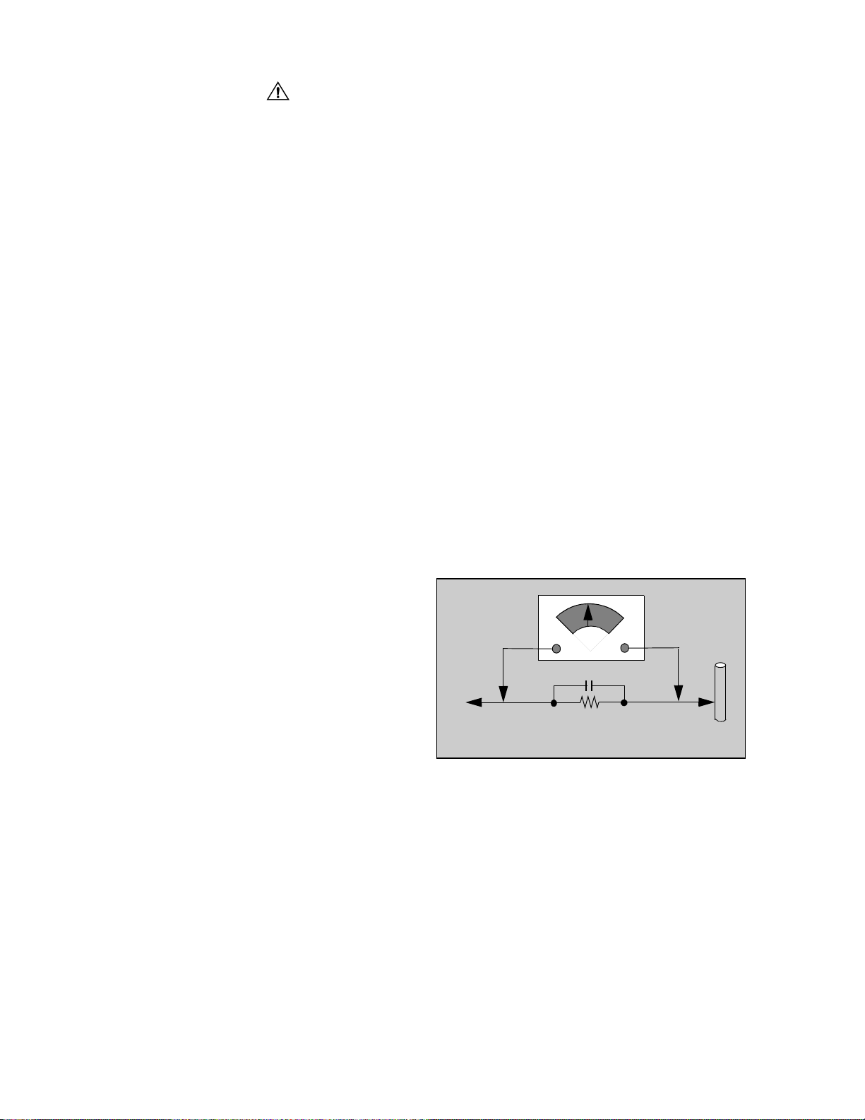
Leakage current hot check (Fig. 1)
Plug the AC cord directly into the AC outlet. Do not use
an isolation transformer during the check.
Connect a 1.5kΩ 10 watt resistor in parallel with a
0.15µF capacitor between an exposed metallic part
and ground. Use earth ground, for example a
water pipe.
Using a DVM with a 1000 ohms/volt sensitivity or
higher, measure the AC potential across the resistor.
Repeat the procedure and measure the voltage
present with all other exposed metallic parts.
Verify that any potential does not exceed 0.75 volt
RMS. A leakage current tester (such a Simpson model
229, Sencore model PR57 or equivalent) may be used
in the above procedure, in which case any current
measure must not exceed 0.5 milliamp. If any
measurement is out of the specified limits, there is a
possibility of a shock hazard and the receiver must be
repaired and rechecked before it is returned to the
customer.
AC VOLTMETER
COLD
WATER
PIPE
(GROUND)
0.15µF
TO
INSTRUMENT’S
EXPOSED METAL
PARTS
1500Ω,10 W
Figure 1. Hot check circuit
X-ray radiation
WARNING: The potential source of X-ray radiation in the
TV set are the High Voltagesection and the picture tube.
Refer to X-RAY protecton circuit check in service
notes in this manual to confirm HHS voltage.
High voltage (crt anode)
Confirm Anode voltage is within limits:
Set the BRIGHTNESS, PICTURE, SHARPNESS and
COLOR to minimum (To obtaina dark image). Measure
high voltage. It should be:
26.60
± 1.25kV.
If the upper limit is out of tolerance, immediate service
and correction is required.
Note: It is important to use an accurate, calibrated
high voltage meter.
-2-

Importantsafetynotice................... 2
Safetyprecautions................. 2
Generalguidelines................. 2
Leakage current cold check . . . . . . . . . . 2
Leakage current hot check . . . . . . . . . . . 2
X-rayradiation.................... 2
Highvoltage(crtanode)............. 2
Servicenotes........................... 4
Leadless chip component
(surfacemount)................ 4
Componentremoval................ 4
Chip component Installation . . . . . . . . . . 4
HowtoreplaceFlat-IC.............. 4
X-rayprotectioncircuitcheck......... 5
Receiverfeaturetable.................... 6
Chasis service adjustment procedures. . . . . . 7
130.0V B+ voltage confirmation . . . . . . . 7
Sourcevoltagechart................ 7
Highvoltagecheck................. 7
Audiosignalpathblockdiagram........... 8
Videosignalpathblockdiagram........... 9
Partslist.............................. 10
Foldouts, voltages & waveforms . . . . . . . 18~31
-3-
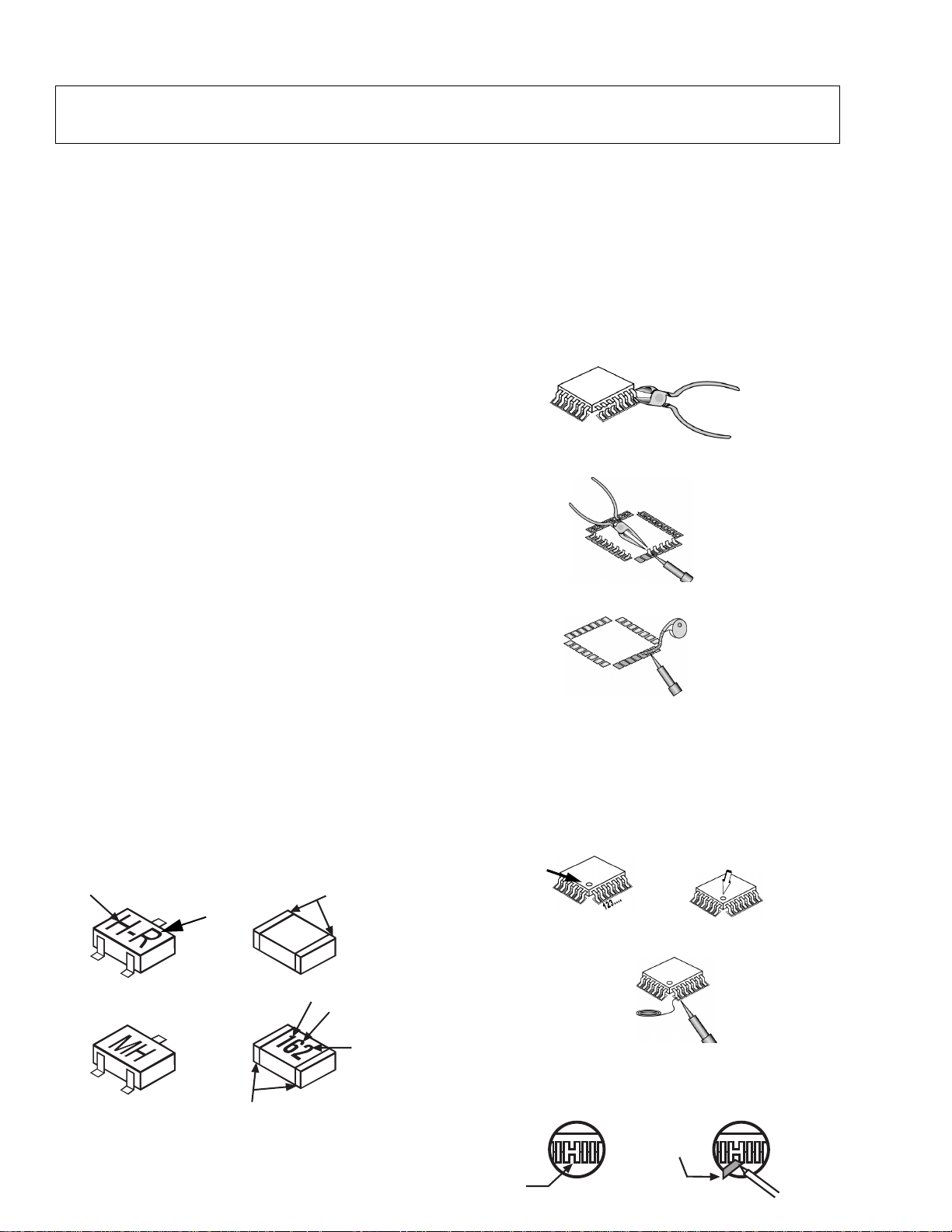
Service notes
Note: These components are affixed with glue. Be careful not to break or damage any foil under the
component or at the pins of the ICs when removing. Usually applying heat to the component for a short time
while twisting with tweezers will break the component loose.
Leadless chip component
(surface mount)
Chip components must be replaced with identical chips
due to critical foil track spacing. There are no holes in
the board to mount standard transistors or diodes.
Some chips capacitor or resistor board solder pads
may have holes through the board, however the hole
diameter limits standard resistor replacement to 1/8
watt. Standard capacitor may also be limited for the
same reason. It is recommended that identical
components be used.
Chip resistor have a three digit numerical resistance
code - 1st and 2nd significant digits and a multiplier.
Example: 162 = 1600 or 1.6kΩ resistor, 0 = 0Ω (jumper).
Chip capacitors generally do not have the value
indicated on the capacitor. The color of the component
indicates the general range of the capacitance.
Chip transistors are identified by a two letter code. The
first letter indicates the type and the second letter, the
grade of transistor.
Chip diodes have a two letter identification code as per
the code chart and are a dual diode pack with either
common anode or common cathode. Check the parts
list for correct diode number.
Component removal
1. Use solder wick to remove solder from component
end caps or terminal.
2. Without pulling up, carefully twist the component
with tweezers to break the adhesive.
3. Do not reuse removed leadless or chip
components since they are subject to stress
fracture during removal.
Chip component Installation
1. Put a small amount of solder on the board
soldering pads.
2. Hold the chip component against the soldering
pads with tweezers or with a miniature alligator clip
and apply heat to the pad area with a 30 watt iron
until solder flows. Do not apply heat for more than
3 seconds.
TYPE
b
e
ANODES
MH DIODE
Chip components
GRADE
c
TRANSISTOR
COMMON
CATHODE
SOLDER
CAPS
CAPACITOR
1ST DIGIT
RESISTOR
SOLDER
CAPS
2ND DIGIT
MULTIPLIER
=1600 = 1.6k
How to replace Flat-IC
- Required tools -
• Soldering iron • De-solder braids
• Sharpen pliers (wire
cutters and long nose)
1. Cut the pins ofthe defective IC with the wire cutters
pliers, and remove it completely away from the
board. If the IC is glued to the board, apply hot air
to complete the removal. CAUTION- Do not pull or
twist the pliers, may damage the soldering pads in
the board.
Flat-IC
2. Using the soldering Iron and the long nose pliers,
remove the IC pins that still attached to the board.
3. Using the de-solder braid and the soldering iron,
remove the solder from the board soldering pads.
4. Position the new Flat-IC in place (apply the pins of
the Flat-IC to the soldering pads where the pins
need to be soldered). Properly determine the
positions of the soldering pads and pins by
correctly aligning the polarity symbol. Start aligning
and soldering pin no.1, then align and solder the
pin in the apposite corner of the IC, this will help to
align the rest of the pins.
Polarity
symbol
5. Solder all pins to the soldering pads using a fine
tipped soldering iron.
Solder
6. Check with a magnifier for solder bridge between
the pins or for dry joint between pins and soldering
pads. To remove a solder bridge, use a de-solder
braid as shown in the figure below.
Solder
bridge
-4-
• Magnifier
Soldering
iron
De-Solder
braid
Soldering
iron
Soldering
iron
De-Solder
braid
Soldering
iron
Service notes (continued)
IMPORTANT: To protect against possible damage to
the solid state devices due to arcing or static discharge,
make certain that all ground wires and CTR DAG wire
are securely connected.
CAUTION: The power supply circuit is above earth
ground and the chassis cannot be polarized. Use an
isolation transformer when servicing the receiver to
avoid damage to the test equipment or to the chassis.
Connect the test equipment to the proper ground ( ) or
( ) when servicing, or incorrect voltages will be
measured.
Procedure:
1. Connect receiver to isolator transformer.
2. Apply a monoscope pattern.
3. In service mode. (Refer to service mode section)
select register C0b.
4. Measure TP5 (TPs port close to tuner). Compare
the measure of TP5 and set the data for C0b
according the following table
TP5
MEASURE (V)
DATA TO
C0b (Hex)
WARNING: This receiver has been designed to meet
or exceed applicable safety and x-ray radiation
protection as specified by government agencies and
independent testing laboratories.
To maintain original product safety design standards
relative to x-ray radiation and shock and fire hazard,
parts indicated with the symbol on the schematic
must be replaced with identical parts. Order parts from
the manufacturer’s parts center using the parts
numbers shown in this service manual, or provide the
chassis number and the part reference number.
For optimum performance and reliability, all other parts
should be replaced with components of
identical specification.
X-ray protection circuit check
This test must be performed as final check before the
receiver is returned to the customer. If voltage is out of
tolerance, immediate service and correction is required
to insure safe operation and to prevent the possibility of
premature component failure.
Equipment needed to check the protection circuit:
1. Isolator transformer.
2. High voltage meter.
3. Short jumper.
4. Diode connection jumper.
Use similar diode than D823, refer to parts list for
part No., (diode should support at least 150V.)
0 ~ 0.93 00
0.93 ~ 0.97 01
0.97 ~ 1.01 02
1.01 ~ 1.05 03
1.05 ~ 1.09 04
1.09 ~ 1.13 05
1.13 ~ 1.17 06
1.17 ~ 1.21 07
5. Exit service mode and turn receiver OFF.
6. Connect a jumper from TPD16 to TPD17.
7. Connect the
diode jumper
, cathode to TPD14
(cold GND), anode to TPD15 (hot GND).
Note: Refer to Fig. 2 for test point location.
8. Apply 75V AC to the AC input of the Insulator
transformer.Turn receiver ON.
9. Set PICTURE and BRIGTHNESS to minimum.
10. Increase the AC voltage at the input of Insulator
transformer and confirm the HHS voltage is
32.0kV, at the point set starts to loose sync,
11. Reset picture controls to original levels.
12. Turn the set OFF, and remove all jumpers and
connections from chassis.
-5-

Receiver feature table
FEATURE\MODEL CT-20G7DF CT-20D12DF
Chassis No AP391 BP391
Family NA7DM
Number of channels 181
Menu language Eng/Span/Fr
Closed Caption X
V-Chip X
75 Ω input X
Remote Model number EUR501450 EUR51 1502
Picturetubetype PANABLACK
Picture tube Supplier SAMSUNG
Comb Filter 2DIG
V/A norm V
FM Radio ---- X
MTS/SAP/DBX X
Built-in audio power 1.5Wx2 (10%)
Number of speakers 2
AI Sound X
A/V in (rear/front) 1(1/1)
Audio Out (F:FAO/V:VAO) --- F,V
S-VHS In (rear/front) --- 1/0
EPJ/HPJ/MISC HPJ
Dimensions mm
(WxDxH) in
Weight (kg/lbs) 18/39.6
Anode voltage
Video input jack 1Vp-p 75Ω, phono
Audio input jack 500mV rms, 47KΩ
A-Board TNP2AH040 DH* DK*
C-Board TNP2AA106 AF*
515.7x490.5x461.7
20.30x19.31x18.17
± 1.25 kV
26.60
Table 1. Receiver features
*Note: When ordering a board, add and ” S” after the board suffix application.
Example, If order A-Board for CT-20G7DF, should be ordered as:
TNP2AH040
DHS.
Specifications are subject to change without notice or obligation.
Dimensions and weights are approximate.
-6-
Chasis service adjustment procedures
All service adjustments are factory preset and should not require adjustment unless controls and/or
associated components are replaced.
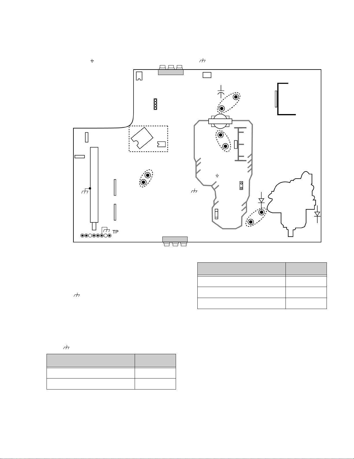
Note: Connect the (-) lead of the voltmeter to the appropriate ground. Use IC801’s heat sink when the HOT
ground symbol ( ) is used. Otherwise, use COLD ground ( ) — tuner shield, IC451’s heat sink or FA2.
Figure 2. A-Board main
components
and test points
IC552
IC551
T
U
N
E
R
FA1
CLK
DATA
FA2
IC2302
IC2301
IC002
IC001
A11
TPE10
TPE11
IC050
COLD ( )
IC003
C825
TPD17
TPD15
TPD16
HOT ( )
F801
IC801
TPD14
CRT
GND
TPD9
IC451
D561
TPD8
D554
SCREENFOCUS
COMPONENTS WITHIN DOT LINES ARE LOCATED AT THE OPOSITESIDE OF BOARD.
130.0V B+ voltage confirmation
1. Set the BRIGHT and the PICTURE to minimum by
using the PICTURE menu.
2. Connect the DVM between C825 (+ side) and cold
ground ( ).
3. Confirm that B+ voltage is 130.0V ± 2.5V.This
voltage supplies B+ to the horizontal output &
flyback circuits.
Source voltage chart
120V AC line input. Set the BRIGHT and the PICTURE
to minimum by using the PICTURE menu. Use cold
ground
(
) for the (-) lead of the DVM.
LOCATION VOLTAGE
TPD8 26.0V ± 2V
TPD9 25.0V ± 2V
LOCATION VOLTAGE
IC552 Pin3 5.0V ± 0.25V
IC551 Pin3 9.0V ± 0.25V
D554 Cathode 200V ± 15V
Adjust PICTURE menu for normalized video
adjustments.
High voltage check
1. Select an active TV channel and confirm that the
horizontal is in sync.
2. Adjust BRIGHTNESS and PICTURE using picture
icon menu, so video just disappears.
3. Confirm B+ 130V is within limit.
4. Using a high voltage meter confirm that the high
voltage is:
26.60kV±1.25kV
-7-
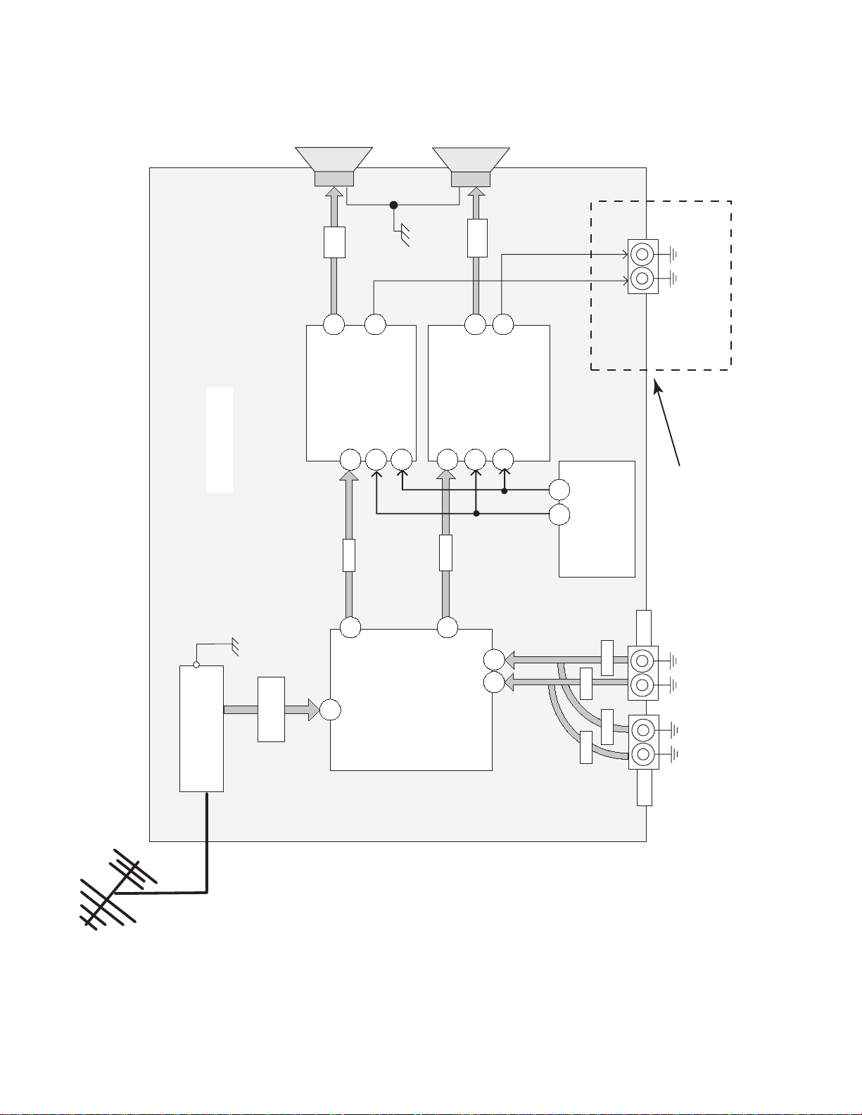
Audiosignalpathblockdiagram
A-BOARD
LEFT
SPEAKER
-
+
OUT
LEFT
5
10
OUT
VAO
LEFT
AUDIO AMP
LEFT CHANNEL
TV IN
3
LEFT
VOL
6
SP SW
RIGHT
TV IN
3
RIGHT
SPEAKER
-
+
OUT
RIGHT
10
OUT
RIGHT
VOL
699
5
VAO
AUDIO AMP
RIGHT CHANNEL
SP SW
JK3002
REAR A/V
OUT
AUDIO
67
SP / CP
64
VOL
IC001
MPU/VCJ
M65580MAP10
only for CT-20D12DF
TNR001
MAIN TUNER
MTS
22
OUT
RIGHT
IN
RIGHT
IN
LEFT
ANN5829S-E1V.
CHANNELS
LEFT&RIGHT
21
OUT
LEFT
14
MPX IN
IC2201
Figure 3. Audio signal block diagram
A/V 2
2 3
RIGHT RIGHT
LEFT LEFT
JK3002
REAR A/V
JK3001
A/V 1
FRONT A/V
-8-
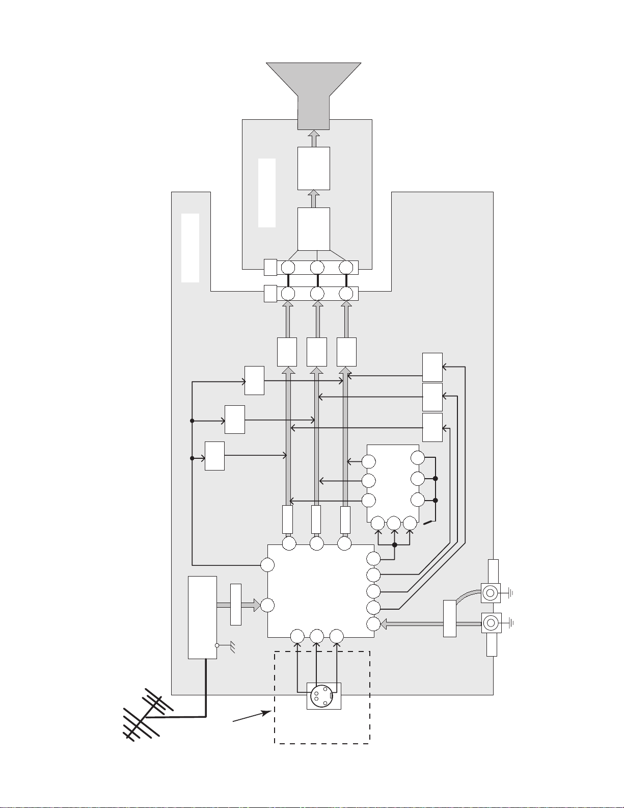
Videosignalpathblockdiagram
Q353 -B
Q351 -R
Q352 -G
C-BOARD
Q356 -B
Q354 -R
Q355 -G
1
2
A-BOARD
C1
A11
1
3
2
3
Q053
TNR001
MAIN TUNER
Q055
Q054
V IDEO IN
Q006
Q007
Q008
Q050 Q053 Q053
R
41 8
IC050
2 3 9
HALFTONE
6
TONE
HALF-
R
GB
OSD
EXT
5
59
48 49 51
20
R-OUT
G-OUT
B-OUT
28
28
FB
IC001
26
TV IN
Y IN
22
32
30
MPU/VCJ
M65580MAP10
C IN
SSW
24
72
13
3.3V
A/V 2
JK3002
REAR A/V
V IDEO IN
A/V 1
JK3001
FRONT A/V
JK3001
only for CT-20D12DF
Figure 4. Video signal block diagram
-9-

REPLACEMENT PARTS LIST
Models: CT-20D12DF, CT-20G7DF
Important Safety Notice: Components printed in BOLD TYPE have special characteristics important for safety. When replacing
any of these components use only manufacturer’s specified parts.
REF NO. PART NO. DESCRIPTION
CAPACITORS
C001 TCJ2VF1H103Z CAP,C .01UF-Z-50V
C002 TCJ2VB1H471K CAP,C 470PF-K-50V
C003 ECA1HM4R7B CAP,E 4.7UF-50V
C004 TCJ2VC1H150J CAP,C 15PF-J-50V
C005 TCJ2VC1H150J CAP,C 15PF-J-50V
C008 TCJ2VF1H104Z CAP,C .1UF-Z-50V
C009 ECA1AM470B CAP,E 47UF-10V
C010 TCJ2VF1H104Z CAP,C .1UF-Z-50V
C011 ECA1AM101B CAP,E 100UF-10V
C015 ECJ2VB1C224K CAP,C .22UF-K-16V
C016 TCJ2VC1H101J CAP,C 100PF-J-50V
C017 TCJ2VB1C104K CAP,C .1UF-K-16V
C018 TCJ2VC1H151J CAP,C 150PF-J-50V
C020 TCJ2VB1C104K CAP,C .1UF-K-16V
C022 TCJ2VC1H101J CAP,C 100PF-J-50V
C023 TCJ2VC1H151J CAP,C 150PF-J-50V
C024 ECA1AM470B CAP,E 47UF-10V
C025 TCJ2VB1C104K CAP,C .1UF-K-16V
C026 TCJ2VB1C104K CAP,C .1UF-K-16V
C027 TCJ2VC1H391J CAP,C 390PF-J-50V
C028 TCJ2VB1C104K CAP,C .1UF-K-16V
C029 ECQB1H333JF3 CAP,P .033UF-J-50V
C031 ECA1HMR22B CAP,E .22UF-50V
C032 ECA1AM470B CAP,E 47UF-10V
C033 TCJ2VC1H390J CAP,C 39PF-J-50V
C034 TCJ2VF1H103Z CAP,C .01UF-Z-50V
C035 ECA1HM010B CAP,E 1UF-50V
C036 TCJ2VF1H103Z CAP,C .01UF-Z-50V
C037 ECA1HM0R1B CAP,E 0.1UF/50V
C038 ECA1AM470B CAP,E 47UF-10V
C040 ECA1AM470B CAP,E 47UF-10V
C041 ECA1HM2R2B CAP,E 2.2UF-50V
C042 TCJ2VF1H104Z CAP,C .1UF-Z-50V
C043 ECA1AM470B CAP,E 47UF-10V
C044 TCJ2VC1H471J CAP,C 470PF-J-50V
C045 ECA1HM0R1B CAP,E 0.1UF/50V
C046 TCJ2VB1C104K CAP,C .1UF-K-16V
C047 TCJ2VC1H220J CAP,C 22PF-J-50V
C048 TCJ2VC1H220J CAP,C 22PF-J-50V
C050 ECA1AM101B CAP,E 100UF-10V
C051 TCJ2VF1H104Z CAP,C .1UF-Z-50V
C054 TCJ2VF1H103Z CAP,C .01UF-Z-50V
PARTS LIST
C055 TCJ2VC1H560J CAP,C 56PF-J-50V
C057 ECKR1H471KB5 CAP,C470PF-K-50V
C103 ECA0JM331B CAP,E 330UF-6.3V
C104 TCJ2VF1H103Z CAP,C .01UF-Z-50V
C105 ECA0JM101B CAP,E 100UF-6.3V
C350 ECA1CM101B CAP,E 100UF/16V
C351 TCJ2VB1H391K CAP,C 390PF-K-50V
C352 TCJ2VB1H391K CAP,C 390PF-K-50V
CT-20D12DF
CT-20D12DF
REF NO. PART NO. DESCRIPTION
C353 TCJ2VB1H471K CAP,C 470PF-K-50V
C354 ECKW3D102KBN CAP,C .001UF-K-2KVDC
C357 EEANA1E1R0B CAP,E 1.0U F- 25V
C361 TCJ2VC1H151J CAP,C 150PF-J-50V
C362 TCJ2VC1H151J CAP,C 150PF-J-50V
C363 TCJ2VC1H151J CAP,C 150PF-J-50V
C451 ECA1CHG470B CAP,E 47UF-16V
C452 ECSF1EE105VB CAP,E 1.0UF-25V
C453 ECEA1HFS2R2B CAP,E 2.2UF-50V
C454 ECA1EM102E CAP,E 1000UF-25V
C455 ECA1EHG101B CAP,E 100UF -25V
C456 ECQB1H103JF3 CAP,P .01UF-J-50V
C459 ECA1VHG471B CAP,E 470UF -35V
C462 ECA1HM4R7B CAP,E 4.7UF-50V
C502 TCJ2VC1H471J CAP,C 470PF-J-50V
C503 TCJ2VB1C104K CAP,C.1UF-K-16V
C504 TCJ2VB1C104K CAP,C .1UF-K-16V
C510 ECCR2H100D5 CAP,C 10PF-D-500V
C511 ECKR2H821KB5 CAP,C 820PF-K-500V
C512 ECKR2H101KB5 CAP,C 100UF-K-500V
C531 ECA1EM220B CAP,E 22UF-25V
C551 ECA1VM331B CAP,E 330UF-35V
C554 ECKR2H561KB5 CAP,C 560PF-K-500V
C555 ECA2EM220E CAP,E 22UF-250V
C556 ECA1CM471B CAP,E 470UF-16V
C557 ECKR2H222KB5 CAP,C 2200PF-K-500V
C560 ECEA1HN010UB CAP,E 1UF/50V
C561 ECKR2H561KB5 CAP,C 560PF-K-500V
C563 ECWH12H362JS CAP,P 3600PF-J-1250 VDC
C564 ECWH12H562JS CAP,P .0056UF-J-1.2KV
C565 ECKW3D331JBR CAP,C 330PF-J-2KV
C566 ECKW3D181JBP CAP,C 180PF-J-2KV
C568 ECQM4473JZW CAP,P .047UF-J-400V
C569 ECWF2394JBB CAP,P .39UF-J-200V
C570 ECA1CM222E CAP,E 2200UF-16V
C571 ECA1EM220B CAP,E 22UF-25V
C572 ECA1CM100B CAP,E 10UF-16V
C573 ECA1CM101B CA P,E 100UF/16V
C575 ECA0JM222B CAP,E 2200UF-6.3V
C577 ECA1CM101B CA P,E 100UF/16V
C578 ECA0JM332B CAP,E 3300PF-6.3V
C579 TCJ2VC1H100D CAP,C 10PF-J-50V
C580 ECKR2H152KB5 CAP,C .0015UF-K-500V
C605 TCJ2VF1H103Z CAP,C .01UF-Z-50V
C606 ECA0JM221B CAP,E 220UF-6.3V
C800 ECKR3A391KBP CAP,C 390PF-K-1KVDC
C801 ECKWAE472ZED CAP,C4700PF-Z-500V
C802 ECKWAE472ZED CAP,C 4700PF-Z-500V
C803 ECKWAE472ZED CAP,C4700PF-Z-500V
C805 EC0S2DA221BB CAP,E 220UF/200V
C806 ECQM4103KZW CAP,P .01UF-K-400V
Parts List
-10-
120-02

REPLACEMENT PARTS LIST
Models: CT-20D12DF, CT-20G7DF
Important Safety Notice: Components printed in BOLD TYPE have special characteristics important for safety. When replacing
any of these components use only manufacturer’s specified parts.
REF NO. PART NO. DESCRIPTION
C807 ECKR3A821KBP CAP,C 820PF-K-1KV
C808 ECA1VM101B CAP,E 100UF-35V
C809 ECKR1H101KB5 CAP,C100PF-K-50V
C810 ECKR1H471KB5 CAP,C470PF-K-50V
C812 ECQU2A224MVA CAP,P .22UF-M-250VAC
C813 ECQU2A153MVA CAP,P .015UF-M-250VAC
C814 ECQU2A153MVA CAP,P .015UF-M-250VAC
C820 ECA1CM101B CAP,E 100UF/16V
C821 TCJ2VF1H103Z CAP,C .01UF-Z-50V
C822 ECKR3A221KBP CAP,C 220PF-K-1KV
C823 ECA1VM471E CAP,E 470UF-35V
C824 ECKR3A102KBP CAP,C 1000PF-K-1KV
C825 EEUMG2C221S CAP,E 220UF-160V
C826 ECKR3A471KBP CAP,C 470PF-K-1KV
C827 ECA1CM471B CAP,E 470UF-16V
C828 ECA160V33UE CAP,E 33UF/160V
C2201 ECA1HM4R7B CAP,E 4.7UF-50V
C2202 ECA1HM2R2B CAP,E 2.2UF-50V
C2203 ECA1HM4R7B CAP,E 4.7UF-50V
C2204 AP106K016CAE CAP,T 10UF/16V
C2205 ECA 1HMR33B CAP,E .33UF-50V
C2206 ECQB1H223JF3 CAP,P .022UF-J-50V
C2207 AP335K016CAE CAP,T 3.3UF/16V
C2208 TCJ2VB1C104K CAP,C .1UF-K-16V
C2209 TCJ2VB1C104K CAP,C .1UF-K-16V
C2210 TCJ2VB1C104K CAP,C .1UF-K-16V
C2212 ECQB1H473JF3 CAP,P .047U F-J-50V
C2213 ECA1HMR47B CAP,E .47UF-50V
C2214 ECA1AM101B CAP,E 100UF-10V
C2215 EEANA1E100B CAP,E 10UF-25V
C2216 TCJ2VC1H100D CAP,C 10PF-J-50V
C2301 ECA1EM102E CAP,E 1000UF-25V
C2302 ECEA1HN010UB CAP,E 1UF/50V
C2303 ECA1EM101B CAP,E 100UF-25V
C2304 ECA1CM100B CAP,E10UF-16V
C2307 ECA1CM102B CAP,E1000UF/16V
C2309 ECA1HM010B CAP,E 1UF-50V
C2311 ECA1EM102E CAP,E 1000UF-25V
C2312 ECEA1HN010UB CAP,E 1UF/50V
C2313 ECA1EM101B CAP,E 100UF-25V
C2314 ECA1CM100B CAP,E10UF-16V
C2317 ECA1CM102B CAP,E1000UF/16V
C2319 ECA1HM010B CAP,E 1UF-50V
C2320 ECA1CM100B CAP,E10UF-16V
C2330 ECA1CM100B CAP,E10UF-16V
C2350 ECA1HM100B CAP,E10UF/50V
C3001 ECA1HM0R1B CAP,E 0.1UF/50V
C3012 ECA1HM010B CAP,E1UF-50V
C3018 ECA1HM010B CAP,E 1UF-50V
C3050 TCJ2VF1H103Z CAP,C.01UF-Z-50V
C3051 TCJ2VF1H103Z CAP,C.01UF-Z-50V
CT-20D12DF
CT-20D12DF
CT-20D12DF
CT-20D12DF
REF NO. PART NO. DESCRIPTION
DIODES
D002 MA165TA5VT DIODE, SWITCHING
D006 MA4330HTA DIODE
D052 MA4068MTA DIODE, ZENER
D053 MA4056MTA DIODE
D055 MA4056MTA DIODE
D451 ERA15-01V3 DIODE, RECTIFIER
D452 MA4047MTA DIODE
D453 MA165TA5VT DIODE, SWITCHING
D454 MA165TA5VT DIODE, SWITCHING
D456 MA4047MTA DIODE
D502 MA4047MTA DIODE
D531 AS01V0 DIODE
D551 D1NL20UV70 DIODE
D554 AU02V0 DIODE
D558 RS3FS DIODE
D559 BYD33G-113 DIODE
D561 AU02V0 DIODE
D571 MA165TA5VT DIODE, SWITCHING
D606 MA165TA5VT DIODE, SWITCHING
D607 MA152KTX DIODE
D608 MA152KTX DIODE
D609 MA152KTX DIODE
D801 D3SBA60-4103 DIODE
D806 TAP2AA0001 PTC 5-OHM
D808 SARS01V1 DIODE
D809 AG01V0 DIODE
D810 AG01V0 DIODE
D811 AG01V0 DIODE
D812 MA4068MTA DIODE, ZENER
D820 MA165TA5VT DIODE, SWITCHING
D821 MA4047HTA DIODE
D822 RN1ZLF-B1 DIODE
D823 S3L60P154004 DIODE
D824 D1NL20UV70 DIODE
D2305 MA3110MTX DIODE, ZENER
D2306 MA3110MTX DIOD E, ZENER
D2307 MA3110MTX DIODE, ZENER
D2308 MA3110MTX DIOD E, ZENER
D2350 MA4068MTA DIODE, ZENER
D2351 MA165TA5VT DIODE, SWITCHING
D2352 MA165TA5VT DIODE, SWITCHING
D2353 MA165TA5VT DIODE, SWITCHING
D2354 MA4091MTA DIODE
D3001 MA3110MTX DIOD E, ZENER
D3003 MA3110MTX DIODE, ZENER
D3004 MA3110MTX DIOD E, ZENER
D3005 MA3110MTX DIODE, ZENER
D3006 MA3110MTX DIOD E, ZENER
D3017 MA3110MTX DIODE, ZENER
D3018 MA3110MTX DIOD E, ZENER
CT-20D12DF
CT-20D12DF
CT-20D12DF
CT-20D12DF
PARTS LIST
120-02
-11-
Parts List
 Loading...