

Page 1
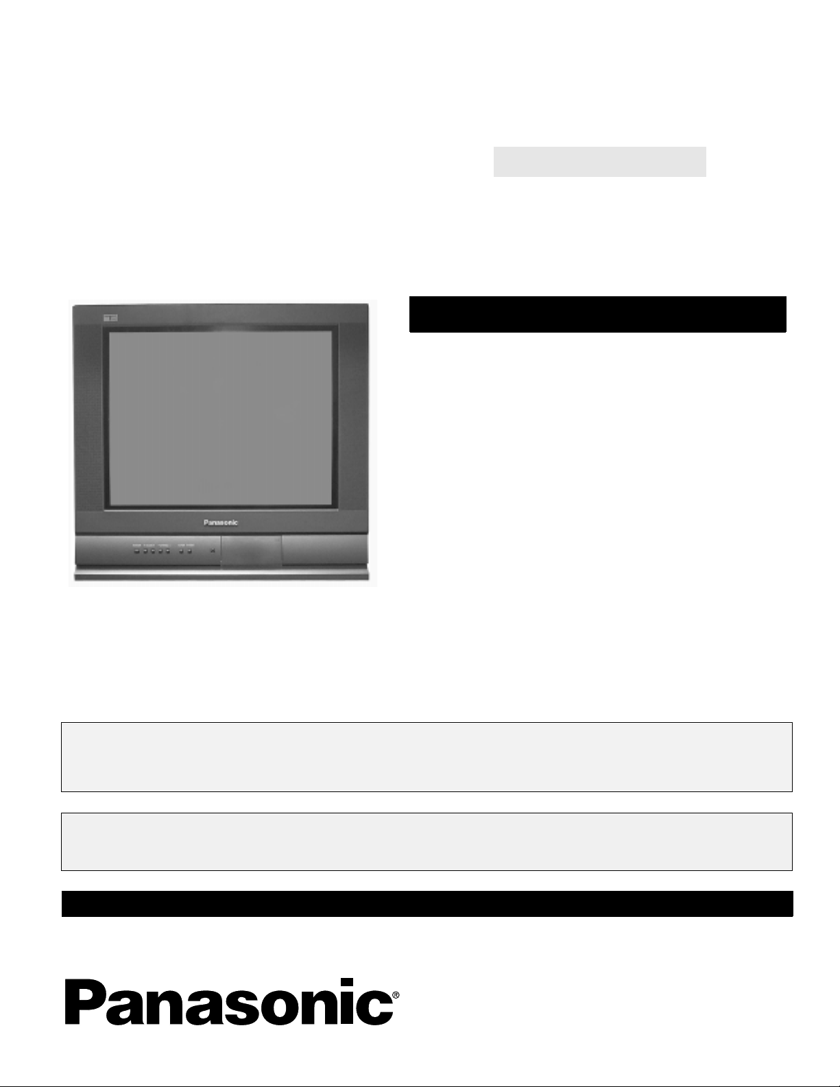
ORDER NO. MTNC010735C1
B1
Service Manual
Color Television
Main Manual
(NA6DV)
Panasonic
Models
Chassis
CT-20SX11E AP380
CT-20SX11CE AP380
This Service man ual is issued as a service guide for the models o f the NA6DV fam ily listed abov e. Included in th is
manual are a set of schematics, block diagrams, functional descriptions, alignment procedures, disassembly
procedures, and a complete parts list.
“WARNING! This Service Man ual is desig ned for expe rienced repa ir technici ans only and is not designed f or use by t he general p ublic.
It does not contain warnings or cautions to advise non-technical individuals of potential dangers in attempting to service a product.
Products powered by electricity should be serviced or repaired only by experien ced profess ional techn icians. Any attempt to
service or repair the product or products dealt with in this Service Manual by anyone else could result in serious injury or death.”
The service technician is required to read and follow the “Safety Precautions” and “Important Safety Notice” in this Main Manual.
Copyright 2001 by Matsushita Electric Corporat ion of
America. All rights reserved. Unauthorized copying
and distribution is a violation of law.
Page 2
Important Safety Notice
Special components are used in this television set which are important for safety. These parts are identified on the
schematic diag ram by the s ymbol and printed in BOLD TYPE o n the replac ement part l ist. It is es senti al that
these critical parts are replaced with the manufacturer ’s specified replacement part to prevent X-ray radiation,
shock, fire or other hazards. Do not modify the original design without the manufacturer’s permission.
Safety Precautions
General Guidelines
An Isolation Transformer should always be used
during the servicing of a r eceiver whose c hassis is not
isolated from AC power line. Use a transformer of
adequate power rating as this protects the technician
from accidents resulting in personal injury from
electrical shocks. It will also protec t the Receiver from
being damaged by accidenta l shorting that may occur
during servicing.
When servicing, observe the original lead dress,
especially in the high voltage circuit. Replace all
damaged parts (also parts that show signs of
overheating.)
Always Replace Protective Devices, such as
fishpaper, isolation resistors and capacitors, and
shields after servicing the Receiver. Use only
manufacturer ’s recommended rating for fuses, c ircuits
breakers, etc.
High potentials are present when this Receiver is
operating. Operation of the Receiver without the rear
cover introduces danger for elect rical shock. S ervicing
should not be performed by anyone who is not
thoroughly familiar with the necessary precautions
when servicing high-voltage equipment.
Extreme care should be practiced when Handling the
Picture T ube. Rough handling may cause it to implode
due to atmospheric pres sure. (14.7 lbs per sq. in.). D o
not nick or scratch the glass or subject it to any undu e
pressure. When handling, use safety goggles and
heavy gloves for protection. Discharge the picture
tube by shorting the anode to chassis ground (not to
the cabinet or to other mounting hardware). When
discharging con nec t co ld ground (i.e. da g gr oun d lea d)
to the anode with a well insulated wire or use a
grounding probe.
Avoid prolonged exposure at close range to unshielded
areas of the picture tube to prevent exposure to Xray radiation.
The Test Picture Tube used for servicin g the chassis
at the bench should incorporate safety glass and
magnetic shieldi ng. The safety glass pro vide shielding
for the tube viewing area against X-ray radiation as
well as implosion. The magnetic sh ield limits the X-ray
radiation around the bell of the pict ure tube in addition
to the restricting magnetic effects. When using a
picture tube test jig for service, ensure that the jig is
capable of handling 40kV without causing Xray radiation.
Before returning a serviced rec eiver to the owner,
the service technic ian must thoroughly test the unit to
ensure that is completely safe to operate. Do not use a
line isolation transformer when testing.
Leakage Current Cold Check
Unplug the AC cord and connect a jumper between the
two plug prongs.
Measure the resistance between the jumpered AC plug
and expose metallic parts such as screwheads,
antenna terminals, control shafts, etc. If the exposed
metallic part has a return path to the chassis, the
reading should be between 240kΩ and 5.2MΩ. If the
exposed metallic part does not have a return path to
the chassis, the reading should be infinite.
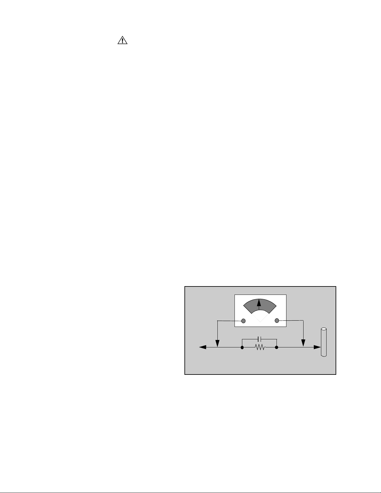
Leakage Current Hot Check (Fig. 1)
Plug the AC cord directly into the AC outlet. Do not use
an isolation transformer during the check.
Connect a 1.5kΩ 10 watt resistor in parallel with a
0.15µF capacitor between an exposed metallic part
and ground. Use earth ground, for example a
water pipe.
Using a DVM with a 1000 ohms/volt sensitivity or
higher, measure the AC potential across the resistor.
Repeat the procedure and measure the voltage
present with all other exposed metallic parts.
Verify that any potential does not exceed 0.75 volt
RMS. A leakage curr ent tes ter (suc h a S impson M odel
229, Sencore Model P R57 or equiv alent) may be used
in the above procedure, in which case any current
measure must not exceed 1/2 milliamp. If any
measurement is out of the specified limits, there is a
possibility of a s hock haz ar d and th e R ece iv er m us t b e
repaired and rechecked before it is returned to the
customer.
AC VOLTMETER
COLD
WATER
PIPE
(GROUND)
0.15µF
TO INSTRUMENT’S
EXPOSED METAL
PARTS
1500Ω,10 W
Figure 1. Hot Check Circuit
X-ray Radiation
WARNING: The potential source of X-ray radiation in the
TV set is in the H igh Voltage section and th e p ict ure tu be.
Note: It is important to use an accurate, calibrated
high voltage meter.
Set the brightness, picture, sharpness and color
controls to Minimum. Measure the High Voltage. The
high voltage should be 27.7kV ± 1.25kV. If the upper
limit is out of tolerance, immediate service and
correction is required to insure safe operation and to
prevent the possibility of premature component failure.
- 2 -
Page 3
Important Safety Notice . . . . . . . . . . . . . . . . . . 2
Safety Precautions. . . . . . . . . . . . . . . . . 2
Service Notes. . . . . . . . . . . . . . . . . . . . . . . . . . . 4
Receivers Feature Table. . . . . . . . . . . . . . . . . . 6
Location of Controls (Receiver)
Receiver Front Control Panel. . . . . . . . . 7
Location of Controls (Remote)
EUR511502 . . . . . . . . . . . . . . . . . . . . . . 8
Disassembly for Service. . . . . . . . . . . . . . . . . . 9
Disassembly for CRT Replacement. . . . . . . . . 9
Chassis Service Adjustment Procedures. . . 10
Service Adjustments
(Electronic Control). . . . . . . . . . . . . . . . . . 21
Sub-Brightness. . . . . . . . . . . . . . . . . . . 21
Video Adjustment Level . . . . . . . . . . . . 21
Sub-Contrast. . . . . . . . . . . . . . . . . . . . . 21
Tint/Color Adjustment. . . . . . . . . . . . . . 21
Color Temperature Adjustment. . . . . . . 22
Complete Adjustment. . . . . . . . . . . . . . 22
Horizontal Centering. . . . . . . . . . . . . . . 23
Audio Adjustment . . . . . . . . . . . . . . . . . 23
MTS Circuit Adjustment . . . . . . . . . . . . 23
Input Level Adjustment. . . . . . . . . . . . . 23
Stereo Separation Adjustment (Sb) . . . 23
Clock Adjustment (Sb) . . . . . . . . . . . . . 24
Vertical Size . . . . . . . . . . . . . . . . . . . . . 24
Service Adjustments
(Mechanical Controls). . . . . . . . . . . . . . . . 24
VCO Field Adjustment L105. . . . . . . . . 24
Focus (Part of T551). . . . . . . . . . . . . . . 24
E-W Pincushion . . . . . . . . . . . . . . . . . . 24
H-Width. . . . . . . . . . . . . . . . . . . . . . . . . 24
132V B+ Voltage Confirmation. . . . . . . 10
Source Voltage Chart. . . . . . . . . . . . . . 10
High Voltage Check . . . . . . . . . . . . . . . 10
Purity and Convergence Procedures . . . . . . .11
Service Mode (Electronic Controls). . . . . . . . 14
Entering Service Mode. . . . . . . . . . . . . 14
Toggle between Modes. . . . . . . . . . . . . 14
Exiting the Service Mode . . . . . . . . . . . 14
Sub-Data Adjustment. . . . . . . . . . . . . . 15
Cut-Off Adjustment. . . . . . . . . . . . . . . . 15
Options Adjustment . . . . . . . . . . . . . . . 16
MTS Adjustment. . . . . . . . . . . . . . . . . . 16
Comb Filter Adjustment . . . . . . . . . . . . 17
To Check Purity . . . . . . . . . . . . . . . . . . 18
Helpful Hints. . . . . . . . . . . . . . . . . . . . . 18
Instructional Flow Chart
for Service Mode. . . . . . . . . . . . . . . . . . . . 19
Audio Signal Path Block Diagram . . . . . . . . . 25
Video-Chroma Signal Path
Block Diagrams. . . . . . . . . . . . . . . . . . . . . 26
Component Identification. . . . . . . . . . . . . . . . 27
Parts List . . . . . . . . . . . . . . . . . . . . . . . . . . . . . 31
C-Board
Schematic, Layout & Voltages . . . . . . . . . . 38
A-Board Schematic
Left Section . . . . . . . . . . . . . . . . . . . . . . . . 39
Right Section. . . . . . . . . . . . . . . . . . . . . . . 40
A-Board Layout. . . . . . . . . . . . . . . . . . . . . . . 41
A-Board Voltages . . . . . . . . . . . . . . . . . . . . . 42
Z-Board
Schematic, Layout & Voltages. . . . . . . . . . 43
Waveforms
A-Board. . . . . . . . . . . . . . . . . . . . . . . . . . 44
- 3 -
Page 4
Service Notes
Chip Components
TRANSISTOR
CAPACITOR
RESISTOR
MH DIODE
SOLDER
CAPS
SOLDER
CAPS
1ST DIGIT
2ND DIGIT
MULTIPLIER
=1600 = 1.6k
GRADE
TYPE
COMMON
ANODES
CATHODE
Note: These components are affixed with glue. Be careful not to break or damage any foil under the
component or at the pins of the ICs when removing. Usually applying heat to the component for a
short time while twisting with tweezers will break the component loose.
Leadless Chip Component
(surface mount)
Chip components must be replaced with identical chips
due to critical foil tr ack spacing. There are no ho les in
the board to mount standard transistors or diodes.
Some chips capacitor or resistor board solder pads
may have holes thr ough the board, however the hole
diameter limits standard resistor replacement to 1/8
watt. Standard capacitor may also be limited for the
same reason. It is recommended that identical
components be used.
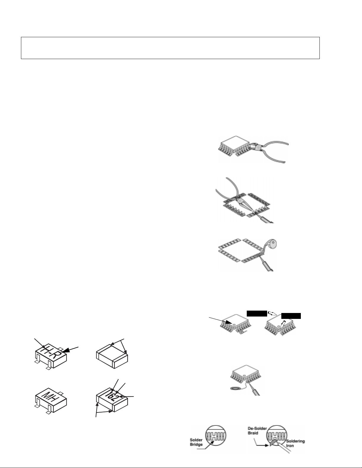
Chip resistor have a three digit numerical resistance
code - 1st and 2nd significant digits and a multiplier.
Example: 162 = 1600 or 1.6kΩ resistor, 0 = 0Ω (jumper).
Chip capacitors generally do not have the value
indicated on the capacitor. The color of the compo nent
indicates the general range of th e capacitance.
Chip transistors are id enti fied by a two letter c ode . Th e
first letter indicates the type and the second l etter, the
grade of transistor.
Chip diodes have a two lette r i den tif ic ati on code as per
the code chart an d are a dual diode pack with either
common anode or common cathode. Check the parts
list for correct diode number.
Component Removal
1. Use solder wick to remove s older fr om compo nent
end caps or terminal.
2. Without pulling up, carefully twist the component
with tweezers to break the adhesive.
3. Do not reuse removed leadless or chip
components since they are subject to stress
fracture during removal.
Chip Component Installation
1. Put a small amount of solder on the board
soldering pads.
2. Hold the chip component against the soldering
pads with tweezers or with a miniature alligator clip
and apply heat to the pad area with a 30 watt iron
until solder flows. Do not appl y heat for more than
3 seconds.
How to Replace Flat-IC
- Required Tools -
• Soldering iron • De-solder braids
• Needle nose pliers • Magnifier
• Wire cutters (sharp & small)
1. Cut the pins of a defective IC with wire cutters.
Remove IC from boar d. If IC i s glued to the boa rd,
heat the IC and release the IC. See Note above.
Flat IC
2. Using soldering iron and needle nose pliers
remove the IC pins from the board.
Soldering
Iron
3. Using de-soldering braid and soldering iron remove
solder from affected are on board (pads).
De-soldering
Braid
Soldering
Iron
4. Position the new Flat-IC in pl ace (apply the pins of
the Flat-IC to the soldering pads where the pins
need to be soldered). Determine the positions of
the soldering pads and pins by correctly aligning
the polarity symbol. Solder pin #1 first, align the IC.
Polarity
symbol
2nd solder
1st solder
b
e
c
Solder the pin op posite to pin #1. This will assist
positioning the IC.
5. Solder all pins to the soldering pads using a fine
tipped soldering iron.
Solder
Soldering
Iron
6. Check with a magnifier fo r solder bridge between
the pins or for d r y jo int b etwe en pi ns a nd so ld erin g
pads. To rem ove a solder bridge, use a de-solder
braid as shown in the figure below.
- 4 -
Page 5

Service Notes (Continued)
IMPORTANT: To protect against possible damage to
the solid state devices due to arcing or static
discharge, make cer tain that all g round wir es and CTR
DAG wire are securely connected.
WARNING: This Receiver has been designed to mee t
or exceed applicable safety and X-ray radiation
protection as specified by government agencies and
independent testing laboratories.
CAUTION: The power supply circuit is above earth
ground and the chassis cannot be polarized. Use an
isolation transformer when servicing the Receiver to
avoid damage to the test equipmen t or to the chassis.
Connect the test equipment to the proper ground ( ) or
( ) when servicing, or incorrect voltages will be
measured.
To maintain original product safety design standards
relative to X-ray radiation and shock and fire hazard,
parts indicated with the symbol on the schematic
must be replaced with identi cal parts. Order parts from
the manufacturer’s parts center using the parts
numbers shown in t his service manual, o r provide the
chassis number and the part reference number.
For optimum performanc e and rel iability, all other parts
should be replaced with components of
identical specification.
- 5 -
Page 6
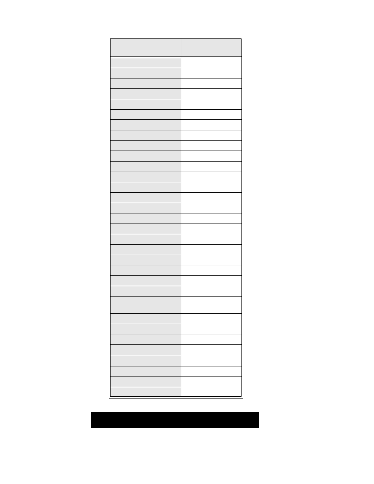
Receiver Feature Table
FEATURE\MODEL
Chassis AP380
Tuning system 40K
# of channels 181
Menu language Eng/Span/Fr
Closed Caption X
V-Chip X
75 Ω input X
Remote Model # EUR511502
Picture tube A51LSK955X-A
PureFlat Picture Tube X
Comb Filter 3 Line Digital
H. Edge Correction X
V/A norm Both
MTS/SAP/DBX X
Bass/Treble/Balance X
Surround Sound X
AI Sound X
CT-20SX11E &
CT-20SX11CE
FAO & VAO X
Built-in audio power 5Wx2 (10%)
# of speakers 2
A/V in (rear/front) 2(2/1)
S-VHS Input (rear/front) 1/0
Headphone Jack X
Dimensions mm
(WxDxH) in
Weight (kg/lbs) 24.5/54.13
Power source (V/Hz) 120/60
Anode voltage 27.7kV ± 1.25kV
Video input jack
Audio input jack 500mV RMS 47kΩ
A-Board TNP2AH019 KA
C-Board TNP2AA047 AY
Z-Board TNP2AA010 AJ
550x479x491.5
21.7 x 18.9 x 19.4
75Ω, phono jack
1V
p-p
Table 1. Receiver Features
Specifications are subject to change without notice or obligation.
Dimensions and weights are approximate.
- 6 -
Page 7
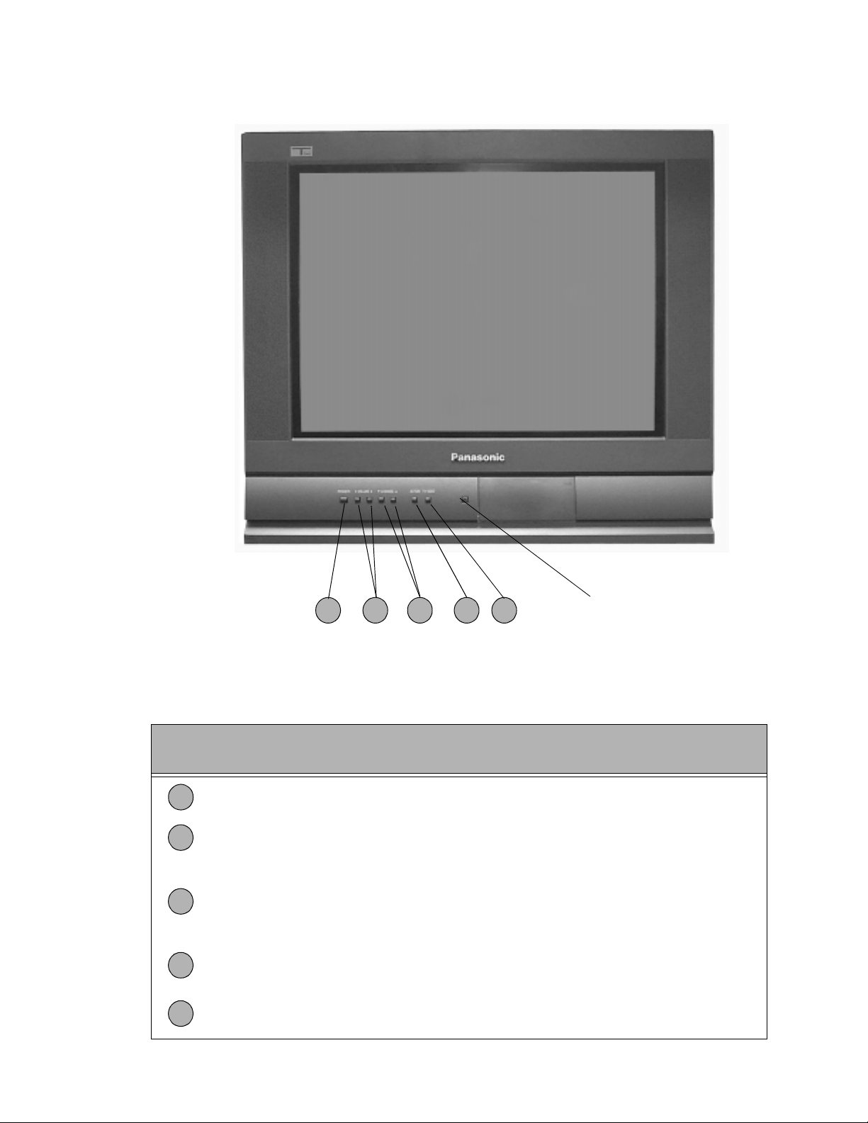
Location of Controls (Receiver)
1
4 532
Remote Control
Sensor
Figure 2. Location of Controls (Receiver).
Quick Reference Control Operation
Quick Reference
Control Operation
1
Power Button - Press to turn ON or OFF.
Volume Buttons - Press to adjust Sound Level, or to adjust Audio Menus, Video
2
Menus, and select operating features when menus are displayed
Channel Buttons - Press to sele ct programme d channels. Pre ss to highlight d esired
features when menus are dis play ed. Also us e to selec t Cable Conv erte r box chan nels
3
after programming Remo te Control Infra-red codes ( the TV/AUX/CABLE switc h must
be set in CABLE position).
Action Button - Press to display Main Menu and access On Screen feature and
4
Adjustment Menus.
5
TV/Video Button - Press to select TV or Video Input.
- 7 -
Page 8
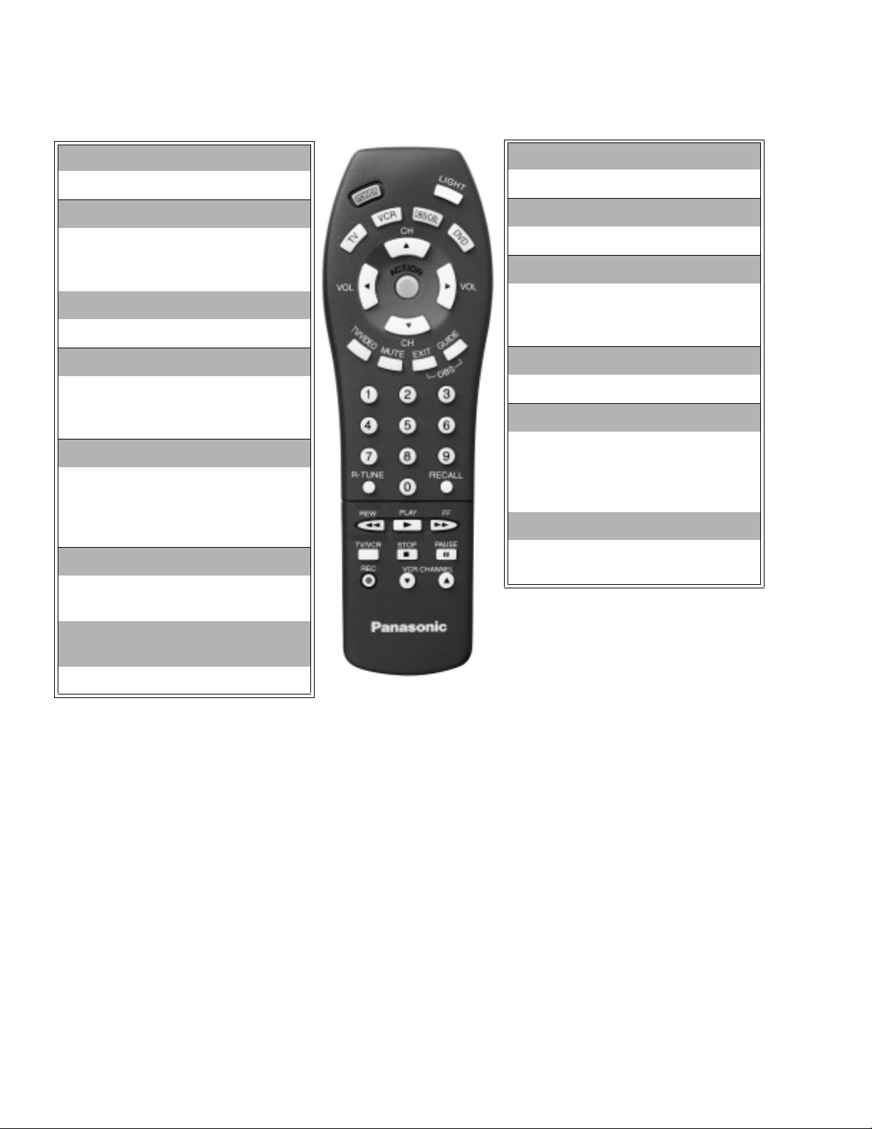
Location of Controls (Remote )
Power Button
Press to turn ON and OFF.
ACTION Button
Press to display Main Menu and
access or exit On Screen features
and Adjustment Menus.
TV, VCR, DBS/CBL, DVD
Component function buttons.
VOL (volume) Buttons
Press to adjust TV sound level.
Use with Channel buttons to
navigate in menus.
Mute Button
Press to mute sound.
A second press resumes sound.
Press also to access and delete
Closed Caption display.
R-TUNE (Rapid Tune) Button
Press to switch to the previous
channel.
LIGHT Butt o n
Press to light remote control buttons.
TV/VIDEO Button
Press to select TV or Video input.
CH (channel) Buttons
Press to select channels.
Use with volume buttons to
navigate in menus.
DBS EXIT, DBS GUIDE
DBS function buttons.
RECALL Button
Press to display Time, status
of Sleep Timer, Channel,
Video mode and Channel
Caption (Station Identifier).
“0” - “9”
Press numeric keypad to select any
channel.
REW, PLAY, FF, TV/VCR, STOP,
PAUSE, REC, VCR/DBS CH
Component function buttons.
Figure 3. Location of Controls (Remote).
EUR511502
- 8 -
Page 9

Disassembly for Service
Back Cover
Remove all the screws marked with an arrow( )
from the back of the Receiver.
Note: Screw configuration, type, and number of
screws vary depending on the model of the
Receiver serviced and the app lication; various
models are covered in this Manual. Us e same
hardware when reassembling the receiver.
• 2 screws at the top edge of the Receiver.
• 1 screw at each lower corner of the Receiver.
• 1 screw by the A/V jacks.
• 1 screw by the Fly-back assembly.
A-Board - Main Chassis
1. Slide the chassis completely out of the guide rails.
2. Stand the Receiver on its edge. The underside o f
the board is completely accessible for component
replacement.
Note: Some tie-wraps t hat secure the wire d ressings
may need to be unfastened for chassis
removal.
C-Board - CRT Output
Plugs into the socket on the CRT neck.
Z-Board - Pincushion Correction
Plugs into the A-Board.
Speakers
Speaker are secured to the s peak er brac ket with 4
screws, the bracket is secured to the cabinet’s front
with 2 screws.
Keyboard Push Button Assembly
Fastened to the inside of the cabinet front with up
to 3 screws.
Disassembly for CRT Replacement
1. Discharge the CRT as instructed in the Safety
Precautions (see page 2).
2. Disconnect the yoke (DY) plug, degaussing coil
(DEG) plug and the CRT 2nd anode button from
the main board.
3. Remove the C-Board from the CRT base and
unplug the black wire (CRT dag ground) C10.
4. Disconnect the A11, A12, and Speakers plugs from
the A-Board.
5. Lift the Main Chassis (A-Board) and all mounted
boards completely out with the CRT Board attached.
CRT Replacement
1. Perform Disassembly for CRT Replacement
procedure.
2. Insure that the CRT H.V. Anode button is
discharged before handling the CRT. Read the
Safety Precautions (see page 2) on handling the
picture tube.
3. Remove the components from the CRT neck and
place the cabinet face down on a soft pad.
4. Note the original order for the CRT mounting
hardware as they are remove from the CRT
mounting brackets at each corner of the CRT.
5. Remove the CRT with the dega ussing co il and th e
dag ground braid attached.
6. Note the original locations and mounting of the
degaussing coil and the dag ground assembly to
insure proper reinstallation on the replacement
CRT.
To remove and re-mount the degaussing coil:
The degaussing co il is held in place by clampers
fastened to the CRT corner ears. These c lampers
must be installed onto th e replacement CRT prior
to mounting the degaussing coil.
To remove and re-mount the dag ground braid:
a.Unhook the coil sprin g from the bottom corners
of the CRT ears.
b.Release the braid loop from the upper corners of
the CRT ears.
7. Mount the dag ground braid on the replacement
CRT. Position the degaussing coil with new ties.
Dress coil as was on the original CRT.
8. Replace the components on CRT neck and
reinstall into cabinet. Verify that all ground wires
and circuit board plugs get connected.
- 9 -
Page 10
Chassis Service Adjustment Procedures
All service adjustments are factory preset and should not require adjustment unless controls and/or
associated components are replaced.
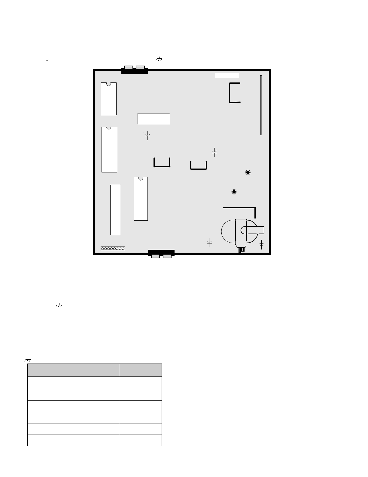
Note: Connect the (-) lead of the voltmeter to the appropriate ground. Use IC803’ s heat sink when the HOT ground
symbol ( ) is used. Otherwise, use COLD ground ( ) — Tuner shield, IC451’s heat sink or FA2.
A-BOARD
Figure 4.
A-Board Main
Components and
Test Points
IC6501
IC001
IC551
+
C572
-
IC2302
T
IC101
IC803
U
N
E
R
C552
IC451
+
C809
TPD9
TPD8
Q551
+
TP
18
-
MOMENTARILY CONNECT A JUMPER FOR ENTERING SERVICE MODE (FA1 to FA2 )
132.0V B+ Voltage Confirmation
Adjust Picture Menu for normalized video adjustments.
1. Set the Bright and the Picture to Minimum by
using the Picture Menu.
2. Connect the DVM between C809(+ sid e) and cold
ground ( ).
3. Confirm that B+ voltage is 132.0V ± 2.5V. This
voltage supplies B+ to the Horizontal Output &
Flyback circuits.
Source Voltage Chart
120V AC line input. Se t the Bright and the Picture to
High Voltage Check
1. Select an active TV channel and confirm that
horizontal is in sync.
2. Adjust Brightness and Picture using Picture Icon
menu so video just disappears.
3. Confirm B+ 131V is within limit.
4. Using a high voltage meter confirm that the High
Voltage is 27.7kV ± 1.25kV.
Minimum by using th e Picture Menu. Use cold ground
(
) for the (-) lead of the DVM.
LOCATION VOLTAGE
TPD8 24.0V ± 2V
TPD9 13.0V ± 2V
C552 (+) side 8.0V ± 1V
IC551 Pin3 9.0V ± 0.5V
D554
D554 Cathode 200V ± 15V
C572 (+) side 5.0V ± 0.25V
- 10 -
Page 11
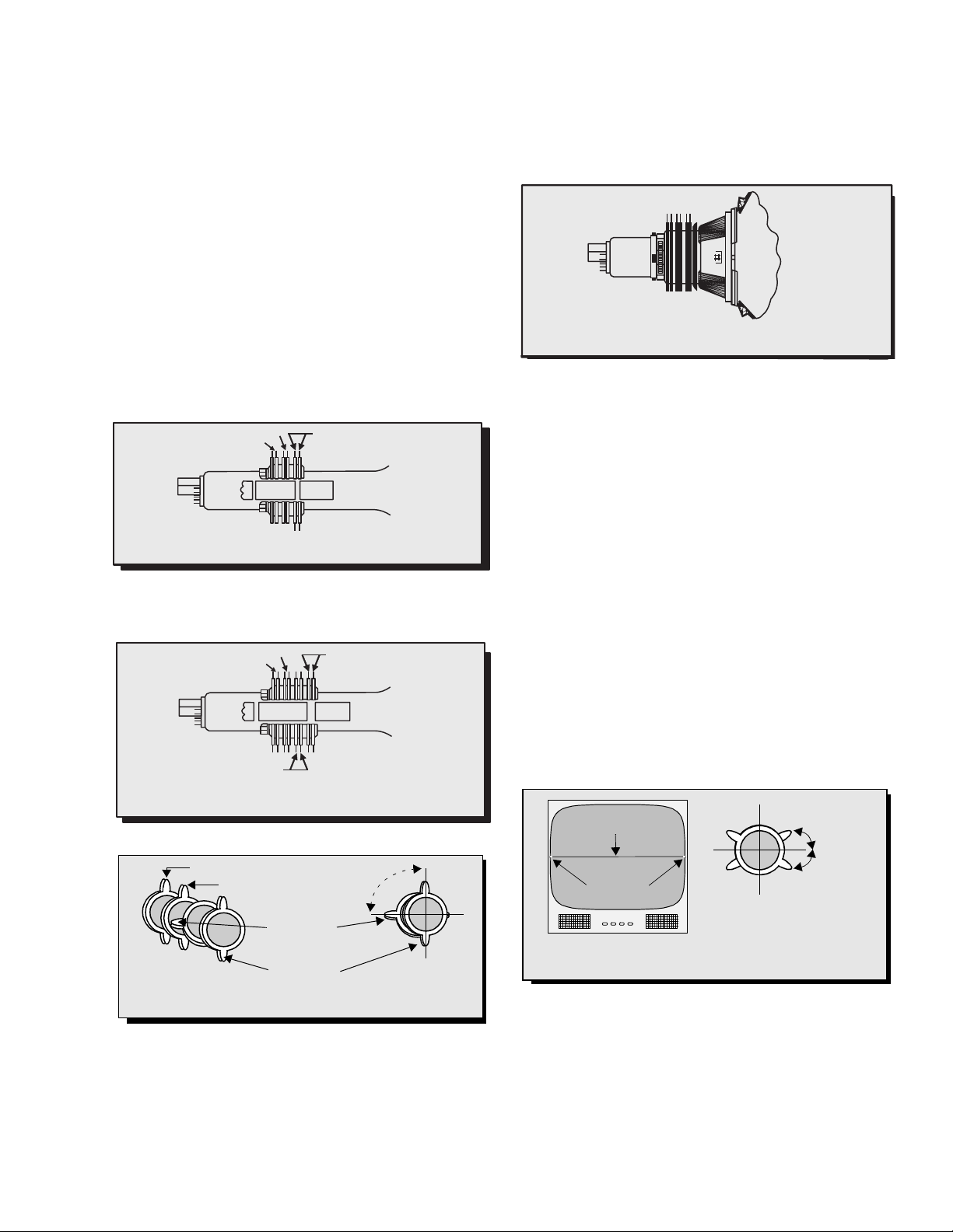
Purity and Convergence Procedure
Adjustment is necessary only if the CRT or the
deflection yoke is replaced or if the setting was
disturbed. The complete procedure consists of:
1. Vertical Raster Shift Adjustment. (Only for Models
with Purity/Convergence Assembly with 4 Pairs
of Rings).
2. Initial static convergence.
3. Setting the purity.
4. Final static convergence.
When the CRT or the Yoke is Replaced
Place the yoke on the CRT neck (do not tighten
the clamp).
For a 2-piece assembly (see Fig. 5):
Position purity/convergence assembly as shown and
tighten clamp snugly. Remove the hot-melt glue seal
on assembly and position like tabs of purity device
together at 12 o’clock to reduce its magnetic field
effect.
R&B Convergence Rings
R&B&G Convergence Rings
G3 G4
Purity Rings Centered
Over G3/G4 Gap
For a 1-piece assembly (see Fig. 8):
Position like tabs of purity devices together at 12
o’clock to reduce an y magnetic field effect. (For better
results, note part numb er and look fo r specif ications at
Service Center)
Figure 8. Positioning of Purity/Convergence
Assembly (1-piece assembly)
For either assemblies:
Turn the Receiver ON. Operate the Receiver for 60
minutes using the first Purity Check field (white screen)
to stabilize the CRT.
Fully degauss the Receiver by using an external
degaussing coil.
Slide the defle ction yoke back and forth on t he ne ck o f
the CRT until it produces a near white, uniform raster.
Figure 5. Positioning of Purity/Convergence Assembly
(2-piece assembly)
For models using 4 pairs of rings, place the vertical
raster shift tabs at 3 o’clock (90
o
from the purity and
convergence tabs, see Fig. 6 and Fig. 7)
R&B Convergence Rings
R&B&G Convergence Rings
Vertical Raster Shift Ring
G3 G4
Purity Rings Centered
Over G3/G4 Gap
Figure 6. Positioning of Purity/Convergence Assembly
(4 Pairs of Rings)
R&B&G Convergence Rings
R&B Convergence Rings
Vertical Raster
Shift Rings
Purity Rings
90
o
Figure 7. Positioning of Purity/Convergence Assembly
(4 Pairs of Rings)
Vertical Raster Shift Adjustment (Only for
Models with Purity/Convergence Assembly with 4
Pairs of Rings).
Apply a green pattern with a horizontal line, adjust the
Deflection Yoke so that has no tilt, then secure it.
Adjust center line of the pattern with the mechanical
center of the CRT, this center is determined by two
marks at the side edges of the screen. To adjust the
line, once the vertical raster shift tabs are place at 3
o’clock to reduce its magnetic field effect (see Fig. 6
and Fig. 7) open the tabs the same angle from the
center, until the center line of the pattern becomes a
straight line, center ed with the marks of the CRT. ( see
Fig. 9)
Center line
from pattern
Mechanical
Center Marks
Vertical Raster Shift tabs
Figure 9. Vertical Raster Shift Adjustment
(4 pairs of rings assembly)
Open the
same angle
from center
- 11 -
Page 12
Initial Center Static Convergence
NOTES:
1. CRT warm up with white screen
(three guns activated) is needed
to stabilize the shadow mask
expansion.
2. Initial center static convergence
(roughly centers three gun
beams) is required in order to
perform purity adjustment.
Figure 10. Green Raster Adjustment
Green Raster
Connect a dot/cross hatch generator to the Receiver
and tune in a signal. Observe misconvergence at
center of the screen o nly.
Adjust the R&B pole magne ts; by separating tabs and
rotating to converge blue with red.
Adjust the R&B and R&B&G pole magnets: by
separating tabs and rotating to converge blue an d red
(magenta) with green.
Note: Precise convergence at this point is
not important.
Purity Adjustment
When the Receiver is in the Service Mod e for making
electronic adjustments, press the Recall but ton on the
Remote Control to enter Purity Check. (See the
Service Adjustments Electronic Controls
procedure).
Operate the Receiver for 60 minutes using the first
Purity Check field (white screen) to stabilize the CRT.
Fully degauss the Receiver by using an external
degaussing coil.
Press the Recall button on the Remote Control again
until the Purity Check (green screen) appears.
For a 2-piece assembly (see Fig. 5):
Loosen the deflection yok e clamp screw an d move the
deflection yoke back as close to the purity magnet
as possible.
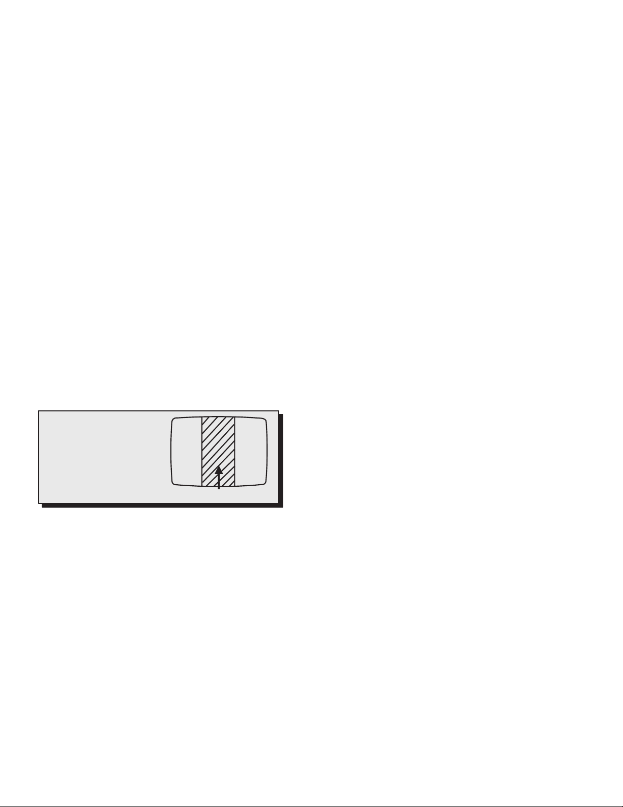
Adjust the Purit y rings to set the vertical green raster
precisely at the center of the screen (see Fig. 10).
Slowly move the deflecti on yoke forward until the best
overall green screen is displayed.
For a 1-piece assembly (see Fig. 8):
Slowly move the deflection yoke and purity rings
assembly toward the CRT board and adjust the purity
magnet rings to set vertical green raster at center of
screen (see Fig. 10).
Gradually move the deflection yoke & purity rings
forward and adjust for best overall green screen.
Continue from here for either assemblies:
Tighten the deflection yoke clamp screw.
Press the Recall button on the Remote Control again
until the purity check (blue screen) and (red screen)
appear and observe that good purity is obtained on
each respective field.
Press the Recall button on the Remote Control again
until Purity check (white screen) app ears. Obse rve the
screen for uniform white. If purity has not been
achieved, repeat the above procedure.
Final Convergence Procedure (see Fig. 11
through Fig. 13):
Note: Vertical size and focus adjustments must be
completed prior to performing the convergence
adjustment. Connect a dot pattern generator to the
Receiver. The Brightness level should not be higher
than necessary to obtain a clear pattern.
Converge the red and the blue dots at the center of the
screen by rotating the R&B pole Static Convergence
Magnets.
Align The converged red/blue dots with the green dots
at the center of the screen by rotating the R&B&G pol e
Static Convergence Magnets. Melt wax with soldering
iron to reseal the magnets.
Slightly tilt vertica lly and ho rizontally (do not ro tate) the
deflection yoke to obtain a good overall convergence.
If convergence is not reached at the edges, insert
permalloy (see fo llowing section) from the DY corners
to achieve proper convergence. Recheck for purity and
readjust if necessary.
After vertical adjustment of the yoke, insert wedge at 11
o’clock position, then make the horizontal
tilt adjustment.
Secure the deflection yoke by inserting two side
wedges at 3 and 7 o’clock positions.
Apply adhesive between tab (thin portion) of wedge
and CRT and place tape over the tab to secure to
the CRT.
Permalloy Convergence Corrector Strip (Part No. 0FMK014ZZ)
This strip is used in some sets to match the yo ke and
CRT for optimum convergence. If the y oke or CRT is
replaced, the strip may not be required.
First converge the set without the strip and observe
the corners.
If correction is needed:
1. Place strip between CRT and yoke, in quadrant
needing correction. Slowly move it around for
desired results.
2. Press adhesive tightly to the CRT and secure
with tape.
- 12 -
Page 13
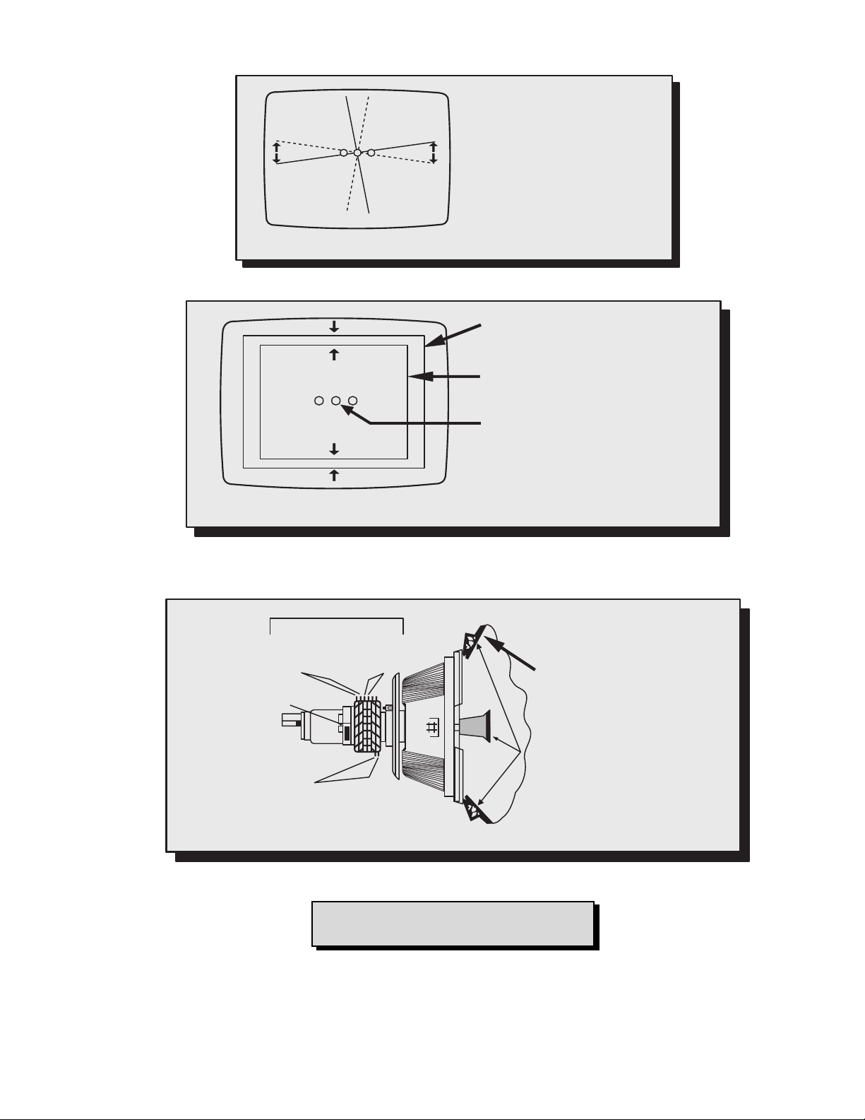
As the yoke is tilted
RGB
Figure 11. Vertical Yoke Movement
vertically, the rasters
produced by the
outside guns rotate in
opposite directions.
RGB
As the yoke is tilted horizontally, one
raster gets larger while the other gets
smaller
Figure 12. Horizontal Yoke Movement
Raster produced from one of the
outside electron beams
Raster from the other side electron
beam
Static convergence magnets are set for
center convergence
Static Convergence Magne t s
Converges
R/B with G
Purity/Convergence
Assembly Clamp
Purity Rings Adj. on
Green Raster
11 o’clock Position
Converges
R with B
Double sided adhesive tape
3 o’clock Position
Y oke Positioning Wedges
for Dynamic Convergence
7 o’clock Position
Figure 13. Convergence Magnets and Wedges Location
Note: For models using 4 pairs of rings
assemblies see Fig. 6 for details
- 13 -
Page 14
Service Mode (Electronic Controls)
This Receiver has electronic technology using the I²C Bus Concept. It performs as a control function and it
replaces many mechanical controls. Instead of adjusting mechanical controls individually, many of the control
functions are now performed by using “On Screen Display Menu”. (The Service Adjustment Mode.)
Note: It is suggested that the tech nician reads all the way through and understand the following procedur e for
Entering/Exiting the Service Adjustment Mode; then proceed with the instructions working with the
Receiver. When becoming familiar with the pr ocedur e , the Flow Chart for Ser vic e Mod e may be use d as a
quick guide.
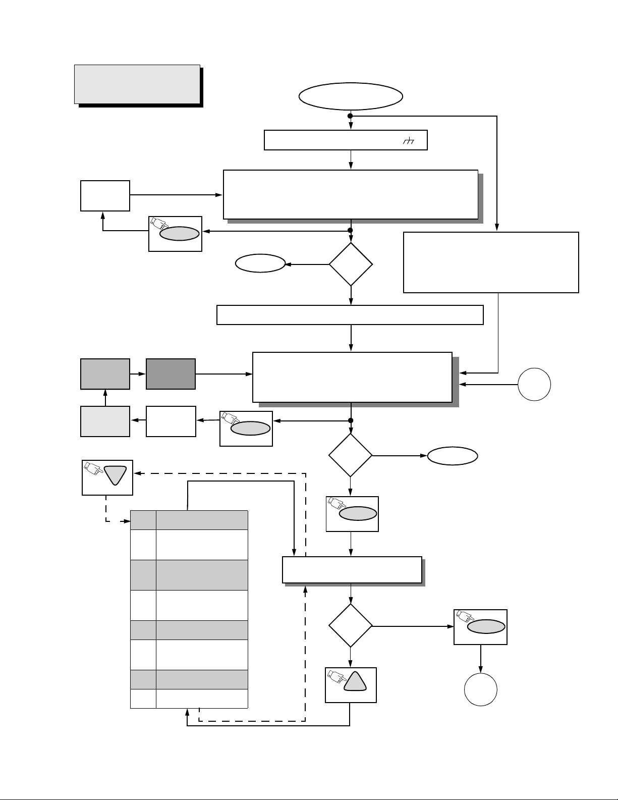
Quick Entry to Service Mode:
At times when minor adjustments need to be don e to the electronic controls, the method o f Entering the servic e
Mode without removal of the cabinet back is as follows using the Remote Control:
1. Select SET-UP icon and select CABLE mode.
2. Select TIMER icon and set SLEEP time for 30 Min.
3. Press ACTION button twice to exit menus.
4. Tune to the Channel 124.
5. Adjust VOLUME to minimum (0).
6. Press the VOL button (decrease) on Receiver. Red “CHK” appears in upper corner.
To toggle between Aging and Service modes:
While the “CHK” is displayed on the left top corner of the CRT, pressing the Action and the Volume Up buttons
on the Receiver simu ltaneously will toggle be tween the modes. Red “CHK” for Service and yellow “CHK ” for
Aging.
7. Press the Power Button on the Remote Control to select one of six Service Adjustment Modes.
1) B= Service VCJ SUB-DATA ADJUSTEMENT.
2) C= Service VCJ CUT-OFF ADJUSTMENT.
3) S= Service OPTIONS (PIP and CLOCK) ADJUSTMENT.
4) M= Service MTS ADJUSTMENTS.
5) X = Service COMB FILTER ADJUSTMENT.
6) “CHK” = Normal operation of CHANNEL and VOLUME .
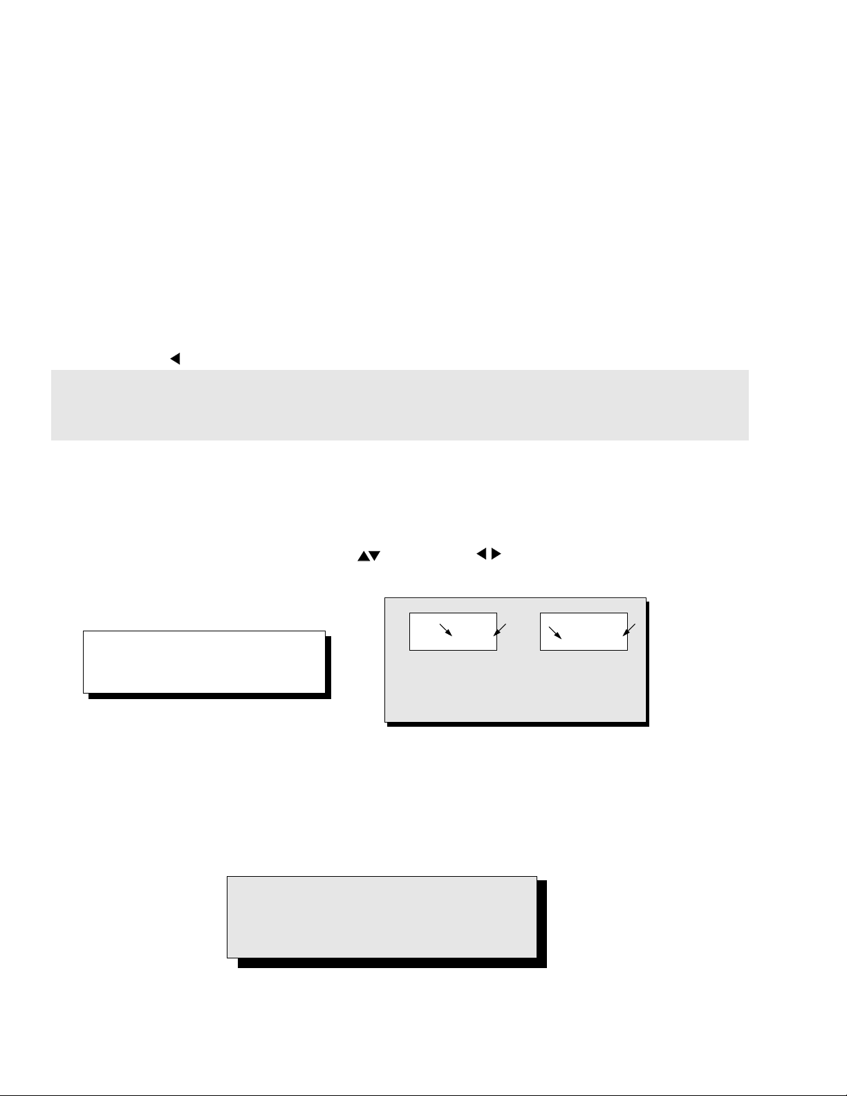
Note: Only the applicable settings for
b
32 B 0 2 215 C 0
a
b
a
the Receiver serviced will be
available (See
a
in Fig. 14).
An address Menu appears in the right
hand corner of the screen
Figure 14. Service Mode Menu Adjustments.
Exiting the Service Mode:
Press the Action and the Power buttons on the Receiver simultaneously for at least 2 seconds.
THE RECEIVER EXITS SERVICE MODE.
The Receiver momentarily shuts off; then comes back on tuned to channel 3 with a preset level of sound.
Any programmed channels, channels caption data and some others user defined settings will be erased.
IMPORTANT NOTE:
Always Exit the Service Mode
Following Adjustments.
- 14 -
Page 15
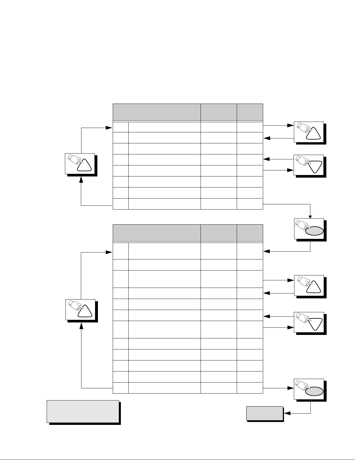
Press the Power Button on the Remote Control to select the Service Adjustment.
For Adjustments:
1.Press Channel Up/Down on the
Remote Control to select one of
the available Ser vice Adjustments
(a in Fig. 14).
Note: Write Down the original
value set (b in
Fig. 14
) for
each address before
modifying anything. It is
easy to erroneously adjust
the wrong item.
2.Press Volume Up/Down on the
Remote Control to adjust the
level of the selected Service
Adjustment (b in Fig. 14).
CH
Sub-Data Adjustment Adj. Range
B0 SUB-COLOR 0 ~ 63 43
B1 SUB-TINT 0 ~ 63 41
B2 SUB-BRIGHTNESS 0 ~ 255 49
B3 SUB-PICTURE 0 ~ 63 53
B4 KILLER/ABL/GAMMA 0 ~ 7 5
B5 VIDEO ADJUSTMENT 0 ~ 15 8
B6 AUDIO ADJUSTMENT 0 ~ 31 16
B7 V-SIZE 0 ~ 63 22
Cut-Off Adjustment Adj. Range
C0 CUT-OFF R
C1 CUT-OFF G 0 ~ 255 92
C2 CUT-OFF B
C3 DRIVE R 0 ~ 127 57
0 ~ 1
0 ~ 255
0 ~ 1
0 ~ 255
Default
Level
Default
Level
193
186
CH
CH
PW
0
0
CH
CH
IMPORTANT NOTE:
Always Exit the service Mode
Following Adjustment s .
C4 DRIVE B 0 ~ 127 57
C5 YNR SWITCH 0 ~ 1 0
C6 AFT
C7 RF-AGC 0 ~ 127 63
C8 YNR VIDEO ADJUSTMENT 0 ~ 7 0
C9 HORIZONTAL CENTER 0 ~ 31 12
Ca BEAM LIMIT 0 ~ 7 4
Cb VCJ TEST H 0 ~ 2 0
0 ~ 1
0 ~ 225
126
- 15 -
1
To S Items.
CH
PW
Page 16
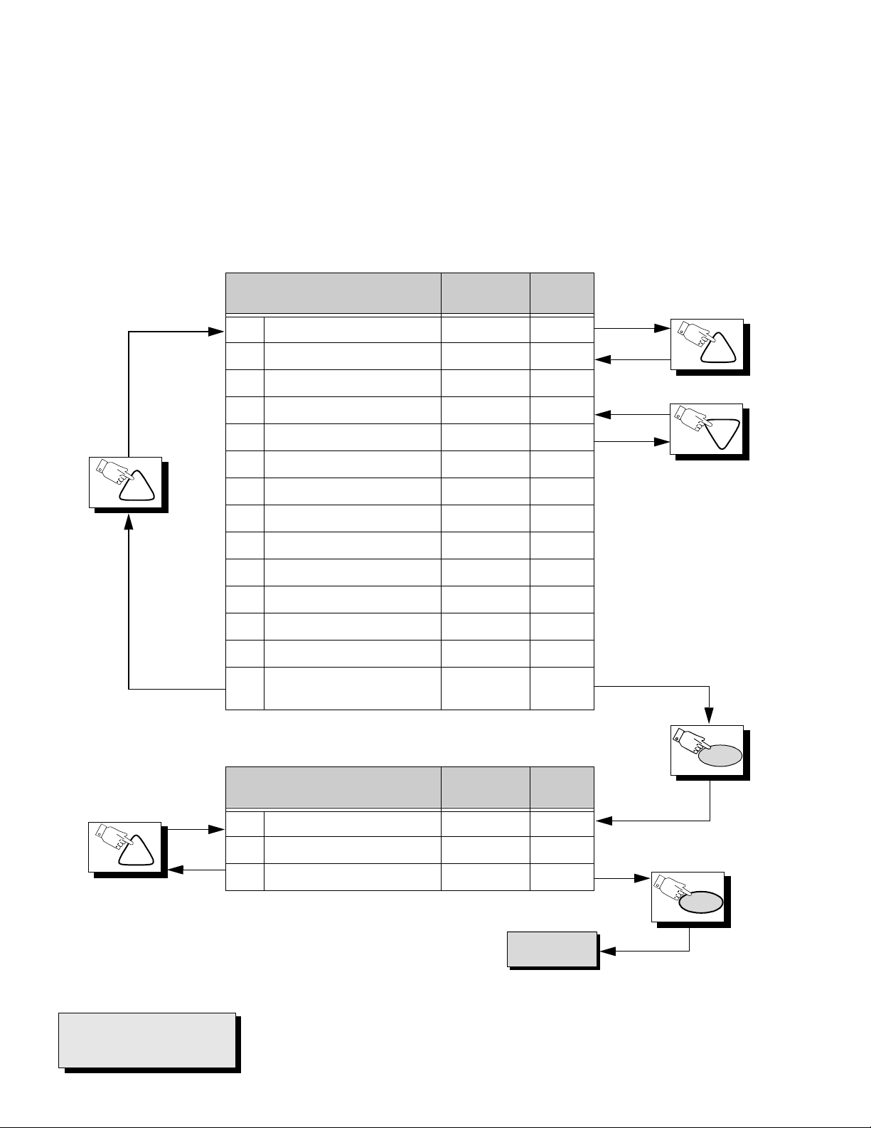
Press the Power Button on the Remote Control to select the Service Adjustment
For Adjustments:
1.Press Channel Up/Down on the
Remote Control to select one of
the available Ser vice Adjustments
(a in Fig. 14).
S0 PIP COLOR 0 ~ 127 100
S1 PIP CONTRAST 0 ~ 127 52
S2 UP 1/9 0 ~ 255 26
S3 DOWN 1/9 0 ~ 255 146
S4 LEFT 1/9 0 ~ 255 9
S5 RIGHT 1/9 0 ~ 255 103
CH
S6 UP 1/16 0 ~ 255 26
S7 DOWN 1/16 0 ~ 255 163
S8 LEFT 1/16 0 ~ 255 9
Note: Write Down the original
value set (b in
Fig. 14
) for
each address before
modifying anything. It is
easy to erroneously adjust
the wrong item.
Options Adjustment Adj. Range
2.Press Volume Up/Down on the
Remote Control to adjust the
level of the selected Service
Adjustment (b in Fig. 14).
Default
Level
CH
CH
CH
S9 RIGHT 1/16 0 ~ 255 118
Sa FREE RUN N/A N/A
Sb CLOCK ADJUSTMENT 0 ~ 255 68
Sc PIP TINT 0 ~ 63 58
Sd
M0 INPUT LEVEL 0 ~ 63 30
M1 HIGH-LEVEL SEPARATION 0 ~ 63 26
M2 LOW-LEVEL SEPARATION 0 ~ 15 11
LOUDNESS
COMPENSATION
MTS Adjustment Adj. Range
0 ~ 63 52
Default
Level
To X Items.
PW
PW
IMPORTANT NOTE:
Always Exit the Service Mode
Following Adjustments.
- 16 -
Page 17
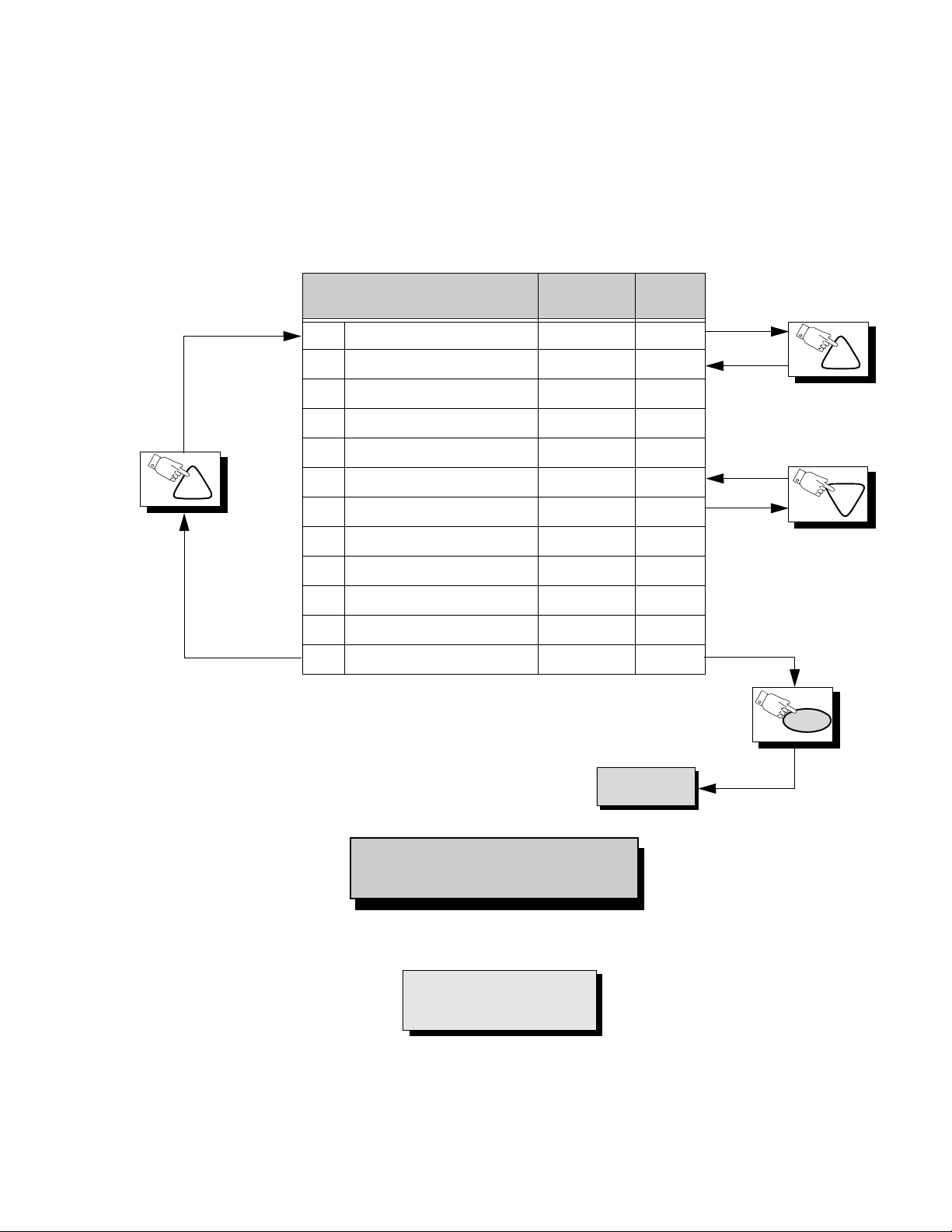
Press the Power Button on the Remote Control to select the Service Adjustment
For Adjustments:
1.Press Channel Up/Down on the
Remote Control to select one of
the available Ser vice Adjustments
(a in Fig. 14).
Note: Write Down the original
value set (b in
Fig. 14
) for
each address before
modifying anything. It is
easy to erroneously adjust
the wrong item.
2.Press Volume Up/Down on the
Remote Control to adjust the
level of the selected Service
Adjustment (b in Fig. 14).
CH
Comb Filter Adjustment Adj. Range
X0 COMB GAIN 0 ~ 255 152
X1 COMB SWITCH 0 ~ 63 12
X2 COMB LIMIT 0 ~ 63 24
X3 COMB CORE 0 ~ 127 41
X4 COMB RF DELAY 0 ~ 127 18
X5 COMB VIDEO DELAY 0 ~ 127 18
X6 COMB VMLM 0 ~ 127 90
X7 COMB VM SW 0 ~ 63 24
X8 CO MB SHARP 0 ~ 255 30
X9 COMB VM LEVEL 0 ~ 255 255
Xa CO MB VMPKF 0 ~ 1 1
Xb COMB ADJ SHARP 0 ~ 63 10
Default
Level
CH
CH
PW
To B Items.
Note: Some adjustments modes may not be
available in some models depending
on available options.
IMPORTANT NOTE:
Always Exit the Service Mode
Following Adjustments.
- 17 -
Page 18
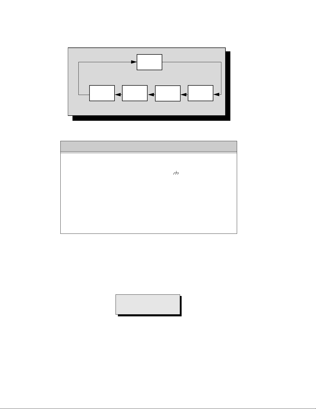
To Check Purity:
Press the Recall Button on the Remote Control when in Service Mode (red “CHK” is displayed) to enter the Purity
Field Check Mode.
NORMAL
SCREEN
Press Recall again to select desired field.
BLUE
SCREEN
GRN.
SCREEN
RED
SCREEN
WHITE
SCREEN
Figure 15. Purity Check Field Mode.
Helpful Hints
Entering Service Mode (Back-Open Method)
1. While the Receiver is ON and operati ng in Normal M ode, momentarily
short test point FA1 (TP8) to Cold Ground ( ) FA2 (TP3) A-Board.
The Receiver enters the Aging Mode
Yellow letters “CHK” appear in the upper left corner of the CRT.
(The Volume Up/Down will adjust rapidly).
2. Simultaneously press the Action and the Volume Up buttons on the
Receiver Control Panel.
The Receiver enters the Service Mode.
The letter in “CHK” turn red.
(The Volume Up/Down will adjust normally).
(All customer controls are set to nominal level).
.
IMPORTANT NOTE:
Always Exit the Service Mode
Following Adjustments.
- 18 -
Page 19
IMPORTANT NOTE:
Always Exit the Service Mode
Following Adjustments.
WHITE
SCREEN
Instructional Flow Chart for Service Mode
NORMAL MODE
Momentary short FA1 to FA2 ( ).
AGING MODE
• Yellow “CHK” appears in upper left corner of screen.
• Volume Up/Down operate rapidly.
• Customer Controls are set to nominal level.
GRN.
SCREEN
RED
SCREEN
CH
(ON REMOTE)
RECALL
(ON REMOTE)
BLUE
SCREEN
WHITE
SCREEN
B7 V-SIZE
B6
B5
AUDIO
ADJUSTMENT
VIDEO
ADJUSTMENT
QUICK ENTRY TO SERVICE MODE
• Select CABLE Mode.
•Set SLEEP time for 30 Min.
• Tune to Channel 124.
• Adjust Volume to minimum.
• Press VOL DOWN On Receiver.
EXIT
N
Adj.
needed?
Y
Press Action + Volume Up Simultaneously (ON Receiver)
SERVICE MODE
• “CHK” turns red.
• Volume Up/Down operate normally.
• Customer Controls are set to nominal level.
RECALL
(ON REMOTE)
Adj.
needed?
N
EXIT
Y
POWER
(ON REMOTE)
SUB-DATA ADJUSTMENTS.
B ITEMS.
B
B4
B3 SUB-PICTURE
B2
B1 SUB-TINT
B0 SUB-COLOR
KILLER/ABL/
GAMMA
SUB-
BRIGHTNESS
Adj.
needed?
N
Y
CH
(ON REMOTE)
Figure 16.Flow Chart for Service Mode.
- 19 -
POWER
(ON REMOTE)
A
Page 20
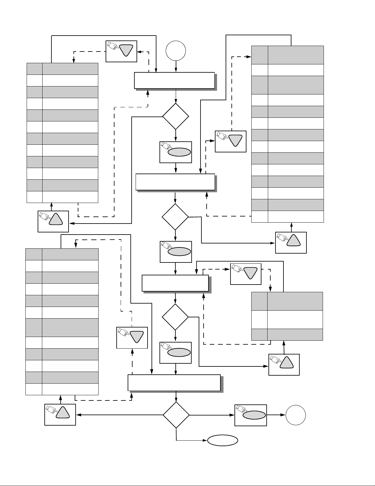
Instructional Flow Chart for Service Mode - Continued
Cb VCJ TEST
Ca BEAM LIMIT
C9 HORIZ CENTER
C8 YNR VID ADJ
C7 RF-AGC
C6 AFT
C5 YNR SWITCH
C4 DRIVE B
C3 DRIVE R
C2 CUT-OFF B
C1 CUT-OFF G
C0 CUT-OFF R
CH
(ON REMOTE)
Xb COMB ADJ SHARP
Xa COMB VMPKF
X9 COMB VM LEVEL
X8 COMB SHARP
X7 COMB VM SW
X6 COMB VMLM
X5
X4 COMB RF DELAY
X3 COMB CORE
X2 COMB LIMIT
X1 COMB SWITCH
X0 COMB GAIN
COMB VIDEO
DELAY
CH
(ON REMOTE)
(ON REMOTE)
A
CUT-OFF ADJUSTMENTS.
C ITEMS.
Y
Adj.
needed?
N
POWER
(ON REMOTE)
OPTIONS ADJUSTMENTS.
S ITEMS.
Y
Adj.
needed?
N
POWER
(ON REMOTE)
MTS ADJUSTMENTS.
M ITEMS.
Adj.
Y
POWER
CH
needed?
N
(ON REMOTE)
COMB-FILTER ADJUSTMENTS.
X ITEMS.
(ON REMOTE)
CH
CH
(ON REMOTE)
Sd
Sc PIP TINT
Sb
Sa FREERUN
S9 RIGHT 1/16
S8 LEFT 1/16
S7 DOWN 1/16
S6 UP 1/16
S5 RIGHT 1/9
S4 LEFT 1/9
S3 DOWN 1/9
S2 UP 1/9
S1 PIP CONTRAST
S0 PIP COLOR
M2
M1
M0 INPUT LEVEL
LOUDNESS
COMPENSATION
CLOCK
ADJUSTMENT
CH
(ON REMOTE)
LOW-LEVEL
SEPARATION
HIGH-LEVEL
SEPARATION
CH
(ON REMOTE)
CH
(ON REMOTE)
Adj.
Y
needed?
N
(ON REMOTE)
N
EXIT
Figure 17. Flow Chart for Service Mode.(Continued)
- 20 -
POWER
B
Page 21
Service Adjustments (Electronic Controls)
Sub-Brightness
Service DAC Adjustment (B2)
Adjustment of this control is important for setting proper
operation of custome r brightness and picture cont rols.
This adjustment must be made after Sub-Contrast or
Color Temperature adjustments are made. Do not
adjust SCREEN after the Sub-Brightness is set.
Preparation:
Apply a color ba r signal wit 100 IRE white and 7.5
IRE black. (Switch Color to “OFF” on the signal
generator.) Operate the Receiver for a m inimum o f
10 minutes prior to performing this adjustment.
Procedure:
In the Service Mode for making electronic
adjustments, select the DAC adjustment (B2) and
adjust until the black starts to look gray. Then
decrease the level to the point where gray turns
to black.
Note: You may set the accurate value following the
Preparation steps and the Procedure s tep No.
2 of the Sub-Contrast adjustment described
below.
Video Adjustment Level
Service DAC Adjustment (B5)
Preparation:
1. Obtain an NTSC color bar pattern with 100 IRE
white and 87.5% modulation.
2. Connect the oscilloscope to TP12. Use cold
ground for scope connection. Set the scope at
Horizontal Sweep rate (20µs) time base.
Procedure:
1. In the Service Mode for making electronic
adjustments, select DAC Video Adjustment Level
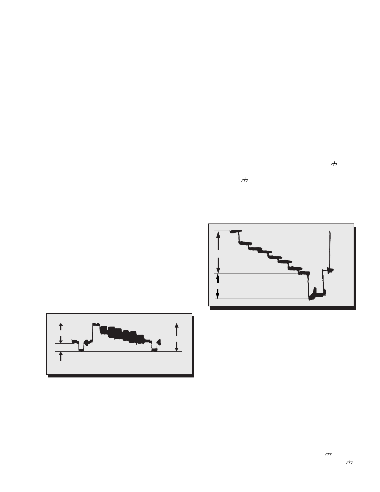
(B5) and adjust for 1.0±0.05V from sync ti p to white
level. See Fig. 18.
P
S
1V ±0.05V
Preparation:
1. Apply a color bar signal pattern with 87.5%
modulation, 70% saturated color bar with a 100
IRE white and 7.5 black.
Note:
The pattern us ed in this proced ure is an EIA color
bar pattern with 87.5% modulation with 100 IRE
white and 7.5 black. Correlate the information in this
procedure to the pattern used if another signal
is used.
2. Preset the following controls:
• Brightness . . . . . . . .Center.
• Color . . . . . . . . . . . .Min.
• Picture . . . . . . . . . . .Max.
• Sharpness . . . . . . . .Center.
3. Connect the oscilloscope to the CRT-Board
connector C1-2. Set the scope time base to 20µs
(horizontal).
4. Connect a jumper from TPD2 to ground ( ).
5. Connect a jumper from IC101 pin 28 to
ground ( ).
Procedure:
1. In the Service Mode, select DAC Sub-Brightness
Adjustment (B2) and adjust for 1.0-1.5Vp-p
between blanking and 7.5 IRE level. (See video
waveforms detail, Fig. 19).
White
Yellow
Cyan
Green
2.8V
±0.1V
p-p
1V - 1.5V
p-p
Magenta
Red
Blue
Black
SYNC
TIP
Figure 19. TP47G waveform
2. In the Service Mode for electronic adjustments,
select DAC Sub-Contrast Adjustment (B3) and
adjust for 2.8Vp-p ±0.1V for 27” models from whit e
level to black level on video waveform (see video
waveforms detail, Fig. 19).
3. Remove the jumpers (Preparation steps 4 & 5).
Figure 18. TP12 waveform
2. Check that the sync signal amplitude (ratio
between the sync signal to detection output) is
within the range of 30 ±5% (S/(S+P) = 30 ±5%).
3. Set the DAC Sub-Contrast Adjustment (B3).
Sub-Contrast
Service DAC Adjustment (B3)
This adjustment is factory set. Do not adjust unless
repairs are made to as sociated circui t, the CRT Board
or when the CRT is replaced.
Tint/Color Adjustment
Service DAC Adjustment (B1) (B0)
Preparation:
1. Apply a rainbow color bar signal.
2. Preset the following controls:
• Brightness . . . . . . . .Min.
• Color . . . . . . . . . . . .Center.
• Tint. . . . . . . . . . . . . .Center.
• Picture . . . . . . . . . . .Max.
• Sharpness . . . . . . . .Min.
3. Connect the oscilloscope to TP47B (A-Board).
4. Connect a jumper from TPD2 to GND ( ).
5. Connect a jumper from IC101 pin 28 to GND ( ).
- 21 -
Page 22
Service Adjustments (Electronic Controls, cont.)
A to B = 1 unit
A
C
1 2 3 10
4 5 6 7 8 9
B
B to C = 2 units
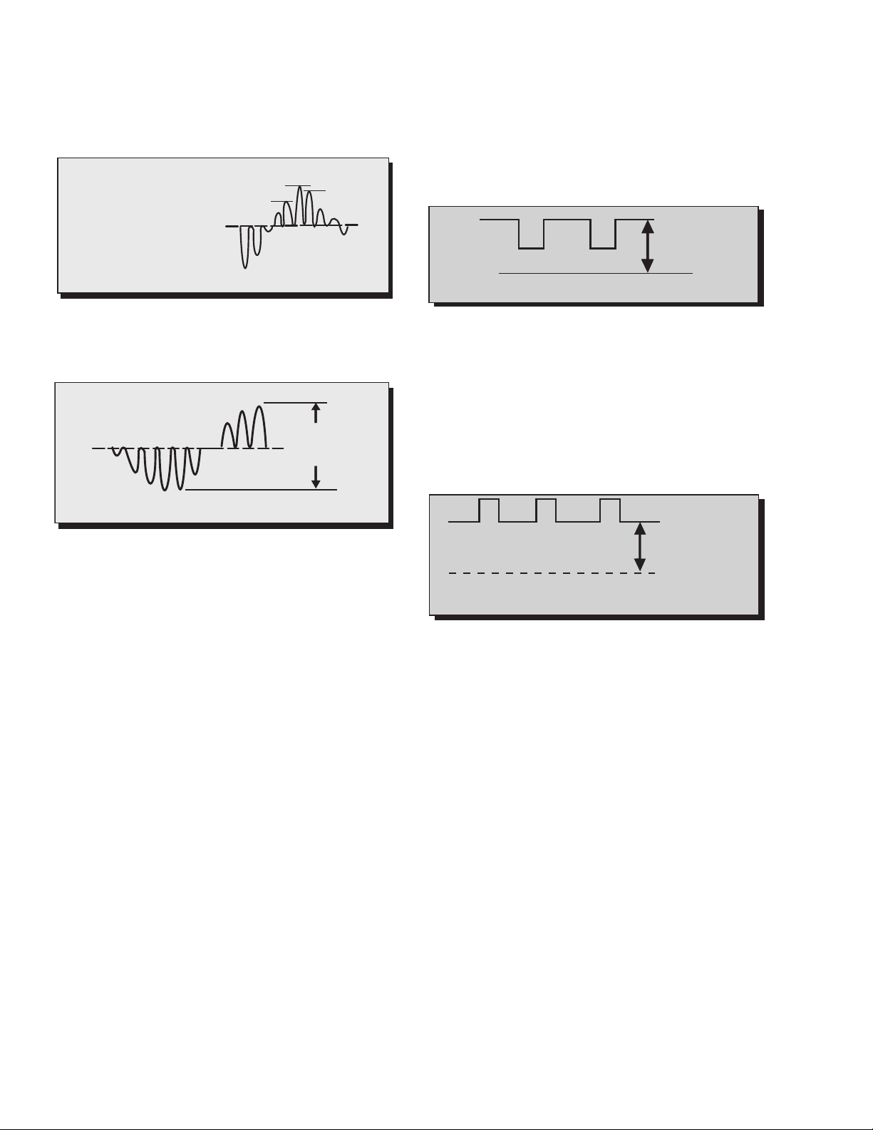
Figure 20. TP47B waveform
TP47B (A-Board)
1 2 3 4 5 6
7 8 9 10
Figure 21. TP47G waveform
TP47G (A-Board)
0.9Vp-p±0.05V
Procedure:
1. In the Service Mode for making electronic
adjustments, select DAC Sub-Tint Adjustment
(B1). Adjust until the wav eform me asur ed is as th e
one shown in Fig. 20.
2. Connect the oscilloscope to TP47G (A-Board).
3. Select DAC Sub-Color Adjustm ent (B0) and adjust
for peak to peak amplitud e to be 0.9Vp-p ±0.05V
for 27” models as shown in Fig. 21.
1. Connect the oscilloscope to C1-2 (CRT-Board).
2. In Service Mode for maki ng electronic adjust ment,
select the Sub-Bright DAC (B2).
3. Press the R-Tune key on the remote.
4. Observe the oscilloscope waveform at Horizontal
rate and adjust the Service Mode Sub-Bright DAC
(B2) level until a scanning period of 3.1V above DC
ground is measured, as indicated in Fig. 22.
3.1V DC
0V DC
Figure 22. TP36 Waveform
5. Connect the scope to G RN Cathode (KG) on the
CRT-Board.
6. In the Service Mode for making electronic
adjustments, select the GREEN CUTOFF
DAC (C1).
7. Press the R-Tune key on the remote.
8. View scope trace at Horizontal r ate and adjust the
Service Mode DAC (C1) level until a scanning
period of 160V above DC g round is measured, as
indicated in Fig. 23.
4. Remove the jumpers (Preparation steps 4 & 5).
Color Temperature Adjustment
(B/W Tracking)
Service DAC Adjust. (C0) (C1) (C2) (C3) (C4)
Minor Touch-Up Method
OBSERVE low and high brightness areas of a B/W
picture for proper tracking. Adjust only as required for
“good gray scale and warm highlights”.
1. LOW LIGHT areas – In S ervice Mode for making
electronic adjustments, select Cutoff (C0) RED,
(C1) GRN, (C2) BLU and adjust the picture for
gray.
2. HIGH LIGHT areas – In Service Mode for mak ing
electronic adjustments, select Drive (C3) RED,
(C4) BLU and adjust the picture for warm whites.
Complete Adjustment
Preparation:
1. Turn the Receiver “ON” and allow 10 minutes
warm up at h igh brightness.
2. Apply a color bar signal with color “OFF”.
3. Turn the SCREEN control (part of FBT T551) fully
counterclockwis e.
Procedure:
Preset the following Service DACs for best results:
• C0. . . . . . . . . 0 128
• C1. . . . . . . . . . . 64
• C2. . . . . . . . . 0 128
• C3. . . . . . . . . . . 64
• C4. . . . . . . . . . . 64
160V DC
0V DC
Figure 23. Cathode Waveform, Adjustment
9. Connect the scope to the RED Cathode (KR).
10. In Service Mode for making electronic adjustments,
select the RED CUTOFF DAC (C0).
11. Press the R-Tune key on the Remote
12. View the sco pe trace an d adjust the Servic e Mode
DAC (C0) for the scanning period to be 160V
above DC ground. (See Fig. 23)
13. Connect the scope to the BLU Cathode (KB).
14. In Service Mode for making electronic adjustments,
select the BLU CUTOFF (C2).
15. Press the R-Tune key on the Remote.
16. View the sco pe trace an d adjust the Servic e Mode
DAC (C2) for the scanning period to be 160V
above DC ground. (See Fig. 23)
17. Turn the Screen Control (part of FBT) slowly
clockwise until a color horizontal line appears.
18. With the other two colors Service Mode DAC
CUTOFF adjustments (C0) RED, (C2) BLU;
increase the colors to create a white horizontal line.
19. Confirm that a good gray scale is established by
viewing B/W color bar pattern.
- 22 -
Waveform Detail
(Ground)
Page 23
Service Adjustments (Electronic Controls, cont.)
20. In the Service Mode for making electronic
adjustments select the DAC DRIVE adjustments
(C3) RED, (C4) BLUE and adjus t for warm whi te i n
a white color bar pattern.
21. EXIT the Service Mode.
22. Adjus t the Pictur e Menu Video Adj ustmen ts Bright
and Picture from low sc ale t o hi gh s cale and chec k
Black and White tracking.
23. If correction is needed: Re-Enter the Service Mode
and perform the Minor Touch – Up Method.
24. Perform Sub-Brightness Adjustm ent procedure if
needed.
Horizontal Centering
Service DAC Adjustment (C9)
Preparation:
Connect a monoscope pattern.
Procedure:
1. In the Service Mode for making electronic
adjustments. Select the Horizontal Centering
Adjustment DAC (C9) and ad ju st un til the c ent er of
the crosshatch pattern is centered on CRT.
2. EXIT the Service Adjustment Mode.
Audio Adjustment
Service DAC Adjustment (B6)
This adjustment is factory set and needs to be
performed only when IC002 or IC101 is replaced.
Preparation:
1. Apply the following signal at the antenna (70dB
±5dB, 75Ω open P/S 10dB): audio signal set to
monaural, 300Hz. 100% modul ation; video inpu t of
100 IRE flat field, 30% modulation.
2. Connect the RMS Meter with filt er jig as shown in
Fig. 24.
RMS
METER
4700p
Figure 24. Filter Jig
Procedure:
1. In the Service Mode for making electronic
adjustments, select the Audio Adjustment DAC
(B6) and adjust until 75mV RM S ±5.0m V RMS is
measured.
2. EXIT the Service Adjustment Mode.
10k
TPE1
(A-BOARD)
MTS Circuit Adjustments
The MTS Circuit Adjustments require two steps:
1. Input Level Adjustment.
2. Stereo Separation Adjustment.
Input Level Adjustment (M0)
Preparation:
1. Connect an RMS meter with filter jig as shown in
Fig. 25.
RMS
METER
10k
TPE10
4700p
Figure 25. Filter Jig
2. Connect an RF signal generator to the RF
antenna input.
Procedure:
1. Apply the following signal from the RF signal
generator:
Video: 100 IRE flat field, 30% modulation.
Audio: 300Hz, 100% modulation, monaural
(70 ±5dB, 75Ω OPEN, P/S 10dB).
2. Adjust the MTS In put Level Adjustment (M0) until
the voltage measured is 106 ± 6.0mV rms.
Stereo Separation Adjustment (M1 & M2)
Preparation:
1. Connect an RF s ign al gener a tor to the RF an tenn a
input.
2. Connect a scope to TPE10.
Procedure:
1. Select Stereo Mode in Audio menu
2. Apply the following signal from the RF signal
generator:
Video: 100 IRE flat field, 30% modulation.
Audio: 300Hz, 100% modu lation, stereo (left onl y)
(70 ±5dB, 75Ω OPEN, P/S 10dB).
3. Adjust the MTS Low-Le vel Separation Adjustment
(M2) until the amplitude displayed on the scope
is minimum.
4. Apply the following signal from the RF
signal generator:
Video: 100 IRE flat field, 30% modulation.
Audio: 3KHz, 100% modulation, stereo (left only)
(70 ±5dB, 75Ω OPEN, P/S 10dB).
5. Adjust the MTS H igh-Level Separation Adjus tment
(M1) until the amplit ude displayed on the scope is
minimum
6. .Repeat above steps 2 through 5 until the
amplitude is at minimum for both signals.Service
Adjustments (Electronic Controls, cont.)
- 23 -
Page 24
Clock Adjustment (Sb)
Preparation:
Connect the frequency co unter from TPS1 (IC001
Pin 13) to cold ground ( ).
Note: Frequency Counter pr obe capacitance should
be 8pF or less.
Procedure:
1. Turn the Receiver “OFF” with the AC
power applied.
2. Measure TPS1 (IC001 pin 13) for the frequency of
the waveform and record the reading.
Note: Pin 13 measurement must have at least four
digits of resolution following the de cimal point.
Example: 000.0000
3. Turn the Receiver back “ON”.
4. Place the Receiver in to Service Mode for making
electronic adjustment , select th e Clock A djustment
DAC (Sb).
Service Adjustmen ts (Mechanical Controls)
5. Calculate and set Sb based on the
followingformula:
pin
244.1406
Sb 128 0.9016×10
Note: Pin 13 measurement will not change
regardless of the value stored in Sb.
----------------------------------------------------------------- -+=
244.1406
13 Hz[]–{}
V ertical Size (B7)
1. Adjust the VERTICAL SIZE DA C control, B7, until
the top and the bottom edges of the raster are
visible.
2. Adjust the VERTICAL SIZE control, B7, until the
top and the bottom of the raster touch the bezel
edge. The advance SIZE control to obtain an
approximately 10% oversc an. Linearity adj ustment
is done automatically when the size is being
adjusted. (Best results can de obtained with a
round test patter.)
VCO Field Alignment L105 (IC101 pins 35 & 36)
1. Connect a balance antenna a nd select a midband
channel (Ch 10, 11 or 12)
2. Attenuate the signal strength for a weak noisy
video.
3. While observing the pic ture tube, adjust L105 un til
best picture appears.
4. Change channels and observe tha t they are tuning
properly.
5. If the channel monitor ed is not clear, repeat steps
1, 3 and 4 while applying a stronger signal.
Focus (part of T551)
Preparation:
Connect a Signal generator and select a do tpattern.
Procedure:
Adjust the FOCUS cont rol to obtain the sharpest and
clearest dot pattern.
a. Adjust for best center.
b. Adjust for best area between the center and top
right corner.
E-W Pincushion
Perform H-Centering adjustment to confirm correct
picture centering.
Preparation:
Apply a crosshatc h patte r n.
H- Width Adjustment
Perform H-Centering adjustment to confirm correct
picture centering.
Preparation:
Apply a monoscope pattern.
Procedure:
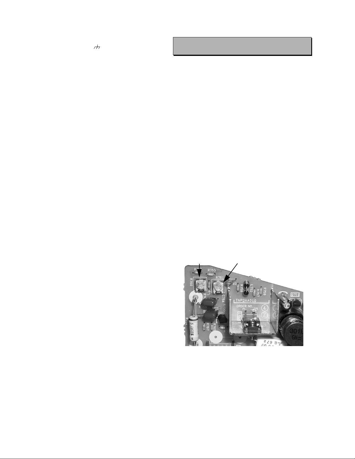
Adjust R760 and B7 until obtain a perfect round pattern
on the screen.
R760
R761
Z-BOARD
Procedure:
Adjust E-W Pincush ion by adjusting R761 on Z-Boa rd
until outside vertical lines are as straight as possible.
- 24 -
Page 25
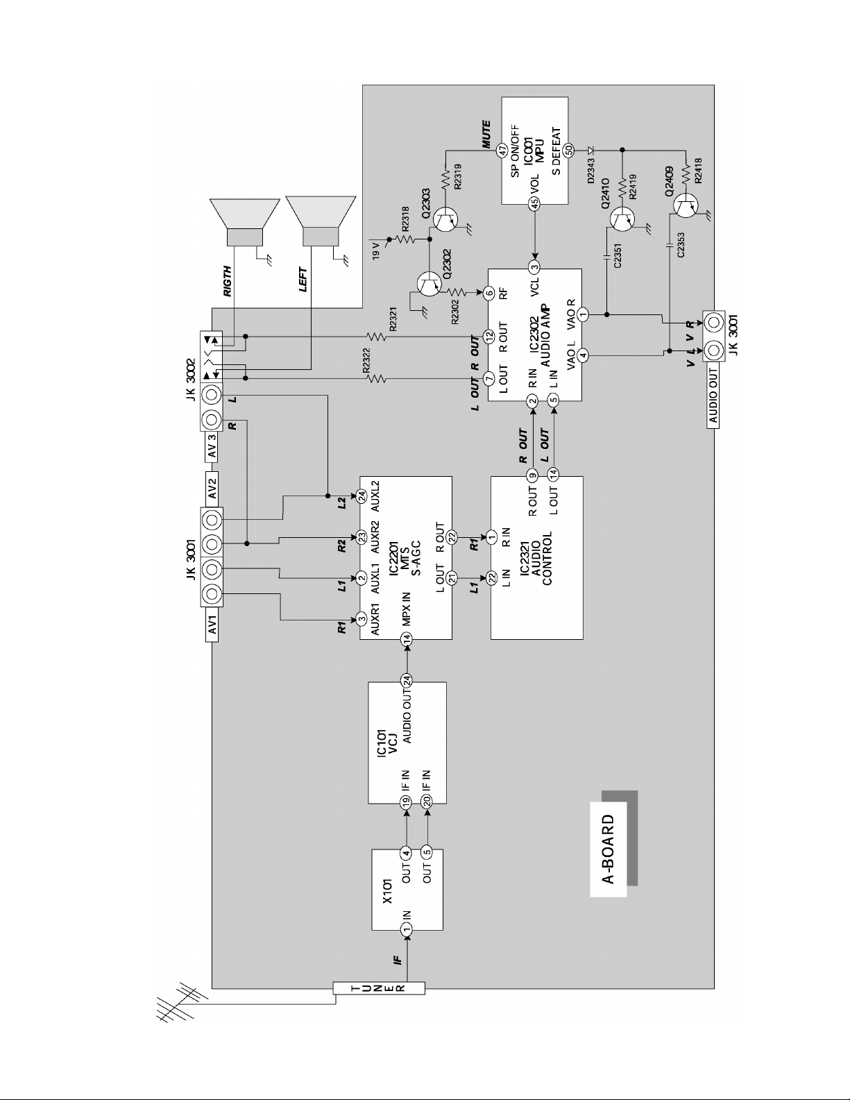
Audio Signal Path Block Diagram
Figure 26. Audio Signal Path Block Diagram.
- 25 -
Page 26
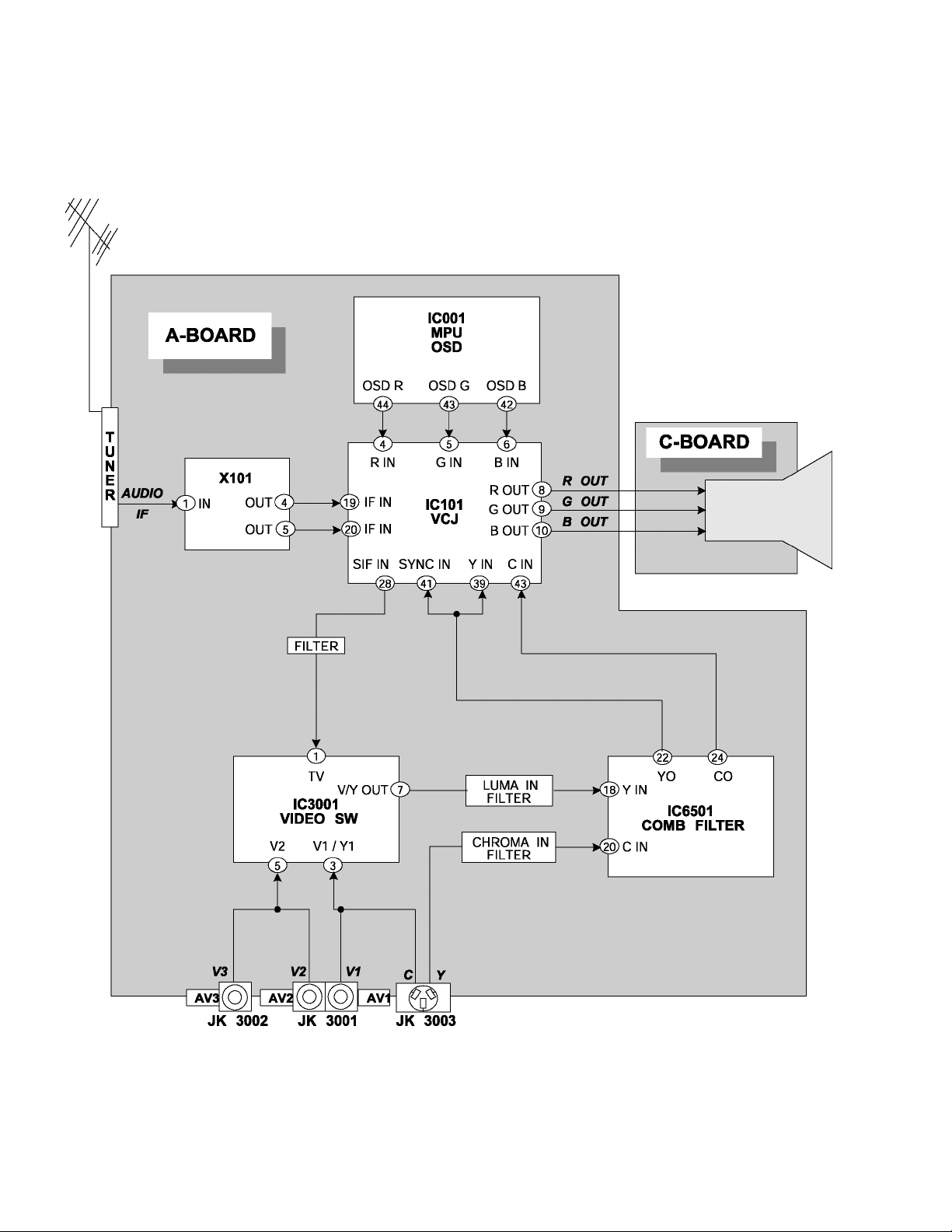
Video-Chroma Signal Path Block Diagram
Figure 27. Video-Chroma Path Block Diagram.
- 26 -
Page 27
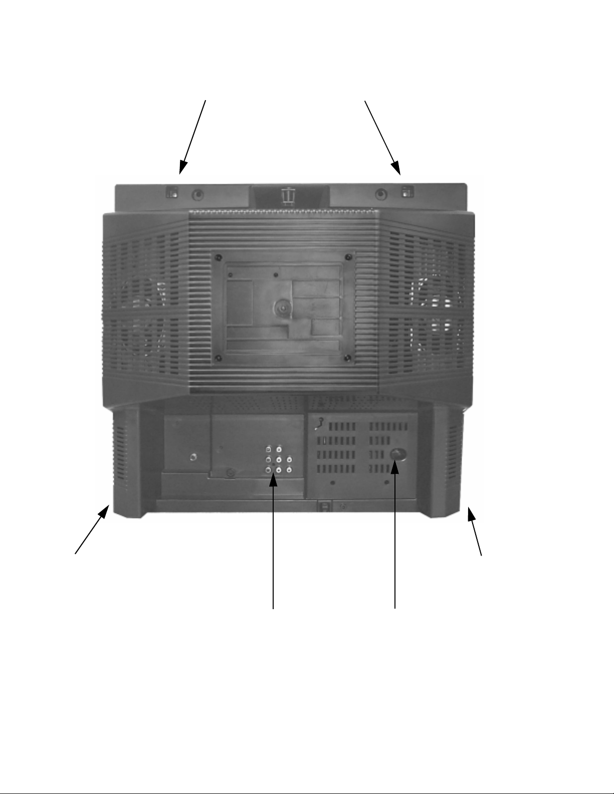
Identification of Components
2 screws at the top edge of the receiver
1 screw at the lower
edge of the receiver
1 screw by the
A/V jacks
Figure 28. Back Cover Removal
- 27 -
1 screw by the
flyback assembly
1 screw at the lower
edge of the receiver
Page 28
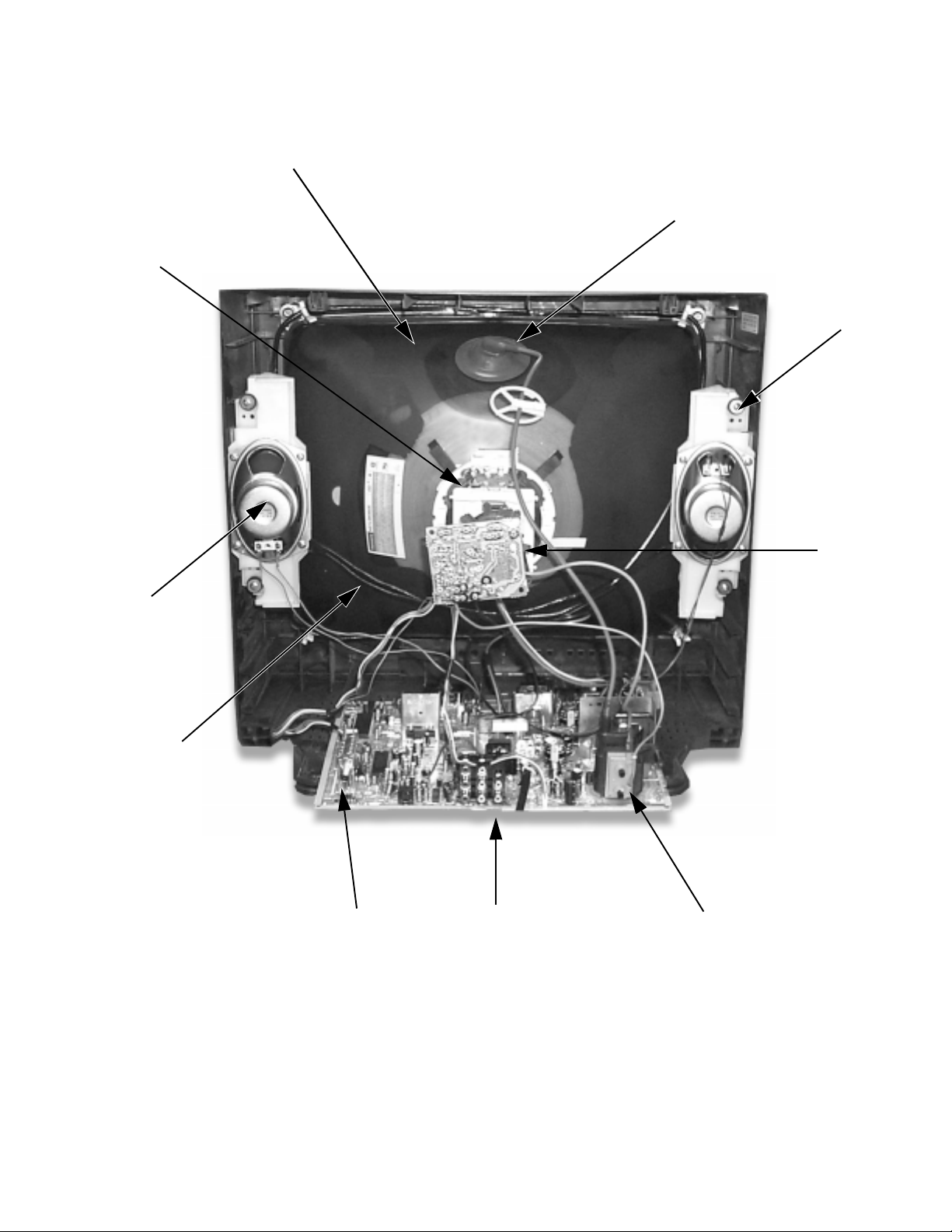
Yoke
Identification of Components
CRT (secured to cabinet by
4 screws on corners of CRT)
Anode (high voltage)
Speaker Bracket
(2 screws)
Speaker
(4 screws)
Degaussing
coil
Tuner A/V jacks Flyback (T551)
Note:
remember to dress the cables, as shown.
After servicing the receiver,
C board
Figure 29. Rear View
- 28 -
Page 29
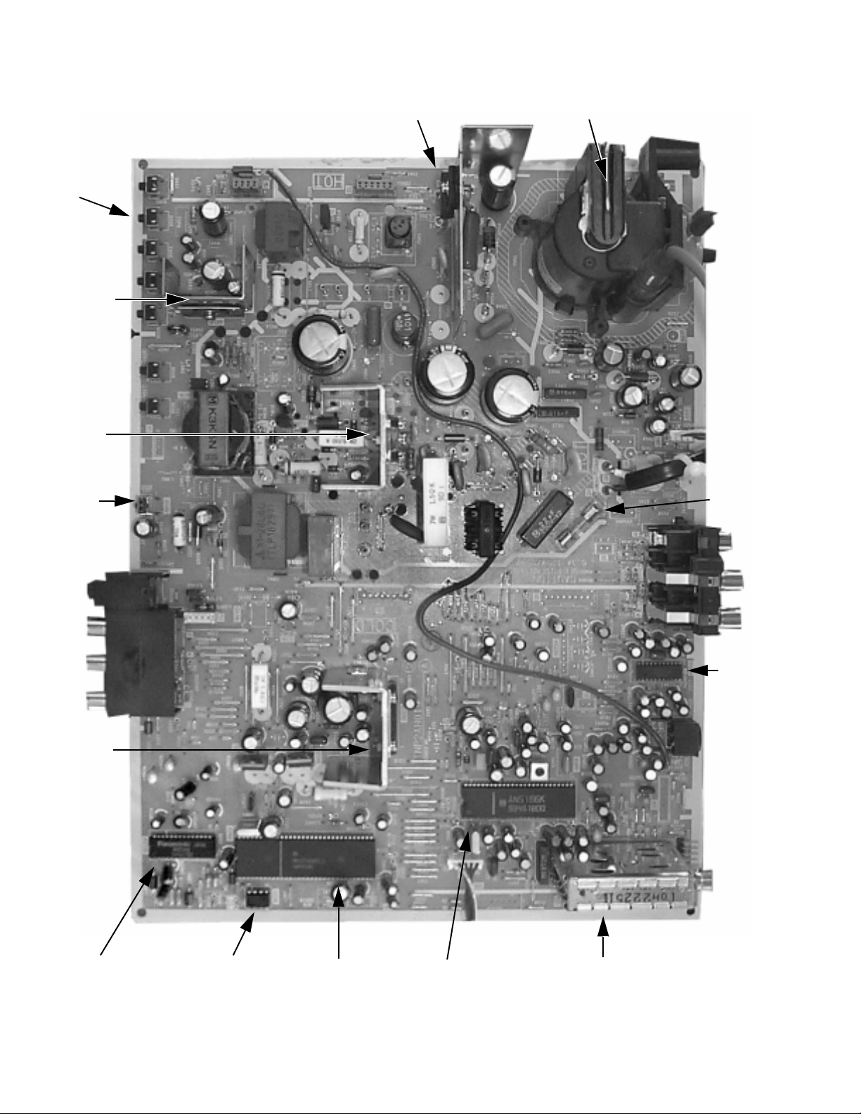
Identification of Components
KEYPAD
IC451
V. OUT
IC803
POWER S.
IC003
SENSOR
Q551
H. OUT
T551
FBT
F801
FUSE
IC2302
AUDIO AMP
IC6501
COMB FILTER
IC002
EEPROM
IC101
VCJ
Figure 30. A-Board Main Components
IC001
MPU
IC2321
AUDIO
TNR001
TUNER
- 29 -
Page 30
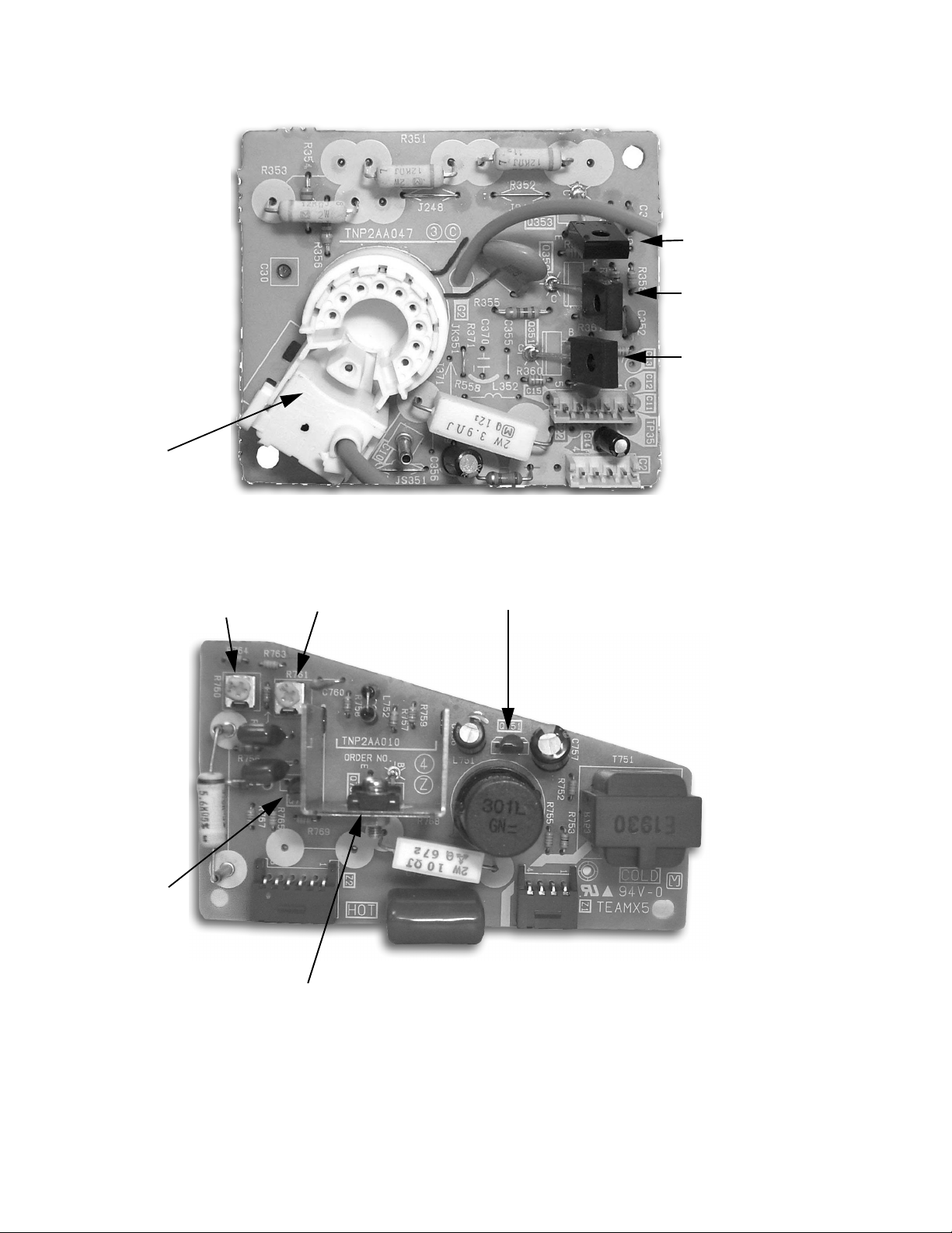
C-BOARD
CRT SOCKET
Identification of Components
Q353
Q352
Q351
Z-BOARD
Q752
R760 R761 Q751
Q753
Figure 31. Component Identification, C&Z Boards
- 30 -
Page 31
REPLACEMENT PARTS LIST
Model:CT-20SX11E/CE
Important Safety Notice: Components printed in BOLD TYPE have special characteristics important for safety. When replacing
any of these components use only manufacturer’s specified parts.
REF NO. PART NO. DESCRIPTION
C604 TCJ2VU1H150J CAP,C 15PF-J-5 0V
C605 TCJ2VB1H332K CAP,C .0033UF-K-50V
C606 ECA1HM010B CAP,E 1UF-50V
C754 ECQB1H104JFW CAP,P .1UF-J-50V
C755 ECQB1H104JFW CAP,P .1UF-J-50V
C756 ECA1CM221B CAP,E 10UF-16V
C757 ECA1VM221B CAP,E 220UF-35V
C759 ECQE1395KNB CAP,P 3.95UF-K-100V
C760 TACCV101T50V CAP,C 100PF/50V
C801 ECKWAE472ZED CAP,C 4700PF-Z-500V
C802 ECKWAE472ZED CAP,C 4700PF-Z-500V
C803 ECKWAE472ZED CAP,C 4700PF-Z-500V
C804 ECKWAE472ZED CAP,C 4700PF-Z-500V
C805 EC0S2DG151DG CAP,E 151UF/200V
C806 EC0S2DG151DG CAP,E 151UF/200V
C807 ECA1HM2R2B CAP,E 2.2UF-50V
C808 ECA1CM101B CAP,E 100UF/16V
C809 EC0S2DG151DG CAP,E 151UF/200V
C810 ECQU2A153MVA CAP,P .015UF-M-250VAC
C811 ECQU2A153MVA CAP,P .015UF-M-250VAC
C812 ECQU2A224MVA CAP,P .22UF-M-250VAC
C814 ECQB1H823JM3 CAP,P .082UF-J-50V
C815 ECA1HHG470B CAP,E 47UF-50V
C818 ECKW3A821KBP CAP,C 820PF-K-1KVDC
C820 ECA1JHG100B CAP,E 10UF-63V
C821 ECKR2H561KB5 CAP, C 560PF-K- 500V
C822 ECA1EM221B CAP,E 220UF-25V
C823 ECA160V33UE CAP,E 33UF/160V
C824 ECKW3A331KBP CAP,C 330PF-K-1KV
C825 ECKW3A471KBP CAP,C 470PF-K-1KV
C2201 ECA1HM4 R7B CAP,E 4.7UF-50V
C2202 ECA1HM2R2B CAP,E 2.2UF-50V
C2203 ECA1HM4 R7B CAP,E 4.7UF-50V
C2204 AP106K016CAE CAP,T 10UF/16V
C2205 ECA1HM010B CAP,E 1UF-50V
C2206 ECQB1H223JM 3 CAP, P .022UF- J-50V
C2207 AP335K016CAE CAP,T 3.3UF/16V
C2208 TCJ2VB1C104K CAP,C .1UF-K-16V
C2209 TCJ2VB1C104K CAP,C .1UF-K-16V
C2210 TCJ2VB1C104K CAP,C .1UF-K-16V
C2212 ECQB1H473JM 3 CAP,P .047UF-J-50V
C2215 ECA0JM 101B CAP,E 100UF-6.3V
C2218 ECA1HMR 47B CAP,E .47UF-50V
C2220 EEANA 1E100B CAP,E 10UF-25V
C2301 ECA1VM 102E CAP,E 1000UF-35V
C2302 ECA1HM010B CA P,E 1UF-50V
C2305 ECA1HM0 10B CAP,E 1UF-50V
C2306 TCJ2VF1H103Z CAP,C .01UF-Z-50V
C2307 ECA1CM1 02B CAP,E 1000UF/16V
C2309 ECQB1H473JM 3 CAP, P .047UF- J-50V
C2311 ECA1HM2 R2B CAP,E 2.2UF-50V
REF NO. PART NO. DESCRIPTION
C2313 ECA1EM 101B CAP,E 100UF-25V
C2314 ECQB1H473JM 3 CAP,P .047UF- J-50V
C2315 ECA1EM 100B CAP,E 10UF-25V
C2321 ECA1EM 100B CAP,E 10UF-25V
C2324 ECA1EM 100B CAP,E 10UF-25V
C2325 ECA1CM 102B CAP,E 1000UF/16V
C2331 EEANA 1E100B CAP,E 10UF-25V
C2332 EEANA 1E100B CAP,E 10UF-25V
C2333 ECA1HM 0R1B CAP,E 0.1UF/50V
C2334 TCJ2VB1H472K CA P,C 4700PF-K-50V
C2335 ECA1AM 470B CAP,E 47UF-10V
C2336 ECQB1H104JM 3 CAP,P .1UF- J-50V
C2337 ECA1HM 0R1B CAP,E 0.1UF/50V
C2338 ECA1EM 4R7B CAP,E 4.7UF/25V
C2339 ECA1CM 100B CAP,E 10UF-16V
C2340 ECA1HM R47B CA P,E .47UF-50V
C2341 ECA1EM 4R7B CAP,E 4.7UF/25V
C2342 ECA1EM 4R7B CAP,E 4.7UF/25V
C2343 ECA1EM 4R7B CAP,E 4.7UF/25V
C2344 TCJ2VB1H472K CA P,C 4700PF-K-50V
C2345 ECA1HM 0R1B CAP,E 0.1UF/50V
C2346 ECA1AM 470B CAP,E 47UF-10V
C2347 TCJ2VF1H103Z CAP,C .01UF-Z-50V
C2351 ECA1HM 010B CAP,E 1UF-50V
C2353 ECA1HM 010B CAP,E 1UF-50V
C2359 ECA1HM 010B CAP,E 1UF-50V
C2360 ECA1HM 010B CAP,E 1UF-50V
C2362 ECA1AM 470B CAP,E 47UF-10V
C3011 ECA1HM010B CAP,E 1UF-50V
C3012 ECA1HM 010B CAP,E 1UF-50V
C3013 ECA1CM 100B CAP,E 10UF-16V
C3014 ECA1CM 100B CAP,E 10UF-16V
C3018 ECA1HM 010B CAP,E 1UF-50V
C3019 ECA1HM 010B CAP,E 1UF-50V
C3025 ECA1HM 100B CAP,E 10UF/50V
C3234 ECA1AM 470B CAP,E 47UF-10V
C3240 TCJ2VF1H103Z CAP,C .01UF-Z-50V
C6501 ECEA1C KA101B CAP,E 100UF-16V
C6502 TCJ2VF1H103Z CAP,C .01UF-Z-50V
C6503 TCJ2VF1H103Z CAP,C .01UF-Z-50V
C6504 TCJ2VC1H270J CAP,C 27PF-J-50V
C6507 TCJ2VC1H120J CAP,C 12PF-J-50V
C6508 TCJ2VC1H390J CAP,C 39PF-J-50V
C6509 TCJ2VC1H270J CAP,C 27PF-J-50V
C6510 TCJ2VC1H120J CAP,C 12PF-J-50V
C6511 ECEA1H KA010B CAP,E 1.0UF-50V
C6512 TCJ2VF1H103Z CAP,C .01UF-Z-50V
C6513 TCJ2VC1H270J CAP,C 27PF-J-50V
C6514 TCJ2VF1H103Z CAP,C .01UF-Z-50V
C6515 TCJ2VC1H101J CAP,C 100PF-J-50V
C6516 TCJ2VF1H103Z CAP,C .01UF-Z-50V
PARTS LIST
192-01
- 32 -
Parts List
Page 32
REPLACEMENT PARTS LIST
Model:CT-20SX11E/CE
Important Safety Notice: Components printed in BOLD TYPE have special characteristics important for safety. When replacing
any of these components use only manufacturer’s specified parts.
REF NO. PART NO. DESCRIPTION
C6517 ECEA1HN 010UB CAP,E 1UF/50V
C6518 TCJ2VF1H103Z CAP,C .01UF-Z-50V
C6520 ECEA1CKA100B CAP,E 10UF-16V
C6521 ECEA1CK A470B CAP,E 47UF-16V
C6522 TCJ2VC1H221J CAP,C 220PF-J-50V
C6523 TCJ2VF1H104Z CAP,C .1UF-Z-50V
C6524 ECEA1HKA010B CAP,E 1.0UF-50V
C6525 TCJ2VF1H103Z CAP,C .01UF-Z-50V
C6526 ECEA1CKA100B CAP,E 10UF-16V
C6527 TCJ2VF1H104Z CAP,C .1UF-Z-50V
C6528 ECEA1CKA470B CAP,E 47UF-16V
C6529 ECEA1CK A100B CAP,E 10UF-16V
C6531 TCJ2VF1H103Z CAP,C .01UF-Z-50V
C6532 TCUV1H103KBN CAP,C .01UF-K-50V
DIODES
D001 ERA15-01V3 DIODE, RECTIFIER
D002 MA165TA5VT DIODE, SWITCHING
D003 MA4047HTA DIODE
D006 MA4330HTA DIODE
D008 MA165TA5VT DIODE, SWITCHING
D009 MA165TA5VT DIODE, SWITCHING
D011 MA165TA5VT DIODE, SWITCHING
D014 MA165TA5VT DIODE, SWITCHING
D015 MA165TA5VT DIODE, SWITCHING
D016 MA165TA5VT DIODE, SWITCHING
D017 MA165TA5VT DIODE, SWITCHING
D026 MA4056MTA DIODE
D451 ERA15-01V3 DIODE, RECTIFIER
D452 MA4047MTA DIODE
D453 MA165TA5VT DIODE, SWITCHING
D461 MA27WTA DIODE
D501 MA4082LTA DIODE
D531 AS01V0 DIODE
D532 MA4062LTVTA DIODE, ZENER
D551 TVSRU2NV1 DIODE, SILICONE
D554 BYD33G-163 DIODE
D555 MA165TA5VT DIODE, SWITCHING
D556 MA4360HTA DIODE, ZENER
D557 TVSRU2NV1 DIODE, SILICONE
D558 RS3FS DIODE
D559 BYD33G-113 DIODE
D560 MA165TA5VT DIODE, SWITCHING
D561 BYD33G-163 DIODE
PARTS LIST
D751 MA2270B DIODE
D801 GP15KL-042 DIODE
D802 GP15KL-042 DIODE
D806 MA4056MTA DIODE
D807 MA165TA5VT DIODE, SWITCHING
D809 RU3YX-MV1 DIODE, RECTIFIER
D810 TAP2A102M005 DIODE (THERMISTOR)
D820 EU02V1 DIODE
REF NO. PART NO. DESCRIPTION
D821 EU02V1 DIODE
D822 EU02V1 DIODE
D823 RL30A DIODE
D824 EU02V1 DIODE
D825 TVSSR2KLV1 DIODE, PROTECTION
D826 EU02V1 DIODE
D829 MA165TA5VT DIODE, SWITCHING
D830 MA4270MTA DIODE
D2301 MA165TA5VT DIODE, SWITCHI NG
D2305 MA4110MTA DIODE, ZENER
D2306 MA4110MTA DIODE, ZENER
D2307 MA4110MTA DIODE, ZENER
D2308 MA4110MTA DIODE, ZENER
D2315 MA165TA5VT DIODE, SWITCHING
D2342 MA165TA5VT DIODE, SWITCHI NG
D2343 MA165TA5VT DIODE, SWITCHING
D3001 MA4110MTA DIODE, ZENER
D3002 MA4110MTA DIODE, ZENER
D3003 MA4110MTA DIODE, ZENER
D3004 MA4110MTA DIODE, ZENER
D3005 MA4110MTA DIODE, ZENER
D3006 MA4110MTA DIODE, ZENER
D3007 MA4110MTA DIODE, ZENER
D3008 MA4110MTA DIODE, ZENER
D3009 MA4110MTA DIODE, ZENER
D3010 MA4110MTA DIODE, ZENER
D3011 MA4110MTA DIODE, ZENER
D3012 MA4110MTA DIODE, ZENER
D3017 MA4110MTA DIODE, ZENER
D3018 MA4110MTA DIODE, ZENER
D3019 MA4110MTA DIODE, ZENER
D3020 MA4110MTA DIODE, ZENER
D3021 MA4110MTA DIODE, ZENER
D3022 MA4110MTA DIODE, ZENER
FUSES
F801 XBA2A00101 FUSE 6.3A 125V
INTEGRATED CIRCUITS
IC001 MN1874088TL3 MPU
IC002 C3EAEC000016 EEPROM
IC003 PIC-37042SR REMOTE SENSOR
IC101 AN5166K VCJ
IC451 LA7837-TV V OUT
IC551 AN78M09LB 9 VOLT REG.
IC552 AN78M05LB PL US 5V AVR
IC801 PC817X2 OPTHO COUPLER
IC803 STR58041A POWER SUPPLY
IC2201 AN5829S-E1V MTS
IC2302 AN5272 AUDIO AMP
IC2321 CXA2021S AUDIO CONTROL
IC3001 MM1114XFBE VIDEO SW
IC6501 MN82840 COMB FILTER
Parts List
- 33 -
192-01
Page 33
REPLACEMENT PARTS LIST
Model:CT-20SX11E/CE
Important Safety Notice: Components printed in BOLD TYPE have special characteristics important for safety. When replacing
any of these components use only manufacturer’s specified parts.
REF NO. PART NO. DESCRIPTION
IC6502 PST9142NR RESET
COILS
JS08 EXCELSA35V FERRITE BEAD
L001 EXCELSA35V FERRITE BEAD
L002 ELESN2R2KA COIL, PEAKING 2.2UH
L003 TLTABT2R2K COIL, PEAKING 2.2UH
L004 TLTABT2R2K COIL, PEAKING 2.2UH
L006 EXCELSA24T FERRITE BEAD
L008 TLTABT470K COIL, PEAKING 47UH
L103 ELESN150JA COIL, PEAKING 15UH
L104 TLUABTA390K COIL, PEAKING 39UH
L105 EIV7EN053B COIL, VCO
L106 ELESN180JA COIL, PEAKING 18UH
L451 EXCELDR35V FERRITE BEAD
L551 ELH5L4101 COIL
L554 EXCELSA24T FERRITE BEAD
L555 EXCELSA24T FERRITE BEAD
L556 EXCELSA24T FERRITE BEAD
L751 ELC18B501E COIL
L752 EXCELDR35V FERRITE BEAD
L801 ELF15N013A LINE FILTER
L804 EXCELSA39V FERRITE BEAD
L805 EXCELSA39V FERRITE BEAD
L2302 TLTABT2R2K COIL, PEAKING 2.2UH
L2303 EXCELDR25V FERRITE BEAD
L2304 EXCELDR25V FERRITE BEAD
L2305 EXCELDR35V FERRITE BEAD
L6502 ELESN150JA COIL, PEAKING 15UH
L6504 ELESN330JA COIL, PEAKING 33UH
L6505 ELESN330JA COIL, PEAKING 33UH
L6507 EXCELDR25V FERRITE BEAD
L6509 EXCELSA35V FERRITE BEAD
TRANSISTORS
Q001 2SD601ARTX TRANSISTOR
Q002 2SC1685QRSTA TRANSISTOR
Q003 2SB709ARTX TRANSISTOR
Q004 2SB709ARTX TRANSISTOR
Q302 2SD601ARTX TRANSISTOR
Q303 2SB709ARTX TRANSISTOR
Q304 2SD601ARTX TRANSISTOR
Q351 2SC3063RL TRANSISTOR
Q352 2SC3063RL TRANSISTOR
Q353 2SC3063RL TRANSISTOR
Q430 2SD601ARTX TRANSISTOR
Q451 2SD601ARTX TRANSISTOR
Q452 2SD601ARTX TRANSISTOR
Q501 2SC4212HLB TRANSISTOR
Q551 2SD2499LBMA2 TRANSISTOR
Q751 2SC1685QRSTA TRANSISTOR
Q752 2SA564AQRSTA TRANSISTOR
Q753 2SD1266PLB TRANSISTOR
REF NO. PART NO. DESCRIPTION
Q801 2SC1685RSTA TRANSISTOR
Q802 2SC1384RS TRANSISTOR
Q2302 2SB709ARTX TRANSISTOR
Q2303 2SD601ARTX TRANSISTOR
Q2362 2SB709ARTX TRANSISTOR
Q2363 2SD601ARTX TRANSISTOR
Q2409 2SD601ARTX TRANSISTOR
Q2410 2SD601ARTX TRANSISTOR
Q6501 2SD601ARTX TRANSISTOR
Q6502 2SD601ARTX TRANSISTOR
Q6503 2SD601ARTX TRANSISTOR
Q6504 2SD601ARTX TRANSISTOR
Q6505 2SD601ARTX TRANSISTOR
Q6506 2SD601ARTX TRANSISTOR
Q6507 2SD601ARTX TRANSISTOR
Q6509 2SD601ARTX TRANSISTOR
Q6510 2SB709ARTX TRANSISTOR
Q6516 2SB709ARTX TRANSISTOR
Q6517 2SD601ARTX TRANSISTOR
Q6519 2SD601ARTX TRANSISTOR
RELAYS
RL801 TSEH8007 RELAY
RESISTORS
R002 ERJ6GEYJ182V RES,M 1.8K-J-1/10W
R003 ERJ6GEYJ562V RES,M 5.6K-J-1/10W
R004 ERDS1TJ181T RES,C 180-J-1/2W
R005 ERDS2TJ101T RES,C 100-J-1/4W
R006 ERJ6GEYJ102V RES,M 1K-J-1/10W
R007 ERJ6GEYJ102V RES,M 1K-J-1/10W
R008 ERJ6GEYJ562V RES,M 5.6K-J-1/10W
R009 ERJ6GEYJ221V RES,M 220-J-1/10W
R010 ERJ6GEYJ104V RES,M 100K-J-1/10W
R011 ERJ6GEYJ474V RES,M 470K-J-1/10W
R012 ERJ6GEYJ473V RES,M 47K-J-1/10W
R013 ERJ6GEYJ223V RES,M 22K-J-1/10W
R014 ERJ6GEYJ472V RES,M 4.7K-J-1/10W
R015 ERJ6GEYJ472V RES,M 4.7K-J-1/10W
R016 ERJ6GEYJ472V RES,M 4.7K-J-1/10W
R017 ERJ6GEYJ472V RES,M 4.7K-J-1/10W
R020 ERJ6GEYJ474V RES,M 470K-J-1/10W
R021 ERJ6GEYJ101V RES,M 100-J-1/10W
R022 ERJ6GEYJ101V RES,M 100-J-1/10W
R023 ERJ6GEYJ102V RES,M 1K-J-1/10W
R024 ERJ6GEYJ221V RES,M 220-J-1/10W
R025 ERJ6GEYJ223V RES,M 22K-J-1/10W
R027 ERJ6GEYJ103V RES,M 10K-J-1/10W
R030 ERJ6GEYJ102V RES,M 1K-J-1/10W
R031 ERJ6GEYJ471V RES,M 470-J-1/10W
R032 ERJ6ENF1002V RES,M 10K-F-1/10W
R033 ERJ6GEYJ222V RES,M 2.2K-J-1/10W
R034 ERJ6GEYJ222V RES,M 2.2K-J-1/10W
PARTS LIST
192-01
- 34 -
Parts List
Page 34
REPLACEMENT PARTS LIST
Model:CT-20SX11E/CE
Important Safety Notice: Components printed in BOLD TYPE have special characteristics important for safety. When replacing
any of these components use only manufacturer’s specified parts.
REF NO. PART NO. DESCRIPTION
R035 ERJ6GEYJ332V RES,M 3.3K-J-1/10W
R036 ERJ6GEYJ562V RES,M 5.6K-J-1/10W
R037 ERJ6GEYJ103V RES,M 10K-J-1/10W
R038 ERJ6GEYJ223V RES,M 22K-J-1/10W
R039 ERJ6GEYJ102V RES,M 1K-J-1/10W
R040 ERJ6GEYJ223V RES,M 22K-J-1/10W
R043 ERJ6GEYJ223V RES,M 22K-J-1/10W
R044 ERJ6GEYJ471V RES,M 470-J-1/10W
R046 ERJ6GEYJ103V RES,M 10K-J-1/10W
R048 ERJ6GEYJ221V RES,M 220-J-1/10W
R049 ERJ6GEYJ221V RES,M 220-J-1/10W
R052 ERJ6GEYJ103V RES,M 10K-J-1/10W
R055 ERJ6GEYJ103V RES,M 10K-J-1/10W
R057 ERJ6GEYJ103V RES,M 10K-J-1/10W
R060 ERJ6GEYJ102V RES,M 1K-J-1/10W
R065 ERJ6GEYJ471V RES,M 470-J-1/10W
R066 ERJ6GEYJ222V RES,M 2.2K-J-1/10W
R067 ERJ6GEYJ222V RES,M 2.2K-J-1/10W
R068 ERJ6GEYJ222V RES,M 2.2K-J-1/10W
R101 ERJ6GEYJ750V RES,M 75-J-1/10W
R102 ERJ6GEYJ683V RES,M 68K-J-1/10W
R103 ERJ6GEYJ183V RES,M 18K-J-1/10W
R104 ERJ6GEYJ561V RES,M 560-J-1/10W
R105 ERJ6GEYJ561V RES,M 560-J-1/10W
R107 ERJ6GEYJ471V RES,M 470-J-1/10W
R108 ERJ6GEYJ222V RES,M 2.2K-J-1/10W
R152 ERJ6GEYJ183V RES,M 18K-J-1/10W
R153 ERJ6GEYJ223V RES,M 22K-J-1/10W
R154 ERJ6GEYJ393V RES,M 39K-J-1/10W
R201 ERJ6GEYJ471V RES,M 470-J-1/10W
R202 ERJ6GEYJ682V RES,M 6.8K-J-1/10W
R203 ERJ6GEYJ222V RES,M 2.2K-J-1/10W
R303 ERJ6GEYJ682V RES,M 6.8K-J-1/10W
R304 ERJ6GEYJ332V RES,M 3.3K-J-1/10W
R305 ERJ6ENF3001V RES,M 3K-F-1/10W
R306 ERJ6ENF1651V RES,M 1.65K-F-1/10W
R307 ERJ6GEYJ394V RES,M 390K-J-1/10W
R308 ERJ6GEYJ102V RES,M 1K-J-1/10W
R309 ERJ6GEYJ333V RES,M 33K-J-1/10W
R310 ERJ6GEYJ333V RES,M 33K-J-1/10W
R311 ERJ6GEYJ185V RES,M 1.8MEG-J-1/10W
R313 ERJ6GEYJ471V RES,M 470-J-1/10W
R314 ERJ6GEYJ102V RES,M 1K-J-1/10W
PARTS LIST
R317 ERJ6GEYJ684V RES,M 680K-J-1/10W
R320 ERJ6GEYJ102V RES,M 1K-J-1/10W
R351 ERG2FJ123H RES,M 12K-J-2W
R352 ERG2FJ123H RES,M 12K-J-2W
R353 ERG2FJ123H RES,M 12K-J-2W
R354 ERDS1TJ272T RES,C 2.7K-J-1/2W
R355 ERDS1TJ272T RES,C 2.7K-J-1/2W
R356 ERDS1TJ272T RES,C 2.7K-J-1/2W
REF NO. PART NO. DESCRIPTION
R357 ERDS2TJ331T RES,C 330-J-1/4W
R358 ERDS2TJ331T RES,C 330-J-1/4W
R359 ERDS2TJ331T RES,C 330-J-1/4W
R360 ERDS2TJ122T RES,C 1.2K-J-1/4W
R361 ERDS2TJ122T RES,C 1.2K-J-1/4W
R362 ERDS2TJ122T RES,C 1.2K-J-1/4W
R363 ERDS2TJ101T RES,C 100-J-1/4W
R364 ERDS2TJ101T RES,C 100-J-1/4W
R365 ERDS2TJ101T RES,C 100-J-1/4W
R401 ERJ6GEYJ102V RES,M 1K-J-1/10W
R430 ERJ6GEYJ103V RES,M 10K-J-1/10W
R432 ERJ6GEYJ102V RES,M 1K-J-1/10W
R451 ERDS1FJ1R2P RES,C 1.2-J-1/2W
R454 ERJ6GEYJ473V RES,M 47K-J-1/10W
R455 ERJ6GEYJ153V RES,M 15K-J-1/10W
R456 ERJ6GEYJ562V RES,M 5.6K-J-1/10W
R457 ERJ6GEYJ182V RES,M 1.8K-J-1/10W
R458 ERJ6GEYJ273V RES,M 27K-J-1/10W
R459 ERJ6GEYJ683V RES,M 68K-J-1/10W
R460 ERDS2TJ102T RES,C 1K-J-1/4W
R462 ERJ6GEYJ473V RES,M 47K-J-1/10W
R463 ERJ6GEYJ473V RES,M 47K-J-1/10W
R465 ERJ6GEYJ103V RES,M 10K-J-1/10W
R466 ERJ6GEYJ103V RES,M 10K-J-1/10W
R467 ERJ6GEYJ104V RES,M 100K-J-1/10W
R468 ERJ6GEYJ101V RES,M 100-J-1/10W
R469 ERJ6GEYJ220V RES,M 22-J-1/10W
R471 ERJ6GEYJ223V RES,M 22K-J-1/10W
R501 ERJ6GEYJ102V RES,M 1K-J-1/10W
R502 ERJ6GEYJ562V RES,M 5.6K-J-1/10W
R503 ERJ6GEYJ822V RES,M 8.2K-J-1/10W
R504 ERJ6GEYJ561V RES,M 560-J-1/10W
R505 ERJ6GEYJ682V RES,M 6.8K-J-1/10W
R506 ERJ6GEYJ182V RES,M 1.8K-J-1/10W
R507 ERJ6GEYJ392V RES,M 3.9K-J-1/10W
R508 ERJ6GEYJ562V RES,M 5.6K-J-1/10W
R509 ERDS2TJ331T RES,C 330-J-1/4W
R510 ERG3FJ202H RES,M 2K-J-3W
R512 ERG2FJ562H RES,M 5.6K-J-2W
R531 ERD25FJ470P RES,C 47-J-1/4W
R532 ERJ6ENF1102V RE S,M 11K-F-1/10W
R533 ERJ6ENF3901V RE S,M 3.9K-F-1/10W
R536 ERJ6GEYJ223V RES,M 22K-J-1/10W
R537 ERJ6GEYJ473V RES,M 47K-J-1/10W
R538 ERJ6GEYJ223V RES,M 22K-J-1/10W
R550 ERDS1FJ1R0P RES,C 1.0-J-1/2W
R551 ERDS1FJ1R0P RES,C 1.0-J-1/2W
R552 ERDS1FJ1R0T RES,C 1.0-J-1/2W
R556 ERJ6GEYJ272V RES,M 2.7K-J-1/10W
R557 ERJ6GEYJ103V RES,M 10K-J-1/10W
R558 ERQ2CJP4R7S RES,F 4.7-J-2W
Parts List
- 35 -
192-01
Page 35
REPLACEMENT PARTS LIST
Model:CT-20SX11E/CE
Important Safety Notice: Components printed in BOLD TYPE have special characteristics important for safety. When replacing
any of these components use only manufacturer’s specified parts.
REF NO. PART NO. DESCRIPTION
R559 ERG2FJ683H RES,M 12K-J-2W
R560 ERDS1FJ182P RES,C 1.8K-J-1/2W
R563 ERDS2TJ124T RES,C 120K-J-1/4W
R564 ERDS2TJ104T RES,C 100K-J-1/4W
R565 ERJ6GEYJ103V RES,M 10K-J-1/10W
R566 ERX12SJR22P RES,M .22-J-1/2W
R567 ERG2FJ122H RES,M 12K-J-2W
R573 ERG3FJ220H RES,M 22-J-3W
R602 ERJ6GEYJ331V RES,M 330-J-1/10W
R603 ERJ6GEYJ331V RES,M 330-J-1/10W
R604 ERJ6GEYJ331V RES,M 330-J-1/10W
R614 ERJ6GEYJ332V RES,M 3.3K-J-1/10W
R752 ERDS2TJ333T RES,C 33K-J-1/4W
R753 ERDS2TJ103T RES,C 10K-J-1/4W
R754 ERG3FJ562 RES,M 5.6K-J-3W
R755 ERDS2TJ563T RES,C 56K-J-1/4W
R756 ERDS2TJ103T RES,C 10K-J-1/4W
R757 ERDS2TJ224T RES,C 220K-J-1/4W
R758 ERDS2TJ273T RES,C 27K-J-1/4W
R759 ERDS2TJ222T RES,C 2.2K-J-1/4W
R760 EVND8AA03B53 CONTROL 5K
R761 EVND8AA03B14 CONTROL 10K
R762 ERDS2TJ182T RES,C 1.8K-J-1/4W
R763 ERDS2TJ183T RES,C 18K-J-1/4W
R764 ERDS2TJ154T RES,C 150K-J-1/4W
R765 ERDS2TJ272T RES,C 2.7K-J-1/4W
R766 ERDS2TJ362T RES,C 3.6K-J-1/4W
R767 ERDS2TJ222T RES,C 2.2K-J-1/4W
R768 ERQ2CJP100S RES,F 10-J-2W
R801 ERF7ZK1R5 RES,W 1.5-K-7W
R804 ERW12PK1R8C RES,W 1.8-K-1/2W
R805 ERDS2TJ274T RES,C 27K-J-1/4W
R806 ERDS2TJ274T RES,C 27K-J-1/4W
R808 ERDS1FJ1R5T RES,C 1.5-J-1/2W
R809 ERDS1FJ1R5T RES,C 1.5-J-1/2W
R810 ERDS1FJ272T RES,C 2.7K-J-1/2W
R812 ERDS1TJ183T RES,C 18K-J-1/2W
R813 ERJ6GEYJ562V RES,M 5.6K-J-1/10W
R815 ERC12ZGM825D RES,S 8.2MEG-M-1/2
R818 ERQ12HJR56P RES,F .56-J-1/2W
R820 ERJ6GEYJ153V RES,M 15K-J-1/10W
R821 ERJ6GEYJ392V RES,M 3.9K-J-1/10W
R822 ERD50FJ474P RES,C 470K-J-1/2W
R823 ERDS2TJ222T RES,C 2.2K-J-1/4W
R824 ERG3FJ680H RES,M 68-J-3W
R825 ERDS2TJ102T RES,C 1K-J-1/4W
R826 ERF2AKR33P RES,W .33-K-2W
R827 ERDS1FJ561P RES,C 560-J-1/2W
R828 ERG3FJ470 RES,M 47-J-3W
R829 ERQ14AJ270P RES,F 27-J-1/4W
R2201 ERJ6GEYJ224V RES,M 220K-J-1/10W
REF NO. PART NO. DESCRIPTION
R2206 ERJ6GEYJ102V RES,M 1K-J-1/10W
R2207 ERJ6GEYJ102V RES,M 1K-J-1/10W
R2220 ERJ6GEYJ101V RES,M 100-J-1/10W
R2301 ERQ2CJP1R0S RES,F 1.0-J-2W
R2305 ERD25FJ180T RES,C 18-J-1/4
R2306 ERD25FJ180T RES,C 18-J-1/4
R2307 ERJ6GEYJ221V RES,M 220-J-1/10W
R2308 ERJ6GEYJ221V RES,M 220-J-1/10W
R2311 ERJ6GEYJ272V RES,M 2.7K-J-1/10W
R2312 ERJ6GEYJ472V RES,M 4.7K-J-1/10W
R2318 ERJ6GEYJ682V RES,M 6.8K-J-1/10W
R2319 ERJ6GEYJ223V RES,M 22K-J-1/10W
R2321 ERDS2TJ181T RES,C 180-J-1/4W
R2322 ERDS2TJ181T RES,C 180-J-1/4W
R2323 ERJ6GEYJ682V RES,M 6.8K-J-1/10W
R2325 ERJ6GEYJ682V RES,M 6.8K-J-1/10W
R2329 ERJ6GEYJ681V RES,M 680-J-1/10W
R2330 ERJ6GEYJ103V RES,M 10K-J-1/10W
R2332 ERJ6GEYJ681V RES,M 680-J-1/10W
R2333 ERJ6GEYJ103V RES,M 10K-J-1/10W
R2334 ERJ6GEYJ682V RES,M 6.8K-J-1/10W
R2336 ERJ6GEYJ105V RES,M 1M-J-1/10W
R2337 ERJ6GEYJ101V RES,M 100-J-1/10W
R2338 ERJ6GEYJ101V RES,M 100-J-1/10W
R2339 ERJ6GEYJ334V RES,M 330K-J-1/10W
R2352 ERJ6GEYJ472V RES,M 4.7K-J-1/10W
R2357 ERJ6GEYJ221V RES,M 220-J-1/10W
R2359 ERJ6GEYJ472V RES,M 4.7K-J-1/10W
R2361 ERJ6GEYJ221V RES,M 220-J-1/10W
R2362 ERJ6GEYJ103V RES,M 10K-J-1/10W
R2363 ERJ6GEYJ471V RES,M 470-J-1/10W
R2364 ERJ6GEYJ392V RES,M 3.9K-J-1/10W
R2366 ERDS2TJ222T RES,C 2.2K-J-1/4W
R2367 ERDS2TJ222T RES,C 2.2K-J-1/4W
R2418 ERJ6GEYJ471V RES,M 470-J-1/10W
R2419 ERJ6GEYJ471V RES,M 470-J-1/10W
R3012 ERDS2TJ331T RES,C 330-J-1/4W
R3013 ERDS2TJ682T RES,C 6.8K-J-1/4W
R3014 ERDS2TJ682T RES,C 6.8K-J-1/4W
R3016 ERJ6GEYJ750V RES,M 75-J-1/10W
R3017 ERJ6GEYJ750V RES,M 75-J-1/10W
R3021 ERDS2TJ682T RES,C 6.8K-J-1/4W
R3026 ERDS2TJ331T RES,C 330-J-1/4W
R3028 ERDS2TJ682T RES,C 6.8K-J-1/4W
R3033 ERJ6GEYJ101V RES,M 100-J-1/10W
R3034 ERJ6GEYJ101V RES,M 100-J-1/10W
R3041 ERDS2TJ102T RES,C 1K-J-1/4W
R3042 ERDS2TJ102T RES,C 1K-J-1/4W
R3216 ERJ6GEYJ750V RES,M 75-J-1/10W
R6501 ERJ6GEYJ182V RES,M 1.8K-J-1/10W
R6502 ERJ6GEYJ471V RES,M 470-J-1/10W
PARTS LIST
192-01
- 36 -
Parts List
Page 36
REPLACEMENT PARTS LIST
Model:CT-20SX11E/CE
Important Safety Notice: Components printed in BOLD TYPE have special characteristics important for safety. When replacing
any of these components use only manufacturer’s specified parts.
REF NO. PART NO. DESCRIPTION
R6503 ERJ6GEYJ 103V RES,M 10K-J-1/10W
R6504 ERJ6GEYJ103V RE S,M 10K-J -1/10W
R6505 ERJ6GEYJ 471V RES,M 470-J-1/10W
R6506 ERJ6G EYJ 471V RES,M 470-J-1/10W
R6507 ERJ6GEYJ 102V RES,M 1K-J-1/10W
R6508 ERJ6GEYJ102V RE S,M 1K-J -1/10W
R6509 ERJ6GEYJ 471V RES,M 470-J-1/10W
R6510 ERJ6GEYJ102V RE S,M 1K-J-1/10W
R6511 ERJ6GEYJ 123V RES,M 12K-J-1/10W
R6512 ERJ6GEYJ102V RE S,M 1K-J -1/10W
R6513 ERJ6GEYJ 222V RES,M 2.2K-J-1/10W
R6515 ERJ6GEYJ102V RE S,M 1K-J -1/10W
R6516 ERJ6GEYJ 103V RES,M 10K-J-1/10W
R6517 ERJ6G EYJ562V RE S,M 5.6K -J-1/ 10W
R6518 ERJ6GEYJ 333V RES,M 33K-J-1/10W
R6519 ERJ6GEYJ333V RE S,M 33K-J -1/10W
R6520 ERJ6GEYJ 751V RES,M 750-J-1/10W
R6521 ERJ6GEYJ102V RE S,M 1K-J-1/10W
R6522 ERJ6GEYJ 102V RES,M 1K-J-1/10W
R6523 ERJ6G EYJ562V RE S,M 5.6K -J-1/ 10W
R6524 ERJ6GEYJ 471V RES,M 470-J-1/10W
R6526 ERJ6GEYJ102V RE S,M 1K-J-1/10W
R6529 ERJ6GEYJ 223V RES,M 22K-J-1/10W
R6530 ERJ6GEYJ223V RE S,M 22K-J -1/10W
R6535 ERJ6GEYJ 181V RES,M 180-J-1/10W
R6537 ERJ6G EYJ 392V RES,M 3.9K-J-1/10W
R6538 ERJ6GEYJ 122V RES,M 1.2K-J-1/10W
R6540 ERJ6G EYJ151V RE S,M 150-J-1/ 10W
R6542 ERJ6GEYJ 680V RES,M 68-J-1/10W
R6543 ERJ6G EYJ 122V RES,M 1.2K-J-1/10W
R6545 ERJ6GEYJ 221V RES,M 220-J-1/10W
R6549 ERJ6G EYJ 222V RES,M 2.2K-J-1/10W
R6552 ERJ6GEYJ 101V RES,M 100-J-1/10W
R6553 ERJ6G EYJ 101V RES,M 100-J-1/10W
R6554 ERJ6GEYJ 103V RES,M 10K-J-1/10W
R6555 ERJ6GEYJ153V RE S,M 15K-J -1/10W
R6556 ERJ6GEYJ 333V RES,M 33K-J-1/10W
R6557 ERJ6GEYJ123V RE S,M 12K-J -1/10W
R6558 ERJ6GEYJ 331V RES,M 330-J-1/10W
R6559 ERJ6G EYJ 272V RES,M 2.7K-J-1/10W
R6560 ERJ6GEYJ 124V RES,M 120K-J-1/10W
R6565 ERJ6GEYJ102V RE S,M 1K-J-1/10W
R6566 ERJ6GEYJ 681V RES,M 680-J-1/10W
PARTS LIST
R6567 ERJ6G EYJ 222V RES,M 2.2K-J-1/10W
R6568 ERJ6GEYJ 471V RES,M 470-J-1/10W
R6571 ERJ6G EYJ 472V RES,M 4.7K-J-1/10W
SWITCHES
S001 TSE2AD001 SWITCH, PUSH
S002 TSE2AD001 SWITCH, PUSH
S003 TSE2AD001 SWITCH, PUSH
S004 TSE2AD001 SWITCH, PUSH
REF NO. PART NO. DESCRIPTION
S005 TSE2AD001 SWITCH, PUSH
S008 TSE2AD001 SWITCH, PUSH
S009 TSE2AD001 SWITCH, PUSH
TRANSFORMERS
T001 TLP16297 TRANSFORMER, POWER SUPPLY
T501 ETH09K8CZ TRANSFORMER
T502 ETE19Z30DY TRANSFORMER
T551 KFT3AB119F1 FLYBACK TRANSFORMER
T751 ETE19Z30EY TRANSFORMER
T801 ETS29AK3K5NC TRANSFORMER, CHOPPER
CRISTALS/FILTERS
X001 TSSA010 CRYSTA L
X101 M1972M FILTER
X102 EFCS4R5MW5BA FILTER, BANDPASS
X201 SFSH4R5MDB CRYSTAL
X501 TAFCSB503F38 CRYSTAL, CLOCK
X601 TSS2AA001 CRYSTAL, 3.58MHZ
OTHERS
TNR001 ENV56D51G3 TUNER
M001 TSX2AA0111-1 A/C LINE CORD
M002 A51LSK955X-A CRT 20
M003 TJSC00300 CRT SOCKET
DY TLY2AA019 DEFLECTION YOKE
M004 TXF3A011DB2 ASSY. DAG GROUND
DEG TSP2AA018 COIL, DEGAUSSING
M005 0FMK014ZZ CONVERGENCE CORRECTOR STRIP
M006 JH291U-009 YOKE, CONVERGENCE
M007 TAS2AA0023 SPEAKER 8-OHM
M008 TBM2A30843 BADGE, PANASONIC
M009 TBX2AA0171G BUTTON, 7-KEY
M010 TEK6940 DOOR CATCH
M011 TXFKY38ESER ASSY, CABI NET FRO NT
M012 TXFKU29ESER ASSY, CABINET BACK
M013 TKP2AA0613S ASSY, CONTROL DOOR
M014 TKX2AA0132 GUIDE, IR
M015 TXFEA0041DBS SPEAKER BRACKETS
JK3001 TJB2AA0181 TERM INAL, A/V
JK3002 TJB2AA0045 TERMINAL, FRONT A/V
JK3003 TJB2AA0171 TERM INAL, S- VHS
ACCESORIES
M016 EUR511502 REMOTE CONTROL
M017 UR51EC975A BATTERY COVER, REMOTE CON
M018 TQB2AA0407
M019 TQB2AA0408
M020 TQB2AA7058 REMOTE GUIDE
M021 TQB2AA7075 V-CHIP CANADIAN
MANUALS, OWNERS
CT -20SX11E
MANUAL, OWNERS
CT-20SX11CE
Parts List
- 37 -
192-01
Page 37
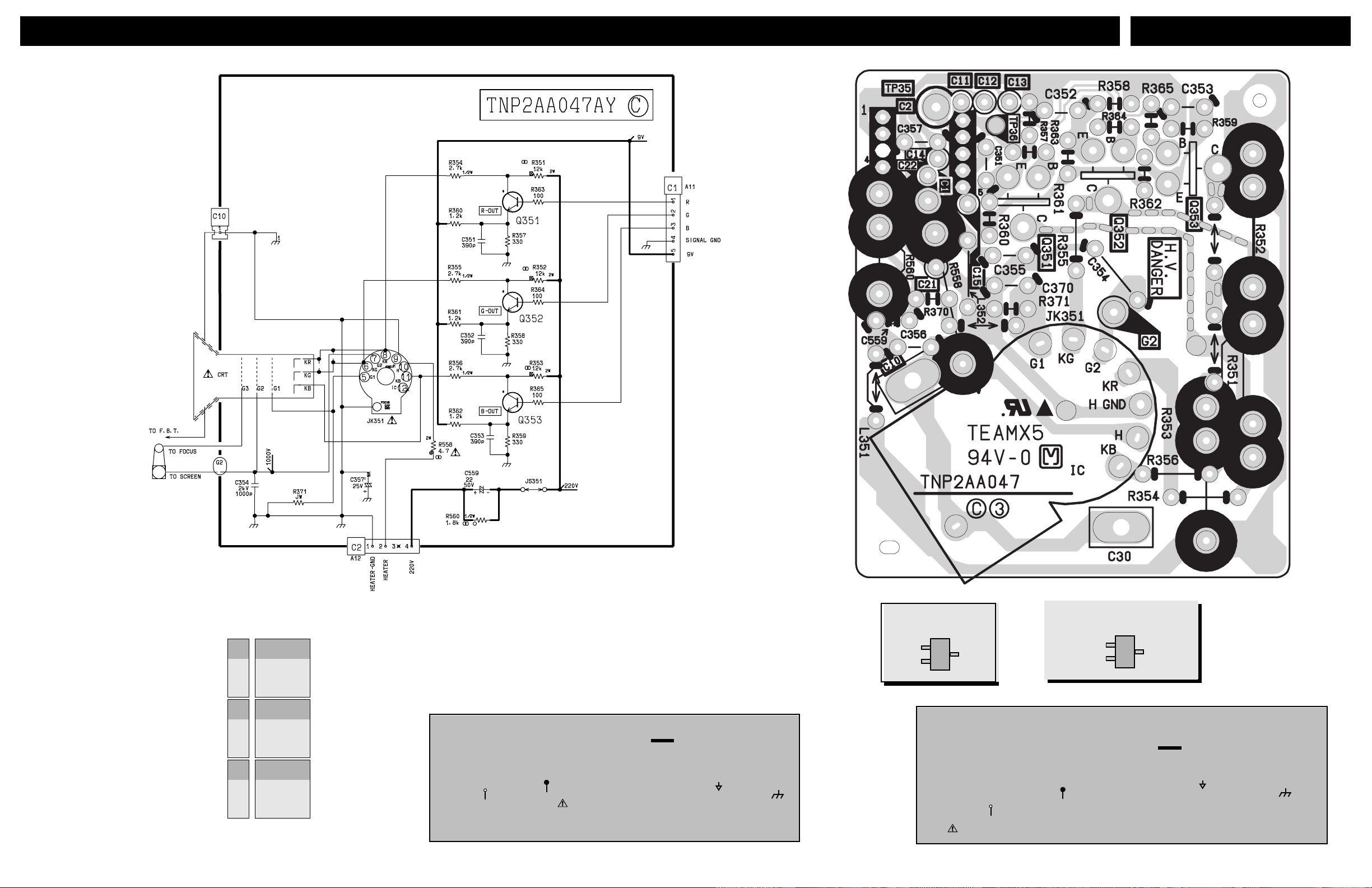
C-BOARD SCHEMATIC,LAYOUT & VOLTAGES--DIAGRAMA ELECTRICO Y VOLTAJES TARJETA C
ALL MODELS
CHIP TRANSISTOR
LEAD DESIGNATION
Q351
B
C
E
3.23
136.29
3.00
Nota:
La medición de los voltajes se
hizo con un Voltímetro Digital.
Note:
Obtained voltages with a
multimeter.
B
E
C
Q352
B
C
E
B
C
E
3.30
133.16
3.00
Q353
3.34
132.8
3.00
1. Resistors are carbon 1/4W unless noted
otherwise.
2. Capacitors are ceramic 50V unless noted
otherwise.
3. Coil value notes is inductance in µH.
4. Test point indicated by ; Test point but
no pin .
5. Components indicated with are critical
parts and replacement should be made
with manufacture specified replacement
parts only.
Schematic Notes
6. (BOLD LINE) indicates the
route of B+ supply.
7. The schematic diagrams are current at
the time of printing and are subject to
change without notice.
8. Ground symbol indicates HOT
GROUND CONNECTION;
indicates COLD GROUND.
NOTE: All other component symbols are
used for engineering design
purposes.
1. Las Resistencias son de Carbón de 1/4W, a
menos que se indique otra característica.
2. Los Capacitores son de Cerámica para 50V, a
menos que se indique otra característica.
3. El valor indicado de las Bobinas es la
inductancia expresada en µH.
4. Los puntos de prueba en la terminal de algún
componente son indicados por Los puntos
de prueba fuera de los componentes se
indican con .
5. Los componentes señalados con el símbolo
son considerados componentes críticos y
IDENTIFICACIÓN DE TERMINALES
PARA TRANSISTORES EN
B
E
Notas de los Diagramas
CHIP
C
deben ser reemplazados sólo con las partes
especificadas por el fabricante.
6. (LINEA GRUESA) indica las líneas de
alimentación de los Voltajes B+.
7. Los diagramas eléctricos están sujetos a
cambio sin previo aviso.
8. El símbolo indica que es una conexión a
Tierra Caliente y el símbolo indica
conexión a Tierra Fría.
NOTA: Los demas símbolos de componentes
incluidos son usados con fines de
diseño.
- 38 -
Page 38
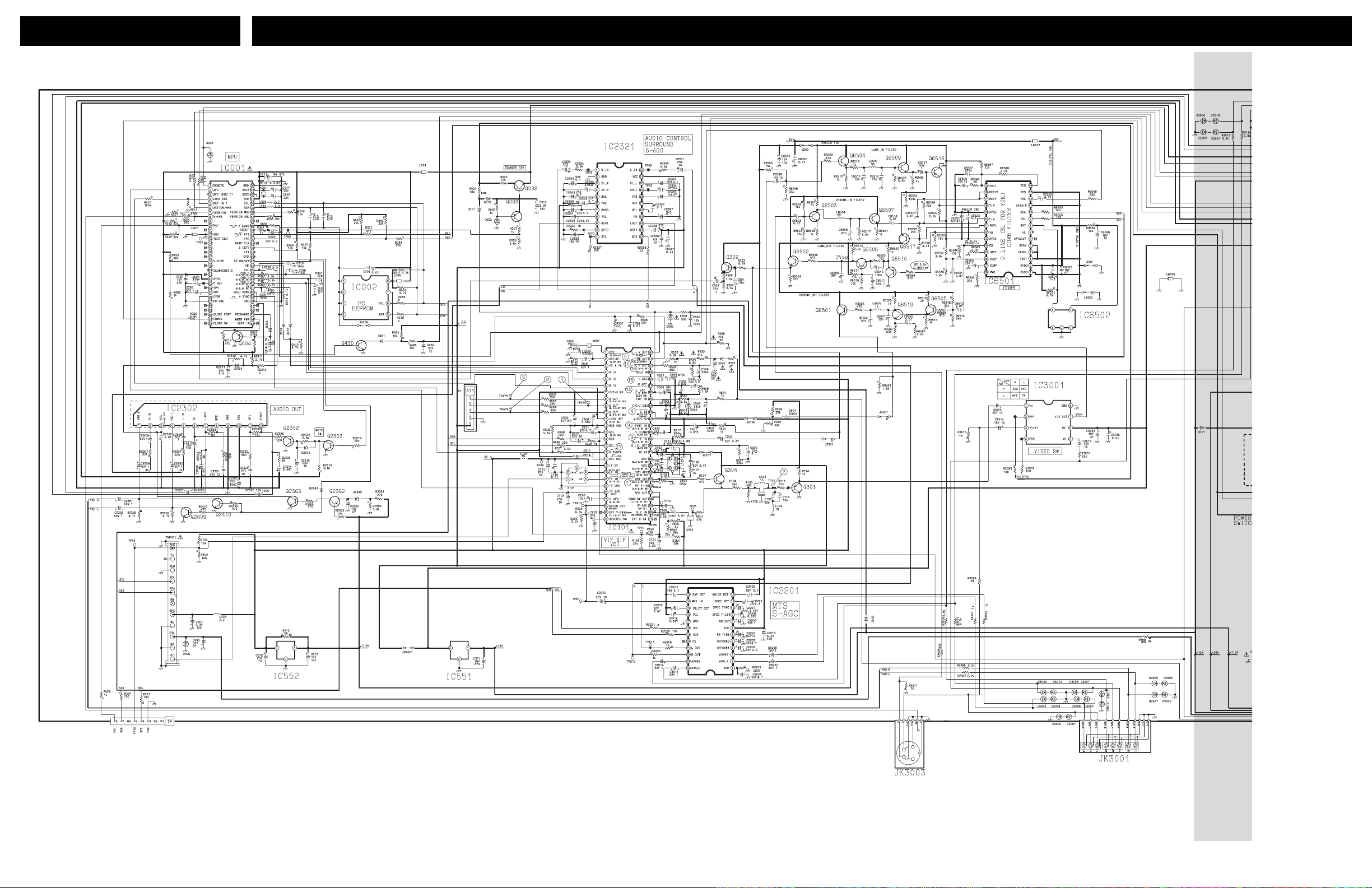
ALL MODELS
A-BOARD SCHEMATIC LEFT PORTION -- DIAGRAMA ELECTRICO DE LA TARJETA A, SECCION IZQUIERDA
- 39 -
Page 39
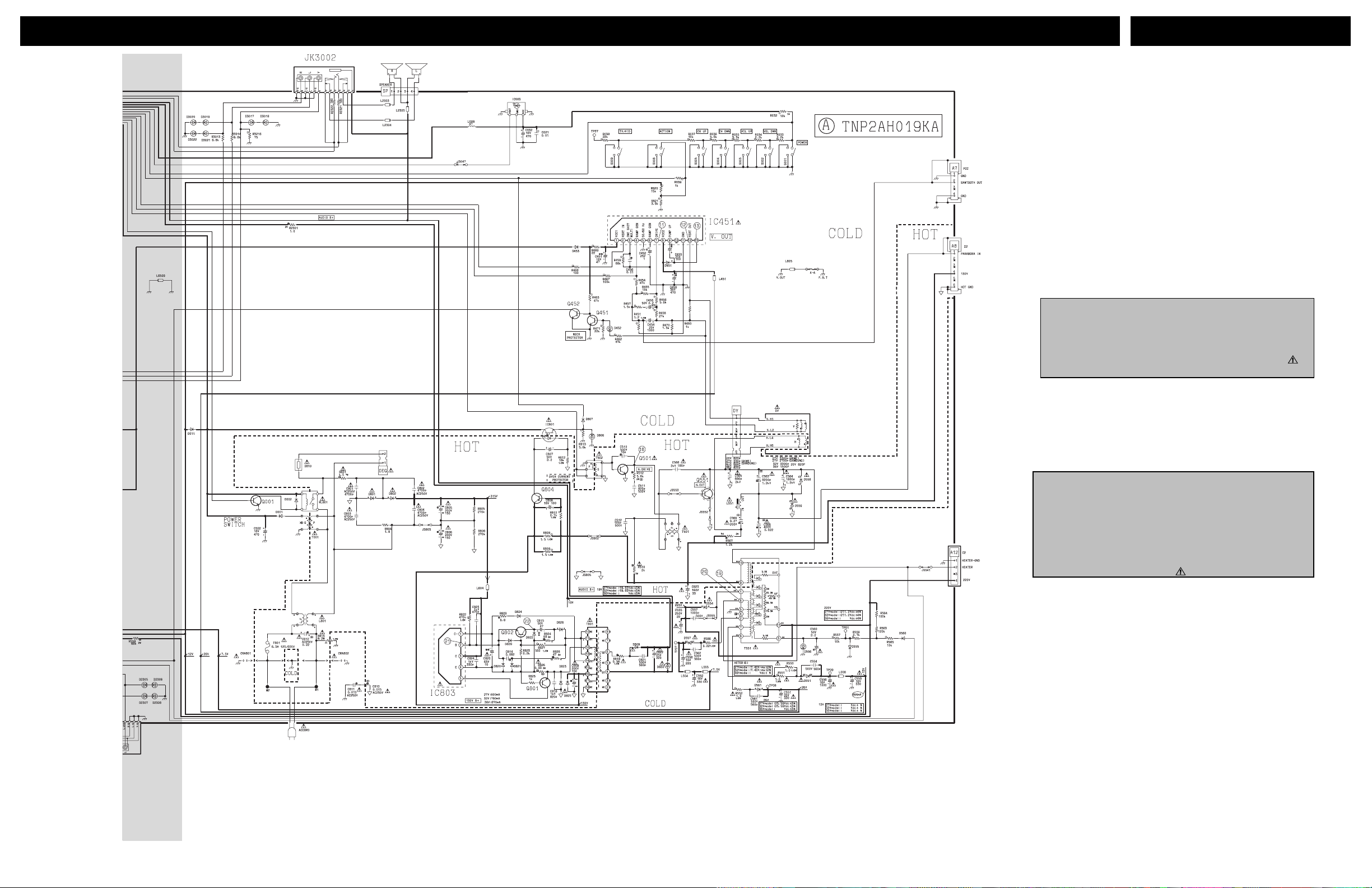
A-BOARD SCHEMATIC RIGHT PORTION -- DIAGRAMA ELECTRICO TARJETA A SECCION DERECHA
ALL MODELS
IMPORTANT SAFETY NOTICE
THIS SCHEMATIC DIAGRAM INCORPORATES SPECIAL FEATURES
THAT ARE IMPORTANT FOR PROTECTION FROM X-RADIATION, FIRE
AND ELECTRICAL SHOCK HAZARDS. WHEN SERVICING IT IS
ESSENTIAL THAT ONLY MANUFACTURERS SPECIFIED PARTS BE
USED FOR THE CRITICAL COMPONENTS DESIGNATED WITH A IN
THE SCHEMATIC.
NOTA DE SEGURIDAD
LOS DIAGRAMAS ELÉCTRICOS INCLUYEN CA RACTERÍSTICAS
ESPECIALES MUY IMPORTANTES PARA LA PROTECCIÓN
CONTRA RAYOS-X, QUEMADURAS Y DESCARGAS
ELÉCTRICAS. CUANDO SE DE SERVICIO ES IMPORTANTE
USAR PARA REEMPLAZO DE COMPONENTES CRITICOS,
SOLO PARTES ESPECIFICADAS POR EL FABRICANTES. LOS
COMPONENTES CRITICOS ESTAN SEÑALADOS EN LOS
DIAGRAMAS POR EL SIMBOLO
.
- 40 -
Page 40
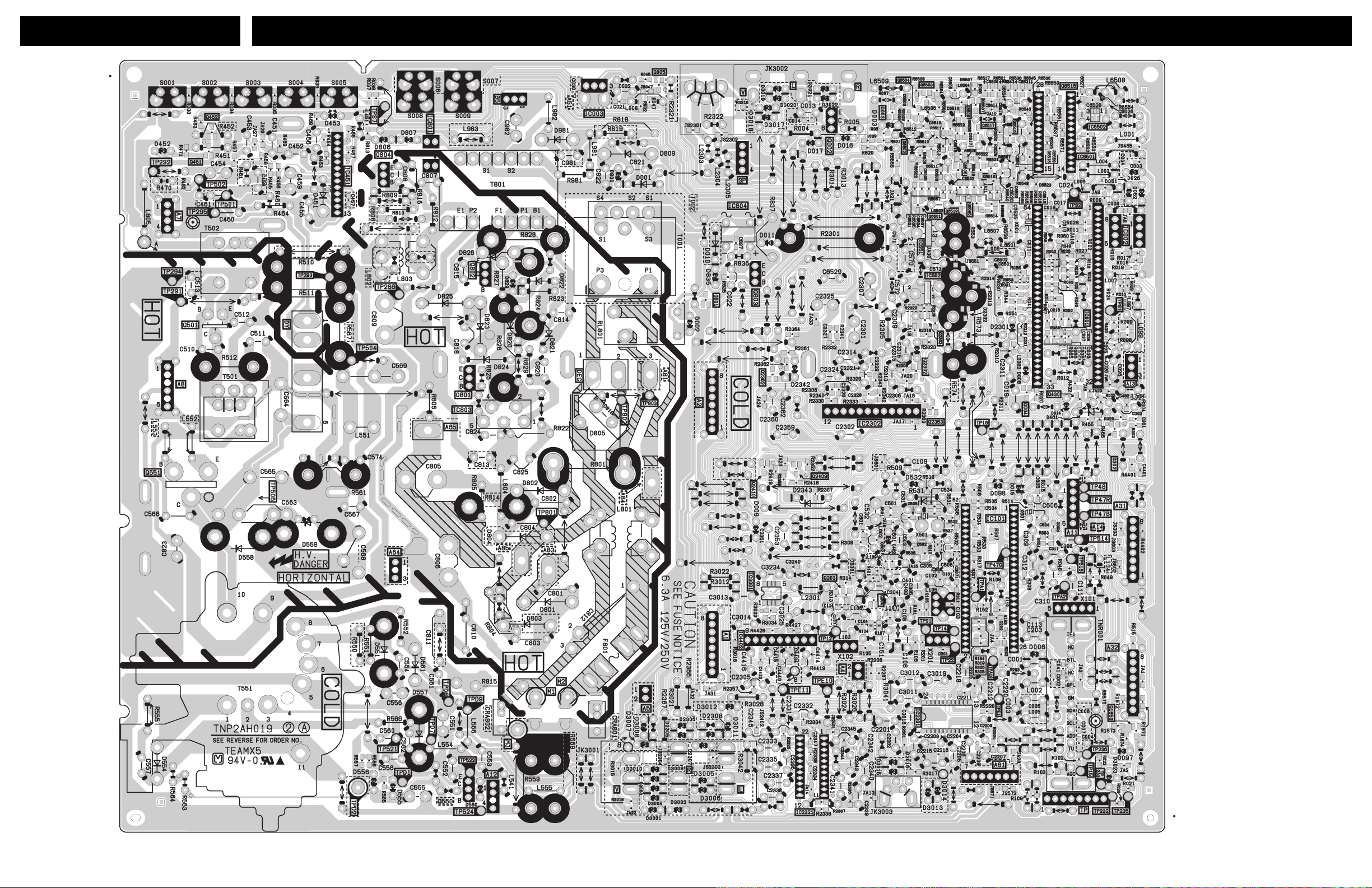
ALL MODELS
A-BOARD LAYOUT -- DIAGRAMA IMPRESO DE LA TARJETA A
- 41 -
Page 41
VOLTAGES A-BOARD -- VOLTAJES TARJETA A
ALL MODELS
1
. . . . . .4.40
. . . . . .2.53
2
. . . . . .0.00
3
. . . . . .3.43
4
. . . . . .5.17
5
. . . . . .2.73
6
. . . . . .0.00
7
. . . . . .5.17
8
. . . . . .0.00
9
. . . . . .5.17
10
. . . . . .0.00
11
. . . . . .0.0
12
. . . . . .2.59
13
. . . . . .0.00
14
. . . . . .0.00
15
. . . . . .0.00
16
. . . . . .0.00
17
. . . . . .0.42
18
. . . . . .0.00
19
. . . . . .0.00
20
. . . . . .0.00
21
. . . . . .5.18
22
. . . . . .0.00
23
. . . . . .1.92
24
. . . . . .1.28
25
. . . . . .1.86
26
. . . . . .0.00
27
. . . . . .0.00
28
. . . . . .0.00
29
. . . . . .0.00
30
. . . . . .5.13
31
. . . . . .0.00
32
IC002
1
. . . . . . 0.00
2
. . . . . . 0.00
3
. . . . . . 0.00
4
. . . . . . 0.00
5
. . . . . . 3.14
6
. . . . . . 3.16
7
. . . . . . 0.00
8
. . . . . . 5.18
IC003
1
. . . . . . 4.43
2
. . . . . . 0.00
3
. . . . . . 5.18
IC001
33
. . . . . .0.00
34
. . . . . .5.16
35
. . . . . .5.18
36
. . . . . .0.00
37
. . . . . .0.00
38
. . . . . .0.00
39
. . . . . .0.15
40
. . . . . .4.15
41
. . . . . .0.00
42
. . . . . .0.00
43
. . . . . .0.00
44
. . . . . .0.00
45
. . . . . .0.26
46
. . . . . .0.00
47
. . . . . .0.00
48
. . . . . .0.00
49
. . . . . .0.00
50
. . . . . .0.00
51
. . . . . .0.00
52
. . . . . .0.00
53
. . . . . .0.00
54
. . . . . .5.10
55
. . . . . .4.10
56
. . . . . .0.00
57
. . . . . .0.00
58
. . . . . .5.17
59
. . . . . .3.12
60
. . . . . .3.18
61
. . . . . .5.18
62
. . . . . .2.34
63
. . . . . .2.18
64
. . . . . .0.00
IC2321
1
. . . . . 4.44
2
. . . . . 0.00
3
. . . . . 4.47
4
. . . . . 4.46
5
. . . . . 4.48
6
. . . . . 4.43
7
. . . . . 4.53
8
. . . . . 5.54
9
. . . . . 4.44
10
. . . . . 1.52
11
. . . . . 3.15
12
. . . . . 3.13
13
. . . . . 5.57
14
. . . . . 4.46
15
. . . . . 4.44
16
. . . . . 4.43
17
. . . . . 4.46
18
. . . . . 4.44
19
. . . . . 4.46
20
. . . . . 4.47
21
. . . . . 8.95
22
. . . . . 4.44
IC2201
1
. . . . . 1.20
2
. . . . . 2.18
3
. . . . . 2.18
4
. . . . . 2.30
5
. . . . . 2.18
6
. . . . . 0.28
7
. . . . . 4.94
8
. . . . . 2.33
9
. . . . . 2.43
10
. . . . . 0.40
11
. . . . . 2.24
12
. . . . . 3.11
13
. . . . . 3.34
14
. . . . . 2.18
15
. . . . . 3.38
16
. . . . . 3.47
17
. . . . . 0.00
18
. . . . . 3.16
19
. . . . . 3.12
20
. . . . . 0.00
21
. . . . . 2.24
22
. . . . . 2.22
23
. . . . . 2.18
24
. . . . . 2.18
IC2302
1
. . . . . 6.04
2
. . . . . 6.77
3
. . . . . 0.31
4
. . . . . 5.97
5
. . . . . 6.78
6
. . . . 18.60
7
. . . . 11.18
8
. . . . 11.32
9
. . . . . 0.00
10
. . . . 24.33
11
. . . . 11.37
12
. . . . 11.20
1
. . . . . 2.80
2
. . . . . 5.64
3
. . . . . 0.00
4
. . . . . 0.00
5
. . . . . 0.00
6
. . . . . 0.00
7
. . . . . 8.95
8
. . . . . 3.24
9
. . . . . 3.29
10
. . . . . 3.28
11
. . . . . 4.20
12
. . . . . 0.00
13
. . . . . 3.36
14
. . . . . 3.14
15
. . . . . 3.18
16
. . . . . 0.00
17
. . . . . 3.50
18
. . . . . 4.91
19
. . . . . 2..71
20
. . . . . 2.71
21
. . . . . 0.00
22
. . . . . 1.62
23
. . . . . 5.10
24
. . . . . 4.09
25
. . . . 17.81
26
. . . . . 5.75
IC3001
1
. . . . . .4.04
2
. . . . . .0.00
3
. . . . . .4.05
4
. . . . . .0.00
5
. . . . . .4.05
6
. . . . . .8.96
7
. . . . . .4.28
8
. . . . . .0.00
IC551
1
. . . . .13.14
2
. . . . . .0.00
3
. . . . . .8.97
IC804
1
. . . . .13.50
2
. . . . . .0.00
3
. . . . . .6.40
4
. . . . . .6.27
IC101
27
. . . . . 4.93
28
. . . . . 3.17
29
. . . . . 2.61
30
. . . . . 2.22
31
. . . . . 4.66
32
. . . . . 1.77
33
. . . . . 2.98
34
. . . . . 2.60
35
. . . . . 3.42
36
. . . . . 3.42
37
. . . . . 8.96
38
. . . . . 3.99
39
. . . . . 4.37
40
. . . . . 2.82
41
. . . . . 4.44
42
. . . . . 4.49
43
. . . . . 3.58
44
. . . . . 0.00
45
. . . . . 0.47
46
. . . . . 6.03
47
. . . . . 4.01
48
. . . . . 2.09
49
. . . . . 5.30
50
. . . . . 0.86
51
. . . . . 6.01
52
. . . . . 4.11
IC451
1
. . . . . 8.22
2
. . . . . 4.11
3
. . . . . 4.12
4
. . . . . 4.16
5
. . . . . 0.00
6
. . . . . 3.93
7
. . . . . 3.99
8
. . . . 24.64
9
. . . . . 1.51
10
. . . . . 1.37
11
. . . . . 0.00
12
. . . . 12.79
13
. . . . 24.81
IC552
1
. . . . . 8.44
2
. . . . . 0.00
3
. . . . . 4.96
IC6501
1
. . . . . .0.00
2
. . . . . .4.96
3
. . . . . .0.00
4
. . . . . .0.00
5
. . . . . .0.00
6
. . . . . .0.00
7
. . . . . .0.00
8
. . . . . .4.95
9
. . . . . .3.18
10
. . . . . .3.15
11
. . . . . .0.00
12
. . . . . .2.41
13
. . . . . .0.00
14
. . . . . .2.32
15
. . . . . .2.47
16
. . . . . .3.46
17
. . . . . .3.46
18
. . . . . .2.35
19
. . . . . .0.00
20
. . . . . .2.46
21
. . . . . .1.47
22
. . . . . .0.50
23
. . . . . .4.95
24
. . . . . .0.38
25
. . . . . .1.14
26
. . . . . .1.13
27
. . . . . .3.58
28
. . . . . .0.57
IC6502
1
. . . . . .0.00
2
. . . . . .0.00
3
. . . . . .0.00
4
. . . . . .4.95
5
. . . . . .4.93
IC801
1
. . . . . .0.59
2
. . . . . .0.00
3
. . . . .12.27
4
. . . . . .0.00
IC803
1
. . . . .90.12
2
. . . .132.14
3
. . . .249.21
4
. . . .131.90
5
. . . .133.2
Q001
B
C
E
0.75
0.00
0.00
Q2303
B
C
E
0.00
24.32
0.00
Q302
B
C
E
2.55
4.95
1.95
Q452
B
C
E
0.00
3.60
0.00
Q6503
B
C
E
2.40
2.71
1.79
Q6509
B
C
E
2.27
4.95
1.64
Q801
132.10
B
133.00
C
132.20
E
Q002
5.86
10.14
5.18
Q2362
8.45
0.00
7.90
Q303
1.20
0.00
1.88
Q501
0.00
82.70
0.00
Q6504
3.30
5.00
2.70
Q6510
0.43
0.00
1.10
Q802
129.40
133.00
133.10
Q003
5.01
5.83
5.83
Q2363
0.00
0.30
0.00
Q304
2.42
8.96
1.85
Q551
0.00
17.00
0.00
Q6505
2.38
4.96
1.76
Q6516
1.73
0.00
2.36
Q803
12.00
13.60
12.30
Q004
4.89
0.00
5.16
Q2409
0.00
0.00
0.00
Q430
0.28
4.02
0.00
Q6501
3.30
4.96
2.68
Q6506
2.25
3.24
1.65
Q6517
1.46
4.96
1.73
Q804
131.90
0.59
132.30
Q2302
24.30
0.00
18.60
Q2410
0.00
0.00
0.00
Q451
0.62
0.00
0.00
Q6502
3.23
4.96
2.57
Q6507
2.71
4.95
2.08
Q6519
1.76
3.31
1.13
IDENTIFICACIÓN DE TERMINALES
PARA TRANSISTORES EN
B
E
CHIP TRANSISTOR
LEAD DESIGNATION
B
E
CHIP
C
C
Voltage Measurements
1. Voltage measurement:
- AC input to the Receiver is 120V.
NTSC (HD, 1125i & 525P when
applicable) signal generator is
connected to the antenna of the
Receiver. (Color bar pattern of
100 IRE white and 7.5 IRE black.)
- All Picture and Audio a djust men ts
are set to Normalize.
TV ANT/CABLE - (Set-Up Menu)
in TV/ANT Mode
Volume - Min.
TV/Video SW - TV position
Audio Mode - Stereo
- Voltage readings are nominal
and may vary ±10% on active
devices. Some voltage
reading will vary with signal
strength and picture content.
- Supply voltages are nominal.
2. Ground symbol indicates
ground lead connection of meter.
Incorrect ground connection will
result in erroneous readings.
CAUTION: Incorrect ground
connection of the test equipment
will result in erroneous readings.
- 42 -
Page 42
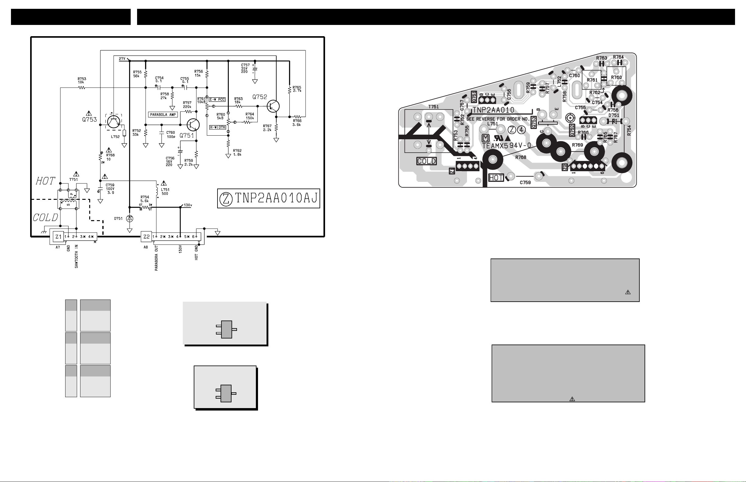
ALL MODELS
Z-BOARD SCHEMATIC,LAYOUT & V OLTAGES -- DIAGRAMA ELECTRICO,CIRCUITO IMPRESO Y VOLTAJES TARJETA Z
IMPORTANT SAFETY NOTICE
THIS SCHEMATIC DIAGRAM INCORPORATES SPECIAL FEATURES
THAT ARE IMPORTANT FOR PROTECTION FROM X-RADIATION, FIRE
AND ELECTRICAL SHOCK HAZARDS. WHEN SERVICING IT IS
ESSENTIAL THAT ONLY MANUFACTURERS SPECIFIED PARTS BE
USED FOR THE CRITICAL COMPONENTS DESIGNATED WITH A IN
THE SCHEMATIC.
Q751
B
C
E
0.00
11.52
0.00
Q752
B
C
E
10.52
0.00
11.01
Q753
B
C
E
0.60
8.06
0.00
IDENTIFICACIÓN DE TERMINALES
PARA TRANSISTORES EN
B
E
CHIP TRANSISTOR
LEAD DESIGNATION
B
E
CHIP
C
C
Nota:
La medición de los voltajes se
hizo con un Voltímetro Digital.
Note:
Obtained voltages with a digital
multimeter.
NOTA DE SEGURIDAD
LOS DIAGRAMAS ELÉCTRICOS INCLUYEN CARACTERÍSTICAS
ESPECIALES MUY IMPORTANTES PARA LA PROTECCIÓN
CONTRA RAYOS-X, QUEMADURAS Y DESCARGAS
ELÉCTRICAS. CUANDO SE DE SERVICIO ES IMPORTANTE
USAR PARA REEMPLAZO DE COMPONENTES CRITICOS,
SOLO PARTES ESPECIFICADAS POR EL FABRICANTES. LOS
COMPONENTES CRITICOS ESTAN SEÑALADOS EN LOS
DIAGRAMAS POR EL SIMBOLO
.
- 43 -
Page 43
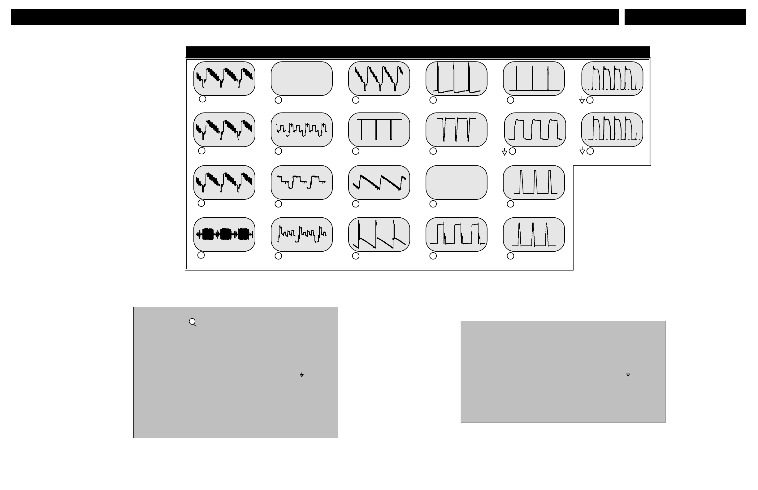
WAVEFORMS A-BOARD -- FORMAS DE ONDA TARJETA A
Waveforms - A-Board
3.58MHz X’tal
ALL MODELS
2.0V p-p [20µs]
1
IC101 PIN 33 (DET OUT)
1.0V p-p [20µs]
2
3
4
TP12
2.0V p-p [20µs]
IC101 PIN 39 (Y IN)
0.4V p-p [20µs]
IC101 PIN 43 (C IN)
IC101 PIN 1
5
OSC Waveform
4.7V p-p [20µs]
6
4.1V p-p [20µs]
7
4.3V p-p [20µs]
8
A11 PIN 3 (B)
3.58VCO
A11 PIN 1 (R)
TP47R
A11 PIN 2 (G)
TP47G
TP47B
1.5-1.9V p-p [20µs]
9
IC101 PIN 41 (SYNC)
4.2V p-p [5ms]
10
IC101 PIN 52 (VERT OUT)
1.7V p-p [5ms]
11
IC451 PIN 7 (DRIVE)
55.1V p-p [5ms]
12
IC451 PIN 12 (VERT OUT)
30.8V p-p [5ms]
13
IC451 PIN 13
0.14V p-p [20µs]
14
IC101 PIN 47 ( H A FC)
503KHz X’tal
IC101 PIN 48
15
16
H OSC
OSC Waveform
3.4-4.0V p-p [20µs]
IC101 PIN 50 (H OUT)
7.5V p-p [20µs]
17
IC101 PIN 16 (H SYNC)
175.1V p-p [20µs]
18
Q501 collector (H DRI VE)
259.3V p-p [20µs]
19
T551 PIN 1
24.4-27.2V p-p [20µs]
20
T551 PIN 6
326.9V p-p [5µs]
21
IC803 PIN 2
325.0V p-p [5µs]
22
Collector of Q802
Medición de Formas de Onda
1. Un símbolo como indica el punto
para medir una señal. (La medic ión
puede hacerse en el punto con
mayor accesibilidad, siempre que
sea común al indicado.)
2. Se midieron utilizando un
generador con formato NTSC
conectado a la terminal de la
antena. (Patrón de 8 Barras de
Colores EAI, formato NTSC de 100
IREs para el Blanco y 7.5 IREs
para el Negro.)
3. Los ajustes de usuario de los
Menus PICTURE y AUDIO se
normalizaron. Posteriormente el
nivel de volumen se ajusta al
mínimo.
3
4. Las formas de onda de Video y
Color fueron tomadas con un
osciloscopio de banda alta y con un
punta de prueba de baja
capacitancia (10 a 1). La forma y
amplitud de las ondas puede variar
según el tipo de osciloscopio que
se utilice y sus características.
5. El símbolo de tierra que aparece
junto al número de la forma de
onda, indica que se utiliza conexión
a Tierra Caliente en el extremo
negativo de la punta de prueba.
PRECAUCION: Si no se utiliza la
conexión a la tierra adecuada, se
obtendrán mediciones equivocadas
y podría dañar el equipo de
medición.
- 44 -
Voltage Measurements
1. Voltage measurement:
- AC input to the Receiver is 120V.
NTSC (HD, 1125i & 525P when
applicable) signal generator is
connected to the antenna of the
Receiver. (Color bar pattern of
100 IRE white and 7.5 IRE black.)
- All Picture and Audio a djust men ts
are set to Normalize.
TV ANT/CABLE - (Set-Up Menu)
in TV/ANT Mode
Volume - Min.
TV/Video SW - TV position
Audio Mode - Stereo
- Voltage readings are nominal
and may vary ±10% on active
devices. Some voltage
reading will vary with signal
strength and picture content.
- Supply voltages are nominal.
2. Ground symbol indicates
ground lead connection of meter.
Incorrect ground connection will
result in erroneous readings.
CAUTION: Incorrect ground
connection of the test equipment
will result in erroneous readings.
Page 44

- 45 -
Page 45
PARTS LIST ABBREVIATIONS GUIDE
RESISTOR
TYPE TOLERANCE
CCarbonF ± 1%
FFuseJ± 5%
M Metal Oxide K± 10%
S Solid M± 20%
WWire WoundG± 2%
RES, C 270-J-1/4
CAPACITOR
TYPE TOLERANCE
C Ceramic C ± 0.25pF
E Electrolytic D ± 0.5pF
P Polyester F± 1pF
SStyrolJ± 5%
T Tantalum K± 10%
L± 15%
M± 20%
P +10% -0%
Z +80% -20%
CAP, P .068UF-K-50V
- 46 -
Page 46

®
- 47 -
Printed in USA
K01072593CM0718
 Loading...