

Specification*
ORDER No. ACED030757C3
AUTOMOTIVE AFTERMARKET
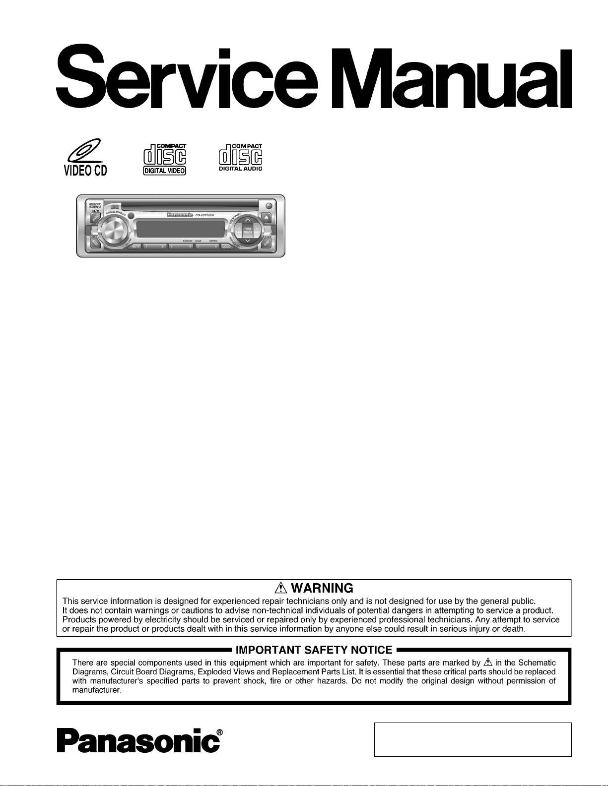
CQ-VCD163WJ
Removable Front Panel Video CD
Player / Receiver
General
Power Supply DC 12V (11V - 16V),
Test Voltage 14.4V
Negative Ground
Tone Controls Bass ; ±12dB at 100Hz
Treble ; ±12dB at 10kHz
Current Consumption Less than 2.2A (CD play mode,
0.5W×4ch)
Maximum Power Output 50W×4ch (at 1kHz, Vol. Max.)
Suitable Speaker Impedance 4-8Ω
Pre-Amp Output Voltage 2.5V (VCD play mode; 1kHz, 0dB)
Output Impedance 200Ω
FM Stereo Radio
Frequency Range 87.5 - 108MHz
Usable Sensitivity 11.0dBf (1.25µV, 75Ω)
AM Radio
Frequency Range 531 - 1,602kHz
Usable Sensitivity 28dB/µV (25µV, S/N 20dB)
CD / Video CD Player
Sampling Frequency 32 times oversampling
Pick-Up Type Astigma 3-beam
Light Source Semiconductor Laser
Wavelength 780nm
Frequency Response 5Hz to 20,000Hz (±1dB)
Signal to Noise Ratio 96dB
Total Harmonic Distortion 0.006% (at 1kHz)
Wow and Flutter Below measurable limits
Video Signal Output Composite Video Signal, 1.0V[p-p]
75Ω
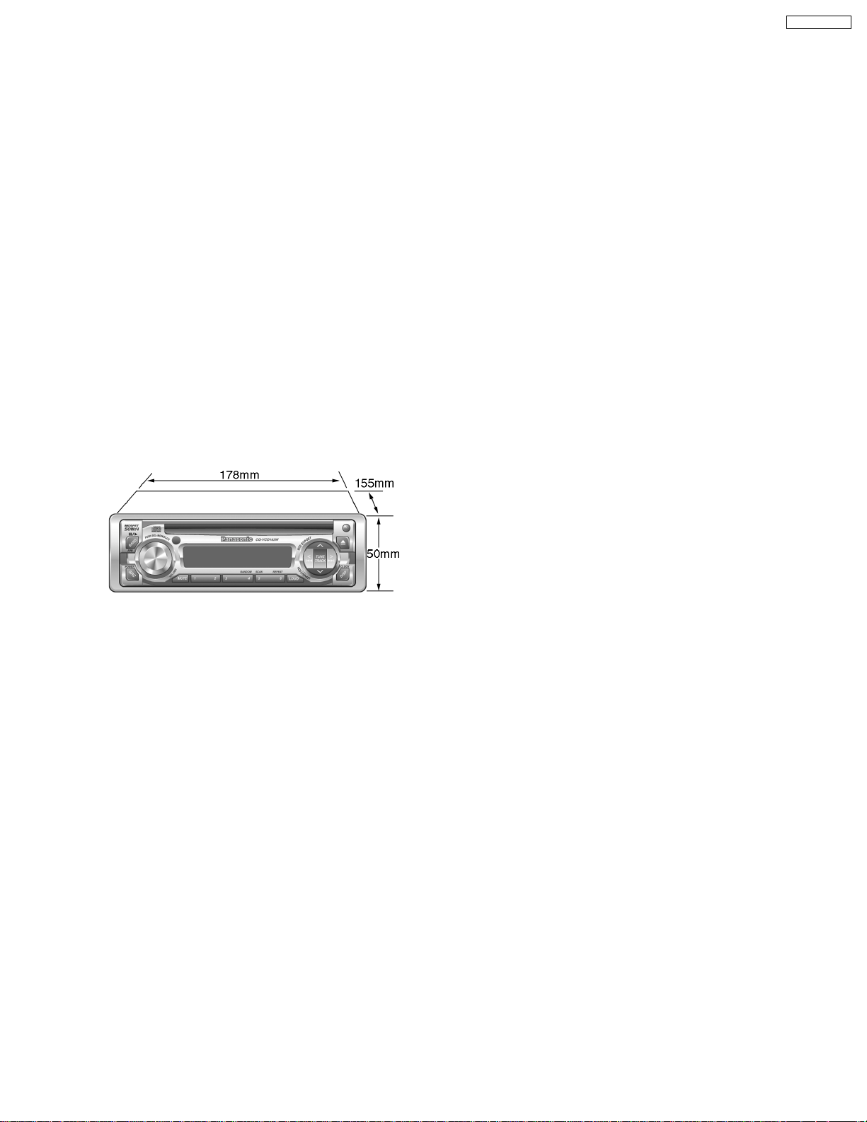
Dimensions** 178×50×155mm
Weight** 1.4kg
* Specifications and the design are subject to possible modification
without notice due to improvements.
** Dimensions and Weight shown are approximate.
© 2003 Matsushita Electric Industrial Co., Ltd. All
rights reserved. Unauthorized copying and
distribution is a violation of law.
CQ-VCD163WJ
CONTENTS
Page Page
1 FEATUERS 2
2 LASER PRODUCTS
3 REPLACEING THE FUSE
4 MAINTENANCE
5 NOTES
6 DIMENSIONS
7 WIRING DIAGRAM
8 BLOCK DIAGRAM
8.1. Main / Key Block
8.2. CD Servo Block
9 TERMINALS DESCRIPTION
9.1. Main Block
9.2. Display Block
9.3. CD Servo Block
10 PACKAGE AND IC BLOCK DIAGRAM
10.1. Main Block
10.2. Display Block
12
2
3
3
3
3
4
5
5
6
7
7
7
7
9
9
10.3. Interface Block 12
10.4. CD Servo Block
11 REPLACEM ENT PARTS LIST
12 EXPLODED VIEW (Unit)
13 CD PLAYER MECHANICAL PARTS LIST
14 EXPLODED VIEW (CD Deck)
15 WIRING CONNECTION
15.1. Main Block-1
15.2. Main Block-2
15.3. Display Block
15.4. CD SERVO Block
16 SCHEMAT IC DIAGRAM-1
16.1. Main Block
17 SCHEMAT IC DIAGRAM-2
17.1. Display Block
17.2. CD Servo Block
17.3. Interface Block
13
14
20
21
22
23
23
24
25
26
27
27
29
29
30
31
1 FEATUERS
•
•
PLL (Phase Locked Loop) synthesized tuning.
• •
•
•
18-FM, 6-AM presets with preset scan
• •
•
•
Digital servo for reliable CD playback.
• •
•
•
Removable face plate.
• •
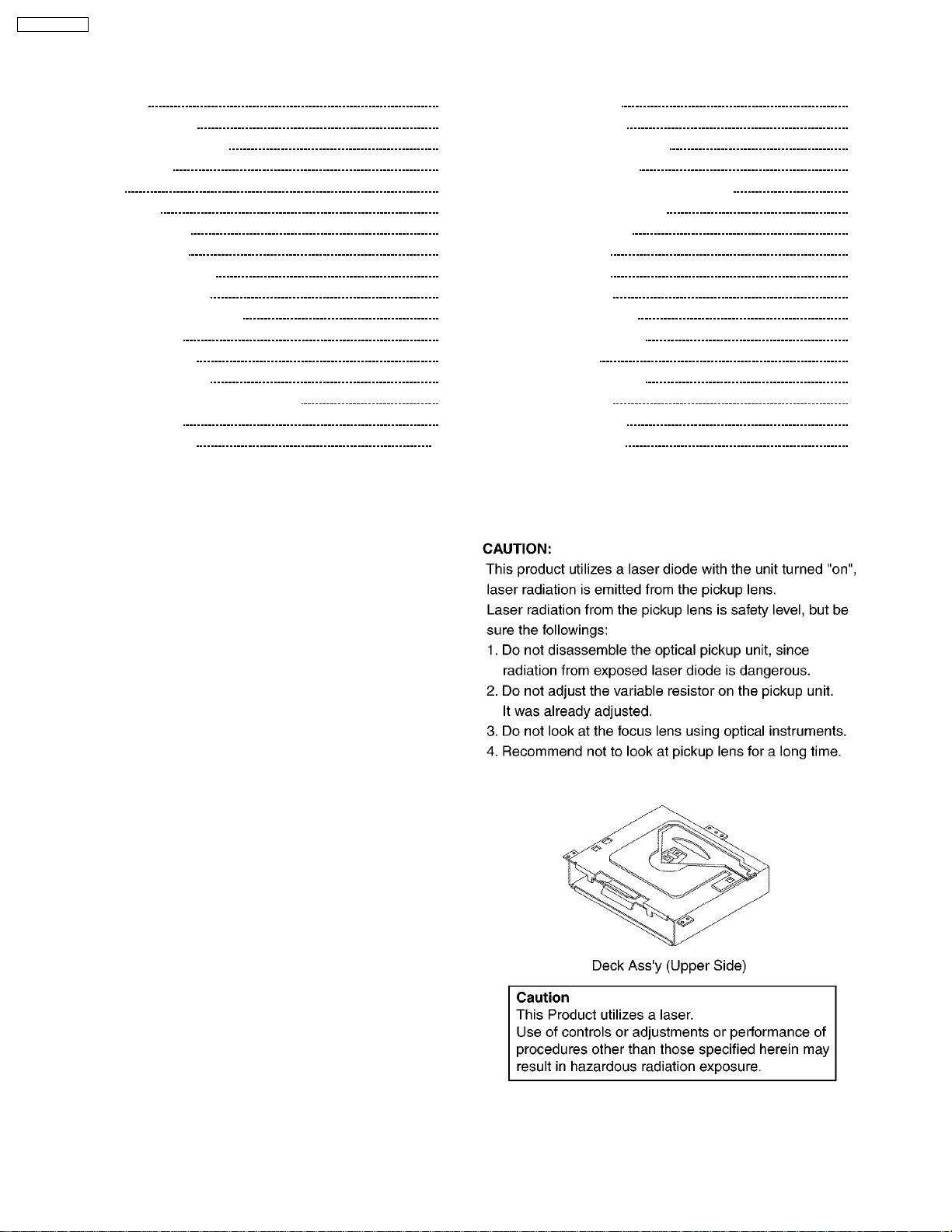
2 LASER PRODUCTS
2
3 REPLACEING THE FUSE
Use fuses of the same specified rating (15A). Using different
substitutes or fuses with higher ratings, or connecting the
product directly without a fuse, could cause fire or damage to
the stereo unit.
4 MAINTENANCE
Your products is designed and manufactured to ensure a
minimum of maintenance. Use a dry, a soft cloth for routine
exterior cleaning. Never use benzine, thinner or other solvents.
5 NOTES
[RADIO BLOCK]
Do not align the AM/FM package block. When the package
block is necessary, it will be supplied already aligned at the
factory.
[CD DECK BLOCK]
This model has no servo alignment points because
microcomputer controls the servo circuit.
CQ-VCD163WJ
6 DIMENSIONS
3
CQ-VCD163WJ
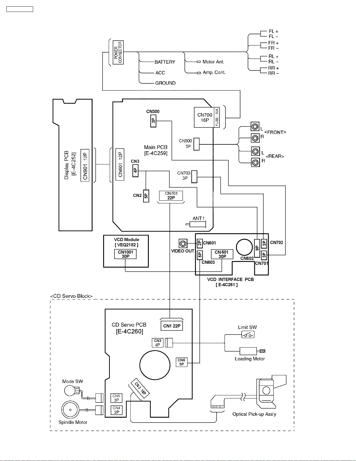
7 WIRING DIAGRAM
4
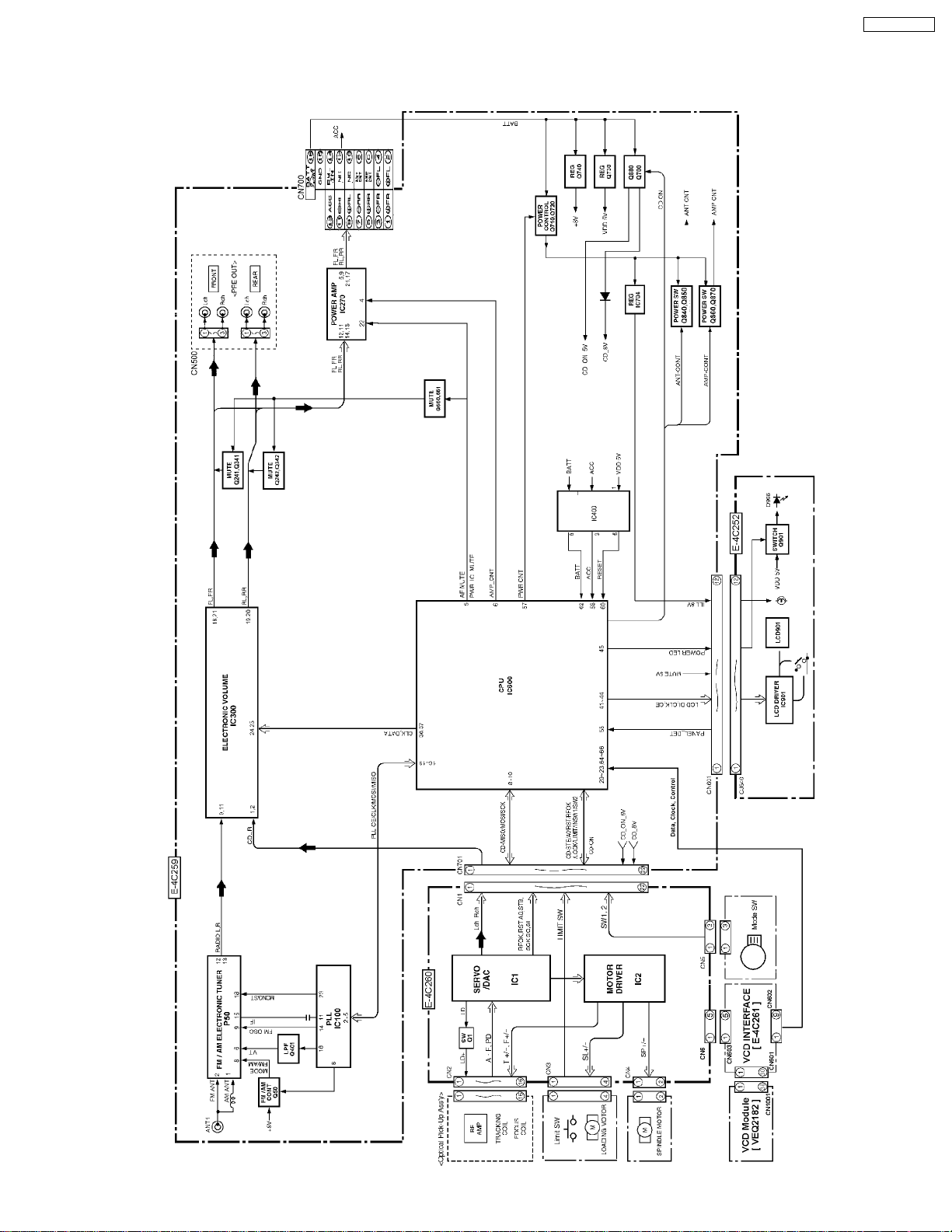
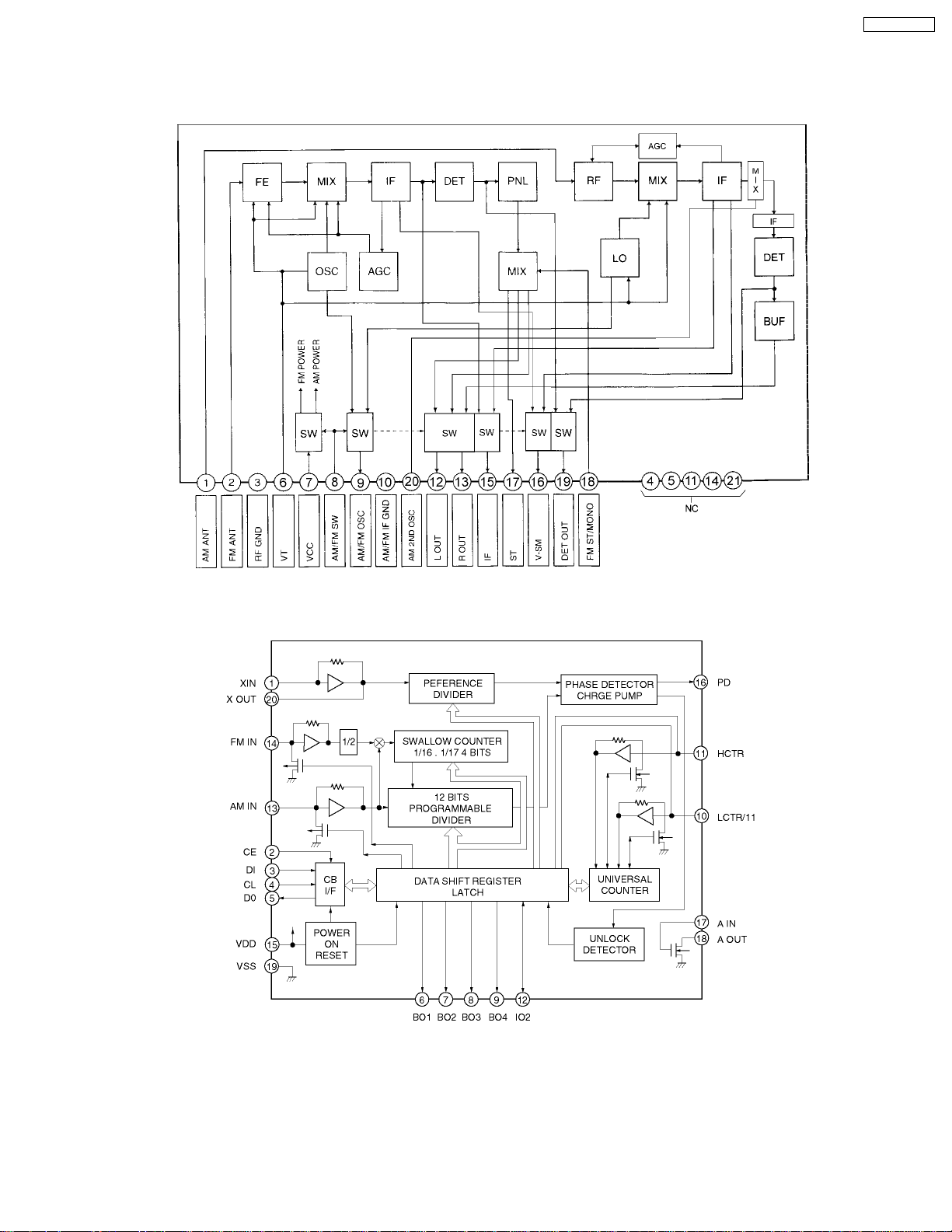
8 BLOCK DIAGRAM
8.1. Main / Key Block
CQ-VCD163WJ
5
CQ-VCD163WJ
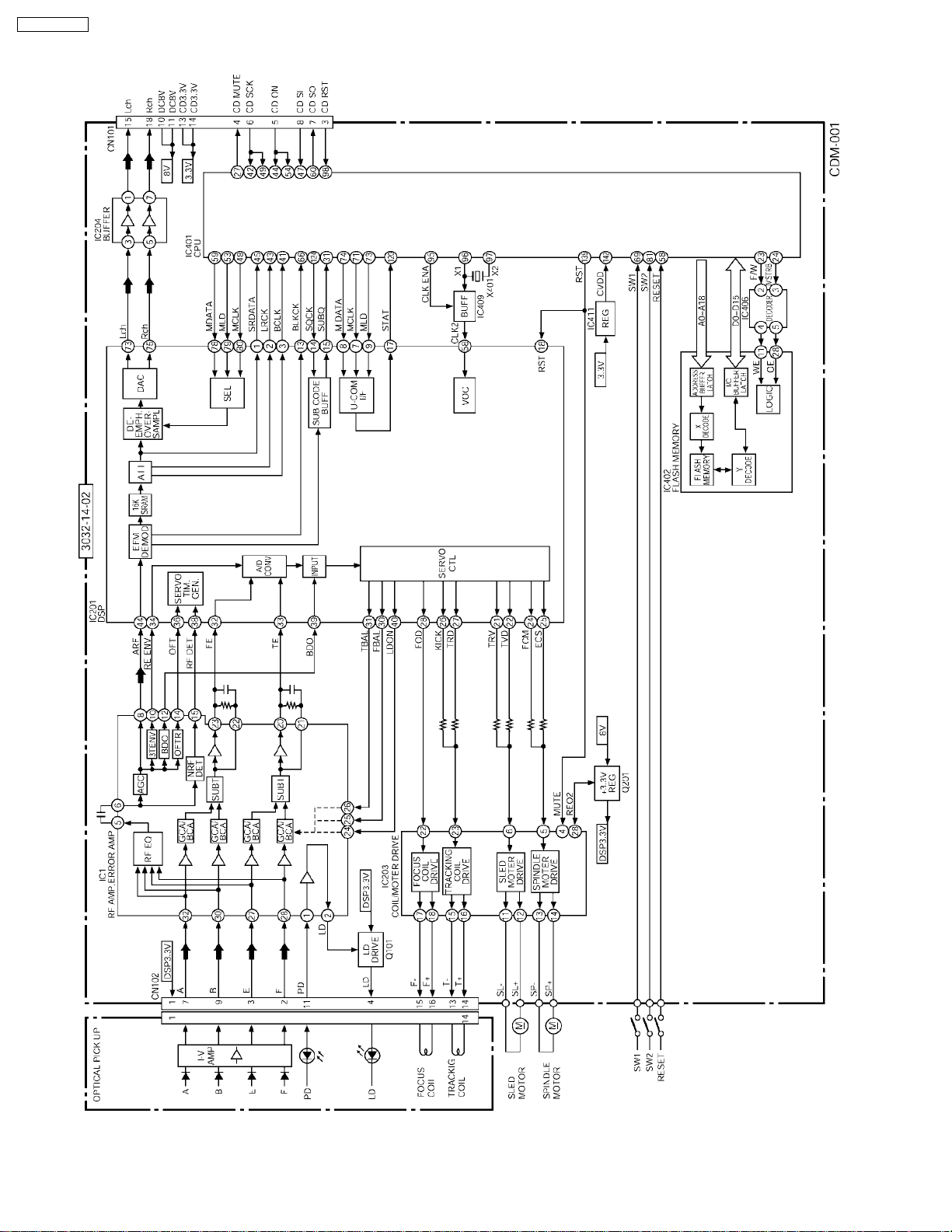
8.2. CD Servo Block
6
9 TERMINALS DESCRIPTION
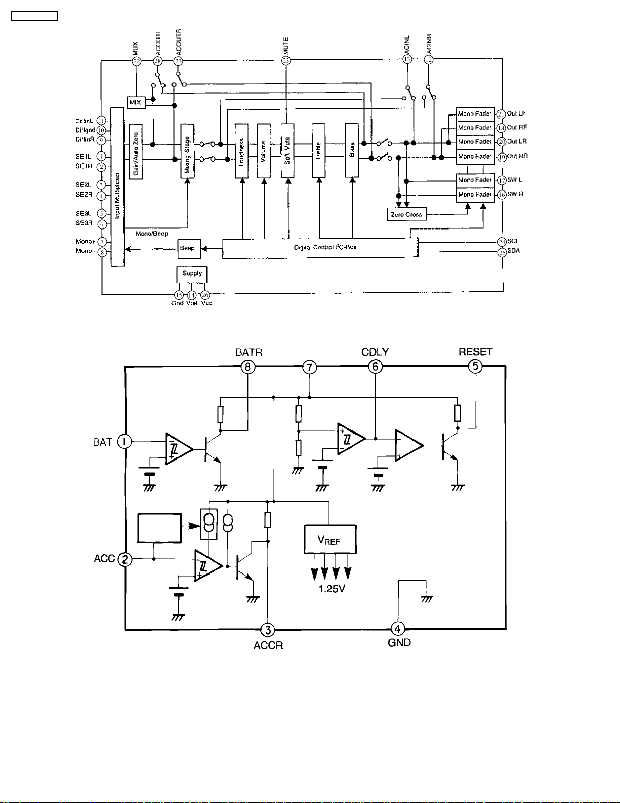
9.1. Main Block
CQ-VCD163WJ
IC600 : UPD784224116
Pin
No.
Port Descriptions I/O
1 NC (Connecting to ground) - 0 0 0
2 NC (Connecting to ground) - 0 0 0
3 NC (Connecting to ground) - 0 0 0
4 AVSS Analog ground - 0 0 0
5 AF MUTE AF mute O 5.1 5.1 5.2
6 AMP-CNT Power Amp. stand-by O 5.1 5.1 5.2
7 AVREF Reference voltage - 5.1 5.1 5.2
8 CD-MISO CD data I 0 0 0
9 CD-MOSI CD data O 0 0 2.4
10 CD-SCK CD clock O 0 0 5.1
11 NC Not used - - - 12 CD_OSCSTP CD OSC stop control I 0 0 0
13 NC Not used - - - 14 NC Not used - - - 15 VCD_CNT Video CD control O 0 0 5
16 PLL-MISO Data from PLL I 5.1 5.1 5.1
17 PLL-MOSI Data for PLL O 0 0 0
18 PLL-CLK Clock for PLL O 5.1 5.1 5.2
19 PLL-CE PLL chip enable O 0 0 0
20 HDIO Host serial data bus I/O 0 0 0
21 HCK Host Clock O 0 0 0
22 VRST Hardware reset O 0 0 0
23 HSEL Host address/data
24 CD-STB CD strobe O 0 0 5.1
25 CD-A0 CD address 0 O 0 0 4.4
26 CD-RST CD reset O 0 0 5.1
27 CD-RFOK CD RFOK signal I 0 0 5.0
28 CD-LOCK CD lock signal I 0 0 5.0
29 CD-LIMIT CD limit sw I 0 0 5.1
30 CD-SW2 CD SW2 I 5.1 5.1 0
31 MODE A MODE A I 5 5 5
32 MODE B MODE B I 5 5 0
33 Vss Ground - 0 0 0
34 NC Not used - - - 35 ST-IND FM stereo detection I 5.0 5.1 5.1
36 IC2-CLK Electronic volume clock O 5.1 5.1 5.2
37 IC2-DATA Electronic volume data I/O 5.1 0 5.2
38 NC No connection - - - 39 ILL8V LCD back light control I 5 5 5
40 NC No connection - - - 41 LCD-MOSI LCD data output O 0 0 0
42 LCD-MISO LCD data input I 5.0 5.0 5.0
43 LCD-CLK LCD clock O 0 0 0
44 LCD-CE LCD chip enable output O 0 0 0
45 POWER LED Pilot lamp on O 0 0 0
46 ANT.CONT Motor antenna control O 5.1 5.1 0
47 NC No connection - - - 48 EEPROM_SK Serial clock - - - 49 REM-IN_SUB Remote control sig.
50 EEPROM_DI EEPROM data input - - - 51 EEPROM_CS Chip select - - - 52 NC No connection - - - 53 EEPROM_DO EEPROM data output - - - 54 NC Not used - - - 55 PANEL-DET Panel detect I 0 4.8 4.9
56 CD-ON CD power control O 0 0 5.1
57 PWR CNT Power control O 5.0 5.0 5.0
58 ACC-DET ACC detection I 5.1 5.1 5.1
59 MUTE MUTE 0 5.1 5.1 5.1
60 /RESET Reset input I 5.1 5.1 5.1
61 REM Remocon data input I 4.4 4.4 4.4
62 BATT Battery detection I 5.1 5.1 5.1
63 CD SW1 CD SW1 I 0 0 0
64 DAC_MUTE DAC MUTE O 0 0 0
65 HRDY Host redy O 0 0 5
select
sampling
(V)FM(V)AM(V)CD(V)
O 0.6 0 0
I 0 4.4 4.4
Pin
No.
66 HINT Host interrupt I 0 0 5
67 VSS Ground - 0 0 0
68 VDD +5V power supply - 5.1 5.1 5.1
69 X2 Crystal oscillator - 3.1 3.1 3.1
70 X1 Crystal oscillator - 2.2 2.2 2.2
71 Vpp (Ground pull-down) - 0 0 0
72 SUB-X2 Crystal oscillator - 3.1 3.1 3.1
73 SUB-X1 Crystal oscillator - 2.5 2.5 2.5
74 AVDD +5V power supply - 5.1 5.1 5.1
75 AVREF (Connecting to VDD) - 5.1 5.1 5.1
76 VSM_DET S-meter detection I 0 0 0
77 NC Not used I 0 0 0
78 NC Not used I 0 0 0
79 INIT A Initial value A I 0 0 0
80 NC Not used I 0 0 0
Port Descriptions I/O
(V)FM(V)AM(V)CD(V)
Note 1 :
Voltage measuerments are with respect to ground, with a
voltmeter (internal resistance : 10M ohms).
9.2. Display Block
IC901 : YEAMLC75854W
Pin No. Port Descriptions I/O
1-35 SEG1-35 LCD segment O 2.5
36-39 NC No connection - 40-43 COM1-4 LCD common O 2.5
44-49 KS1-6 Key data output O 0.9
50-54 KI1-5 Key data input I 0
55 TEST (Connecting to ground) - 0
56 VDD +5V power supply - 5.1
57 VDD1 Ground through capacitor - 3.3
58 VDD2 Ground through capacitor - 1.7
59 Vss Ground - 0
60 OSC CR oscillator - 3.9
61 DO Key data output O 4.4
62 CE Chip enable I 0
63 CLK LCD clock I 0
64 DI LCD data input I 0
(V)
9.3. CD Servo Block
IC1 : C1BB00000665
Pin
No.
10 D.VDD Digital logic power supply - 5.0
11 DA.VDD DAC power supply - 4.8
12 R_OUT Audio R ch O 2.4
13 DA.GND DAC ground - 0
14 REGC Bypass capacitor for SCF
15 DA.GND DAC ground - 0
16 L_OUT Audio L ch O 2.4
17 DA.VDD DAC power supply - 4.8
Port Descriptions I/O Vol.
1 D.GND Digital logic Ground - 0
2 RFOK RFOK output signal O 5.0
3 /RST System reset I 5.1
4 A0 Command/Parameter specification I 4.5
5 /STB Serial data strobe I 5.1
6 /SCK Data shift clock I 5.1
7 SO Serial data O 0
8 SI Serial data I 2.4
9 XTALEN (Connecting to ground) - 0
regurator
- 2.5
(V)
(V)
7
CQ-VCD163WJ
Pin
No.
18 R+ Not used - 19 R- Not used - 20 L- Not used - 21 L+ Not used - 22 X.VDD Crystal OSC power supply - 5.0
23 /XTAL Crystal OSC terminal - 2.4
24 XTAL Crystal OSC terminal - 2.2
25 X.GND Crystal OSC ground - 0
26 D.VDD Digital logic power supply - 5.0
27 EMPH Not used - 28 FLAG Not used - 29 DIN DAC serial data I 2.6
30 DOUT DAC serial data O 2.6
31 SCKIN DAC shift clock I 2.7
32 SCKO DAC shift clock O 2.7
33 LRCKIN DAC LRCK signal I 2.5
34 LRCK DAC LRCK signal O 2.5
35 HOLD/WDCK Not used - 36 TX Not used - 37 D.GND Digital logic Ground - 0
38 C16M Not used - 39 LIMIT (Connecting to VDD) - 5.0
40 D.VDD Digital logic power supply - 5.0
41 LOCK EFM SYNC detection O 5.0
42 RFCK Not used - 43 MIRR/WFCK Not used - 44 PLCK Not used - 45 D.GND Digital logic Ground - 0
46 C1D1 Not used - 47 C1D2 Not used - 48 C2D1 Not used - 49 C2D2 Not used - 50 C2D3 Not used - 51 D.VDD Digital logic power supply - 5.0
52 PACK Not used - 53 TSO Not used - 54 TSI (Connecting to ground) - 0
55 /TSCK (Connecting to ground) - 0
56 TSTB (Connecting to ground) - 0
57 D.GND Digital logic Ground - 0
58 TEST0 (Connecting to ground) - 0
59 TEST1 (Connecting to ground) - 0
60 ATEST Not used - 2.1
61 A.GND Analog logic Ground - 0
62 FD Focus drive O 2.6
63 TD Traking drive O 2.5
64 SD Sled drive O 2.5
65 MD Spindle drive O 2.6
66 DAC0 Not used - 67 DAC1 Not used - 68 DAC2 Not used - 69 DAC3 Not used - 70 A.VDD Analog logic power supply - 5.0
71 EFM EFM signal O 2.7
72 ASY Reference v oltage for EFM comp. I 2.5
73 C3T Capacitor terminal for 3T
74 RFI RF for EFM data generation I 2.5
75 AGCO RF signal output (after gain
76 AGCI RF-AGC amp input I 2.5
77 RFO RF summing amp output O 2.8
78 EQ2 C/R terminal for RF amp equalizer - 2.6
79 EQ1 C/R terminal for RF amp equalizer - 0.5
80 RF- RF summing amp inverted input I 2.4
81 A.GND Analog logic Ground - 0
82 A Photo detector A input I 2.7
83 C Photo detector C input I 2.5
84 B Photo detector B input I 2.7
85 D Photo detector D input I 2.5
86 F Photo detector F input I 3.0
87 E Photo detector E input I 3.0
88 A.VDD Analog logic power supply - 5.0
Port Descriptions I/O Vol.
detection
adjustment)
(V)
- 2.7
O 2.5
Pin
No.
100 A.VDD Analog logic power supply - 5.0
Port Descriptions I/O Vol.
89 REFOUT Reference voltage output O 2.5
90 FE- Focus error amp input I 2.5
91 FE0 Focus error amp output O 2.5
92 TE- Tracking error amp input I 2.5
93 TE0 Tracking error amp output O 2.5
94 TE2 Tracking error amp output O 2.6
95 TEC Tracking comparator input I 2.5
96 A.GND Analog logic Ground - 0
97 PD PD detection I 0
98 LD LD control O 3.6
99 PN (Connecting to ground) - 0
(V)
8
10 PACKAGE AND IC BLOCK DIAGRAM
10.1. Main Block
CQ-VCD163WJ
P50 : C5BA00000109
IC100 : YEAMLC72135M
9
CQ-VCD163WJ
IC300 : C1BB00000543
IC400 : AN8065S_E1
10

IC500 : YEAMTC4584FN
CQ-VCD163WJ
IC722 : C0CABG00004
IC270 : C1EA00000029
11

CQ-VCD163WJ
10.2. Display Block
IC902 : PNA4602M01MC
10.3. Interface Block
IC201 : C0FBBK000019
IC801 : YEAMNJM2575
12

10.4. CD Servo Block
CQ-VCD163WJ
IC2 : C0GBY0000020
13

CQ-VCD163WJ
11 REPLACEMENT PARTS LIST
Ref.
No.
1.1. IC’s and Transistors
MAIN BLOCK [E-4C259]
IC100 YEAMLC72135M IC T
IC270 C1EA00000029 IC T
IC300 C1BB00000543 IC T
IC400 AN8065S-E1 IC T
IC600 UPD784224116 IC T
IC721 AN7808 IC T
IC722 C0CAABG00004 IC T
P50 C5BA00000110 Tuner T
Q50 YEANA123YSAT Transistor T
Q51 YEANDTC144ST Transistor T
Q62 YEANDTA144ST Transistor T
Q241 YEANC143TKT Transistor T
Q242 YEANC143TKT Transistor T
Q341 YEANC143TKT Transistor T
Q342 YEANC143TKT Transistor T
Q630 YEANDTA144ST Transistor T
Q700 YEAND1762EF Transistor T
Q703 YEANKRC107M Transistor T
Q710 YEANB1243QRT Transistor T
Q720 YEANKRC107M Transistor T
Q721 YEANC114YKT Transistor T
Q722 YEANC3618T1 Transistor T
Q723 YEANHQ1F3PT1 Transistor T
Q730 YEAN2SD1020T Transistor T
Q740 YEAND1762EF Transistor T
Q750 YEAND1762EF Transistor T
Q800 YEAN2SD2007T Transistor T
Q801 YEAMKIA7808 Transistor T
Q820 YEANB1243QRT Transistor T
Q830 YEANKRC107M Transistor T
Q840 YEANB1243QRT Transistor T
Q850 YEANKRC107M Transistor T
Q860 YEANB1243QRT Transistor T
Q870 YEANKRC107M Transistor T
Q880 C0CAAJG00005 Transistor T
Q890 YEANB1243QRT Transistor T
Q891 YEANC114EKTX Transistor T
DISPLAY BLOCK [E-4C252]
IC901 YEAMLC75854W IC T
IC902 PNA4602M01MC IC T
Q901 YEANA114EKTX Transistor T
CD SERVO BLOCK [E-4C260]
IC1 C1BB00000665 IC T
IC2 C0GBY0000020 IC T
Q1 YEAN2SB798T1 Transistor T
INTERFACE BLOCK [E-4C261]
Part No. Part Name & Description Remarks
Ref.
No.
IC201 C0FBBK000019 IC T
IC801 YEAMNJM2575 IC T
1.2. Diodes
MAIN BLOCK [E-4C259]
D20 YEAD1N4148C Diode T
D21 YEAD1A3T Diode T
D600 YEADRD56JS3T Zener Diode T
D601 YEADRD56JS3T Zener Diode T
D602 YEADRD56JS3T Zener Diode T
D603 YEADRD56JS3T Zener Diode T
D700 YEADMTZJ51CT Zener Diode T
D701 YEADRD56JS3T Zener Diode T
D702 YEADMTZJ91BT Zener Diode T
D703 YEAD1N4005ST Silicon Diode T
D704 YEAD1N4005ST Silicon Diode T
D706 YEADRD62JS3T Zener Diode T
D707 YEAD1S40T Diode T
D708 YEAD1N5404FT Diode T
D721 MA736TX Diode T
D722 YEADRD56M2T2 Zener Diode T
D800 YEADMTZJ10CT Diode T
D801 YEAD1A3T Diode T
D820 YEAD1N4005ST Silicon Diode T
D830 YEAD1N4005ST Silicon Diode T
D840 YEAD1N4005ST Silicon Diode T
D870 YEAD1N4005ST Silicon Diode T
D961 YEAD1N4005ST Silicon Diode T
D962 YEADSR1544TL Diode T
D963 YEAD1N4005ST Silicon Diode T
D964 YEADSR1544TL Diode T
D965 YEAD1N4005ST Silicon Diode T
D966 YEAD1N4005ST Silicon Diode T
D967 YEAD1N4005ST Silicon Diode T
D968 YEAD1N4005ST Silicon Diode T
D969 YEAD1N4148C Diode T
Z51 YEADYP201M Diode T
DISPLAY BLOCK [E-4C252]
D901 YEADUDZ56BT Zener Diode T
D902 YEADUDZ56BT Zener Diode T
D903 YEADUDZ56BT Zener Diode T
D904 YEADUDZ56BT Zener Diode T
D905 YEADUDZ56BT Zener Diode T
D911 B3AFB0000039 LED WHITE(LWA67C) T
D912 B3AFB0000039 LED WHITE(LWA67C) T
D913 YEAD1921G5C LED(YELLOW GREEN) T
D914 YEAD1921G5C LED(YELLOW GREEN) T
D915 YEAD1921G5C LED(YELLOW GREEN) T
D916 YEAD1921G5C LED(YELLOW GREEN) T
D917 YEAD1921G5C LED(YELLOW GREEN) T
D918 YEAD1921G5C LED(YELLOW GREEN) T
D919 YEAD1921G5C LED(YELLOW GREEN) T
D920 YEAD1921PGC LED(GREEN) T
D921 YEAD1921G5C LED(YELLOW GREEN) T
D922 YEAD1921G5C LED(YELLOW GREEN) T
D923 YEAD1921PGC LED(GREEN) T
D924 YEAD1921G5C LED(YELLOW GREEN) T
D925 YEAD1921PGC LED(GREEN) T
D926 YEAD1921G5C LED(YELLOW GREEN) T
D927 YEAD1921G5C LED(YELLOW GREEN) T
D928 YEAD1921PGC LED(GREEN) T
D930 YEADSML310LT LED(RED) T
D931 YEADRB501VT Diode T
CD SERVO BLOCK [E-4C260]
D1 YEAD1SS355T Diode T
1.3 Capacitors
MAIN BLOCK [E-4C259]
C34 ECUV1H470JCN Ceramic 47pF 50WV T
C50 ECUV1H103KBN Ceramic 0.01MFD 50WV T
C51 ECUV1H103KBN Ceramic 0.01MFD 50WV T
C52 ECEA1CKS470I Electrolytic 47MFD 16WV T
Part No. Part Name & Description Remarks
14

Ref.
No.
C53 ECUV1H103KBN Ceramic 0.01MFD 50WV T
C54 ECUV1H223KBN Ceramic 0.022MFD 50WV T
C55 ECUV1H223KBN Ceramic 0.022MFD 50WV T
C56 ECUV1H103KBN Ceramic 0.01MFD 50WV T
C57 ECUV1H102KBN Ceramic 0.001MFD 50WV T
C100 ECUV1H220JCN Ceramic 22pF 50WV T
C101 ECUV1H220JCN Ceramic 22pF 50WV T
C102 ECEA0JKS101I Electrolytic 100MFD 6.3WV T
C103 ECUV1H103KBN Ceramic 0.01MFD 50WV T
C104 ECUV1H101KBN Ceramic 100pF 50WV T
C105 ECQV1H224JL2 Plastic Film 0.22MFD 50WV T
C106 ECUV1H223KBN Ceramic 0.022MFD 50WV T
C107 ECUV1H103KBN Ceramic 0.01MFD 50WV T
C108 ECUV1H103KBN Ceramic 0.01MFD 50WV T
C109 ECUV1H103KBN Ceramic 0.01MFD 50WV T
C110 ECEA1AKS221I Electrolytic 220MFD 10WV T
C111 ECEA1AKS221I Electrolytic 220MFD 10WV T
C215 ECEA1CKS100I Electrolytic 10MFD 16WV T
C216 ECEA1HKS3R3I Electrolytic 3.3MFD 50WV T
C217 ECEA1HKS3R3I Electrolytic 3.3MFD 50WV T
C218 ECEA1HKS3R3I Electrolytic 3.3MFD 50WV T
C219 ECEA1HKS3R3I Electrolytic 3.3MFD 50WV T
C220 ECEA1HKS2R2I Electrolytic 2.2MFD 50WV T
C221 ECEA1HKS2R2I Electrolytic 2.2MFD 50WV T
C241 ECEA1HKS010I Electrolytic 1MFD 50WV T
C242 ECEA1HKS010I Electrolytic 1MFD 50WV T
C243 ECEA1HKS3R3I Electrolytic 3.3MFD 50WV T
C249 ECUV1H222KBN Ceramic 2200pF 50WV T
C250 ECUV1H222KBN Ceramic 2200pF 50WV T
C280 ECUV1H152KBN Ceramic 1500pF 50WV T
C281 ECUV1H152KBN Ceramic 1500pF 50WV T
C282 ECUV1H152KBN Ceramic 1500pF 50WV T
C283 ECUV1H152KBN Ceramic 1500pF 50WV T
C290 ECEA1HKS3R3I Electrolytic 3.3MFD 50WV T
C291 ECEA1HKS3R3I Electrolytic 3.3MFD 50WV T
C294 ECEA1HKS3R3I Electrolytic 3.3MFD 50WV T
C295 ECEA1HKS3R3I Electrolytic 3.3MFD 50WV T
C341 ECEA1HKS010I Electrolytic 1MFD 50WV T
C342 ECEA1HKS010I Electrolytic 1MFD 50WV T
C343 ECEA1HKS3R3I Electrolytic 3.3MFD 50WV T
C349 ECUV1H222KBN Ceramic 2200pF 50WV T
C350 ECUV1H222KBN Ceramic 2200pF 50WV T
C380 ECEA1HKS2R2I Electrolytic 2.2MFD 50WV T
C400 ECUV1C224KBN Ceramic 0.22MFD 16WV T
C401 ECUV1H104KBN Ceramic 0.1MFD 50WV T
C600 ECUV1H220JCN Ceramic 22pF 50WV T
C601 ECUV1H220JCN Ceramic 22pF 50WV T
C602 ECUV1C106ZFM Ceramic 10MFD 16WV T
C604 YEECFYH0H223 Electrolytic 22000MFD 5.5WV T
C605 ECUV1A474KBV Ceramic 0.47MFD 10WV T
C606 ECEA0JKS331I Electrolytic 330MFD 6.3WV T
C607 ECEA0JKS331I Electrolytic 330MFD 6.3WV T
C610 ECEA0JKS331I Electrolytic 330MFD 6.3WV T
C611 ECEA0JKS331I Electrolytic 330MFD 6.3WV T
C630 ECEA1HKS2R2I Electrolytic 2.2MFD 50WV T
C631 ECEA1HKS010I Electrolytic 1MFD 50WV T
C669 ECEA1AKS221I Electrolytic 220MFD 10WV T
C701 ECEA0JKS101I Electrolytic 100MFD 6.3WV T
C703 ECEA1CKS100I Electrolytic 10MFD 16WV T
C704 ECEA1AKS101I Electrolytic 100MFD 10WV T
C705 ECEA1AKS221I Electrolytic 220MFD 10WV T
C706 ECEA1AKS221I Electrolytic 220MFD 10WV T
C707 ECEA1CKS101I Electrolytic 100MFD 16WV T
C708 ECEA1CKS100I Electrolytic 10MFD 16WV T
C709 ECEA1CKS101I Electrolytic 100MFD 16WV T
C718 ECUV1C474KBN Chip 0.47MFD 16WV T
C719 ECEA1HKS2R2I Electrolytic 2.2MFD 50WV T
C720 ECA1CDT332L Electrolytic 3300MFD 16WV T
C721 ECEA1CKS101I Electrolytic 100MFD 16WV T
C722 ECUV1C104KBN Ceramic 0.1MFD 16WV T
C723 ECEA1AKS101I Electrolytic 100MFD 10WV T
C724 ECUV1C104KBN Ceramic 0.1MFD 16WV T
C725 ECUV1C104KBN Ceramic 0.1MFD 16WV T
Part No. Part Name & Description Remarks
Ref.
No.
C726 ECEA0JKS101I Electrolytic 100MFD 6.3WV T
C727 ECEA0JKS101I Electrolytic 100MFD 6.3WV T
C728 ECEA1AKS221I Electrolytic 220MFD 10WV T
C729 ECEA1HKS4R7I Electrolytic 4.7MFD 50WV T
C730 ECEA0JKS101I Electrolytic 100MFD 6.3WV T
C731 ECEA1HKS010I Electrolytic 1MFD 50WV T
C732 ECEA1HKS010I Electrolytic 1MFD 50WV T
C733 ECEA1HKS010I Electrolytic 1MFD 50WV T
C734 ECA1CM102LB Electrolytic 1000MFD 16WV T
C735 ECEA1CKS470I Electrolytic 47MFD 16WV T
C736 ECEA1HKS010I Electrolytic 1MFD 50WV T
C737 ECEA1HKS010I Electrolytic 1MFD 50WV T
C800 ECEA1CKS101I Electrolytic 100MFD 16WV T
C801 ECEA1AKS221I Electrolytic 220MFD 10WV T
C802 ECEA1AKS221I Electrolytic 220MFD 10WV T
C804 ECEA1AKS101I Electrolytic 100MFD 10WV T
C810 ECUV1H104KBN Ceramic 0.1MFD 50WV T
C811 ECUV1H104KBV Ceramic 0.1MFD 50WV T
C812 ECUV1H104KBV Ceramic 0.1MFD 50WV T
C813 ECUV1H104KBV Ceramic 0.1MFD 50WV T
C814 ECEA1AKS221I Electrolytic 220MFD 10WV T
C833 ECEA1CKS101I Electrolytic 100MFD 16WV T
C834 ECEA1CKS101I Electrolytic 100MFD 16WV T
C880 ECUV1H103KBM Ceramic 0.01MFD 50WV T
C881 ECUV1H101KBN Ceramic 100pF 50WV T
DISPLAY BLOCK [E-4C252]
C901 ECUV1H104KBN Ceramic 0.1MFD 50WV T
C902 ECUV1H104KBN Ceramic 0.1MFD 50WV T
C903 ECUV1H561KBN Ceramic 560PF 50WV T
C904 ECUV1H104KBN Ceramic 0.1MFD 50WV T
C905 ECUV1H104KBN Ceramic 0.1MFD 50WV T
C906 ECUV1H102KBN Ceramic 0.001MFD 50WV T
C907 ECUV1H104KBN Ceramic 0.1MFD 50WV T
CD SERVO BLOCK [E-4C260]
C3 ECUV1H080DCV Chip 8PF 50WV T
C4 ECUV1H270JCV Ceramic 27PF 50WV T
C5 ECUV1H040DCV Chip 4PF 50WV T
C6 ECUV1H104KBV Ceramic 0.1MFD 50WV T
C7 ECUV1H104KBV Ceramic 0.1MFD 50WV T
C8 ECUV1H472KBV Ceramic 4700pF 50WV T
C9 ECUV1H104KBV Ceramic 0.1MFD 50WV T
C10 ECUV1H104KBV Ceramic 0.1MFD 50WV T
C11 ECUV1H104KBV Ceramic 0.1MFD 50WV T
C12 ECUV1H104KBV Ceramic 0.1MFD 50WV T
C13 ECUV1H104KBV Ceramic 0.1MFD 50WV T
C14 ECUV1H104KBV Ceramic 0.1MFD 50WV T
C15 ECUV1H104KBV Ceramic 0.1MFD 50WV T
C16 ECUV1H104KBV Ceramic 0.1MFD 50WV T
C17 ECUV1H103KBV Ceramic 0.01MFD 50WV T
C18 ECUV1H103KBV Ceramic 0.01MFD 50WV T
C21 ECEV1CA100SR Electrolytic 10MFD 16WV T
C24 ECUV1H270JCV Ceramic 27PF 50WV T
C25 ECUV1H560JCV Ceramic 56PF 50WV T
C26 ECUV1H270JCV Ceramic 27PF 50WV T
C27 ECEV1CA100SR Electrolytic 10MFD 16WV T
C28 ECUV1C223KBV Ceramic 0.022MFD 16WV T
C29 ECUV1H104KBV Ceramic 0.1MFD 50WV T
C30 ECEV1CA100SR Electrolytic 10MFD 16WV T
C31 ECEV1AA101SP Electrolytic 100MFD 10WV T
C32 ECEV1CA100SR Electrolytic 10MFD 16WV T
C33 ECEV1CA220SR Electrolytic 22MFD 16WV T
C37 ECUV1H104KBV Ceramic 0.1MFD 50WV T
C50 YECSW1C106MS Electrolytic 10MFD 16WV T
INTERFACE BLOCK [E-4C261]
C201 ECUV1C106ZFM Ceramic 10MFD 16WV T
C202 ECUV1C106ZFM Ceramic 10MFD 16WV T
C203 ECUV1H104KBN Ceramic 0.1MFD 50WV T
C204 ECUV1C106ZFM Ceramic 10MFD 16WV T
C301 ECUV1C106ZFM Ceramic 10MFD 16WV T
C801 ECEV0JA101WR Electrolytic 100MFD 6.3WV T
C802 ECEV0JA330SR Electrolytic 33MFD 6.3WV T
C803 ECUV1H104KBN Ceramic 0.1MFD 50WV T
C804 ECUV1H104KBN Ceramic 0.1MFD 50WV T
Part No. Part Name & Description Remarks
CQ-VCD163WJ
15

CQ-VCD163WJ
Ref.
No.
C805 ECUV1C106ZFM Ceramic 10MFD 16WV T
1.4 Resistors
MAIN BLOCK [E-4C259]
J12 ERJ8GX0R00V Chip 0 ohms 1/8W T
J22 ERJ8GX0R00V Chip 0 ohms 1/8W T
J39 ERDS2TJ154T Carbon 150k ohms 1/4W T
J47 YELT03N221JT Coil T
J56 ERJ6GEY0R00V Chip 0 ohms 1/10W T
J58 ERJ8GX0R00V Chip 0 ohms 1/8W T
J59 ERJ8GX0R00V Chip 0 ohms 1/8W T
J60 ERJ6GEY0R00V Chip 0 ohms 1/10W T
J112 ERJ8GX0R00V Chip 0 ohms 1/8W T
J120 ERD25TJ181T Carbon 180 ohms 1/4W T
J121 ERD25TJ181T Carbon 180 ohms 1/4W T
J123 ERD25TJ181T Carbon 180 ohms 1/4W T
J124 ERD25TJ181T Carbon 180 ohms 1/4W T
J127 ERJ8GX0R00V Chip 0 ohms 1/8W T
J200 ERJ8GX0R00V Chip 0 ohms 1/8W T
J203 ERD25TJ102T Carbon 1k ohms 1/4W T
J204 ERJ6GEY0R00V Chip 0 ohms 1/10W T
J205 ERD25TJ102T Carbon 1k ohms 1/4W T
J206 ERJ8GX0R00V Chip 0 ohms 1/8W T
J208 ERJ8GX0R00V Chip 0 ohms 1/8W T
J209 ERJ6GEY0R00V Chip 0 ohms 1/10W T
J210 ERJ6GEY0R00V Chip 0 ohms 1/10W T
J211 ERJ6GEY0R00V Chip 0 ohms 1/10W T
J212 ERJ6GEY0R00V Chip 0 ohms 1/10W T
J213 ERJ6GEY0R00V Chip 0 ohms 1/10W T
J216 ERJ8GX0R00V Chip 0 ohms 1/8W T
J241 ERJ8GX0R00V Chip 0 ohms 1/8W T
J242 ERJ8GX0R00V Chip 0 ohms 1/8W T
J301 ERJ8GX0R00V Chip 0 ohms 1/8W T
J303 ERJ8GX0R00V Chip 0 ohms 1/8W T
J304 ERJ8GX0R00V Chip 0 ohms 1/8W T
J305 ERJ8GX0R00V Chip 0 ohms 1/8W T
J306 ERJ8GX0R00V Chip 0 ohms 1/8W T
J307 ERJ8GX0R00V Chip 0 ohms 1/8W T
J308 ERJ8GX0R00V Chip 0 ohms 1/8W T
J309 ERJ8GX0R00V Chip 0 ohms 1/8W T
J312 ERJ8GX0R00V Chip 0 ohms 1/8W T
J313 ERJ8GX0R00V Chip 0 ohms 1/8W T
J314 ERJ8GX0R00V Chip 0 ohms 1/8W T
J315 ERJ8GX0R00V Chip 0 ohms 1/8W T
J316 ERJ8GX0R00V Chip 0 ohms 1/8W T
J317 ERJ8GX0R00V Chip 0 ohms 1/8W T
J318 ERJ8GX0R00V Chip 0 ohms 1/8W T
J319 ERJ8GX0R00V Chip 0 ohms 1/8W T
J321 ERJ8GX0R00V Chip 0 ohms 1/8W T
J325 ERJ8GX0R00V Chip 0 ohms 1/8W T
J326 ERJ8GX0R00V Chip 0 ohms 1/8W T
J329 ERJ8GX0R00V Chip 0 ohms 1/8W T
J330 ERJ8GX0R00V Chip 0 ohms 1/8W T
J331 ERJ8GX0R00V Chip 0 ohms 1/8W T
J332 ERJ8GX0R00V Chip 0 ohms 1/8W T
J333 ERJ8GX0R00V Chip 0 ohms 1/8W T
J334 ERJ8GX0R00V Chip 0 ohms 1/8W T
J335 ERJ8GX0R00V Chip 0 ohms 1/8W T
J336 ERJ8GX0R00V Chip 0 ohms 1/8W T
J337 ERJ8GX0R00V Chip 0 ohms 1/8W T
J338 ERJ8GX0R00V Chip 0 ohms 1/8W T
J339 ERJ8GX0R00V Chip 0 ohms 1/8W T
J340 ERJ8GX0R00V Chip 0 ohms 1/8W T
J341 ERJ8GX0R00V Chip 0 ohms 1/8W T
J342 ERJ8GX0R00V Chip 0 ohms 1/8W T
J344 ERJ8GX0R00V Chip 0 ohms 1/8W T
J348 ERJ8GX0R00V Chip 0 ohms 1/8W T
J349 ERJ8GX0R00V Chip 0 ohms 1/8W T
J351 ERJ8GX0R00V Chip 0 ohms 1/8W T
J353 ERJ6GEY0R00V Chip 0 ohms 1/10W T
J354 ERJ8GX0R00V Chip 0 ohms 1/8W T
J358 ERJ8GX0R00V Chip 0 ohms 1/8W T
J363 ERJ8GX0R00V Chip 0 ohms 1/8W T
J364 ERJ8GX0R00V Chip 0 ohms 1/8W T
Part No. Part Name & Description Remarks
Ref.
No.
J365 ERJ8GX0R00V Chip 0 ohms 1/8W T
J373 ERJ8GX0R00V Chip 0 ohms 1/8W T
J375 ERJ8GX0R00V Chip 0 ohms 1/8W T
J376 ERJ8GX0R00V Chip 0 ohms 1/8W T
J377 ERJ8GX0R00V Chip 0 ohms 1/8W T
J378 ERJ8GX0R00V Chip 0 ohms 1/8W T
J379 ERJ8GX0R00V Chip 0 ohms 1/8W T
J380 ERJ8GX0R00V Chip 0 ohms 1/8W T
J381 ERJ8GX0R00V Chip 0 ohms 1/8W T
J400 ERJ6GEYJ331V Chip 330 ohms 1/10W T
J405 ERJ8GX0R00V Chip 0 ohms 1/8W T
J406 ERJ8GX0R00V Chip 0 ohms 1/8W T
J407 ERJ8GX0R00V Chip 0 ohms 1/8W T
J408 ERJ8GX0R00V Chip 0 ohms 1/8W T
J409 ERJ8GX0R00V Chip 0 ohms 1/8W T
J410 ERJ8GX0R00V Chip 0 ohms 1/8W T
J436 ERJ8GX0R00V Chip 0 ohms 1/8W T
J500 ERJ6GEY0R00V Chip 0 ohms 1/10W T
J501 ERJ8GX0R00V Chip 0 ohms 1/8W T
J502 ERJ6GEY0R00V Chip 0 ohms 1/10W T
J504 ERJ6GEY0R00V Chip 0 ohms 1/10W T
J506 ERJ6GEY0R00V Chip 0 ohms 1/10W T
J507 ERJ8GX0R00V Chip 0 ohms 1/8W T
J508 ERJ6GEY0R00V Chip 0 ohms 1/10W T
J509 ERJ3GEY0R00V Chip 0 ohms 1/16W T
J510 ERJ3GEY0R00V Chip 0 ohms 1/16W T
J513 ERJ6GEY0R00V Chip 0 ohms 1/10W T
J601 ERJ6GEY0R00V Chip 0 ohms 1/10W T
J602 ERJ6GEY0R00V Chip 0 ohms 1/10W T
J603 ERJ6GEY0R00V Chip 0 ohms 1/10W T
J614 ERJ8GEYJ473V Chip 47k ohms 1/8W T
J656 ERJ6GEY0R00V Chip 0 ohms 1/10W T
J657 ERJ8GX0R00V Chip 0 ohms 1/8W T
J658 ERJ8GX0R00V Chip 0 ohms 1/8W T
J659 ERJ8GX0R00V Chip 0 ohms 1/8W T
J660 ERJ8GX0R00V Chip 0 ohms 1/8W T
J661 ERJ8GX0R00V Chip 0 ohms 1/8W T
J662 ERJ8GEY0R00V Chip 0 ohms 1/8W T
J671 ERJ8GX0R00V Chip 0 ohms 1/8W T
J672 ERJ6GEY0R00V Chip 0 ohms 1/10W T
J673 ERJ8GX0R00V Chip 0 ohms 1/8W T
J674 ERJ8GX0R00V Chip 0 ohms 1/8W T
J675 ERJ6GEY0R00V Chip 0 ohms 1/10W T
J676 ERJ6GEY0R00V Chip 0 ohms 1/10W T
J679 ERJ6GEY0R00V Chip 0 ohms 1/10W T
J681 ERJ8GX0R00V Chip 0 ohms 1/8W T
J731 ERJ6GEY0R00V Chip 0 ohms 1/10W T
J732 ERJ6GEY0R00V Chip 0 ohms 1/10W T
J733 ERJ8GX0R00V Chip 0 ohms 1/8W T
J734 ERJ8GX0R00V Chip 0 ohms 1/8W T
J735 ERJ8GX0R00V Chip 0 ohms 1/8W T
J736 ERJ8GX0R00V Chip 0 ohms 1/8W T
J737 ERJ8GX0R00V Chip 0 ohms 1/8W T
J738 ERJ8GX0R00V Chip 0 ohms 1/8W T
J739 ERJ8GX0R00V Chip 0 ohms 1/8W T
J740 ERJ8GX0R00V Chip 0 ohms 1/8W T
J888 ERJ6GEY0R00V Chip 0 ohms 1/10W T
J889 ERJ8GX0R00V Chip 0 ohms 1/8W T
R50 ERJ6GEYJ5R6V Chip 5.6 ohms 1/10W T
R52 ERJ6GEYJ101V Chip 100 ohms 1/10W T
R53 ERJ6GEYJ822V Chip 8.2k ohms 1/10W T
R54 ERJ6GEYJ333V Chip 33k ohms 1/10W T
R55 ERJ6GEYJ102V Chip 1k ohms 1/10W T
R56 ERJ6GEYJ153V Chip 15k ohms 1/10W T
R57 ERJ6GEYJ123V Chip 12k ohms 1/10W T
R58 ERJ6GEYJ123V Chip 12k ohms 1/10W T
R102 ERJ6GEYJ152V Chip 1.5k ohms 1/10W T
R103 ERJ6GEYJ182V Chip 1.8k ohms 1/10W T
R104 ERDS2TJ561T Carbon 560 ohms 1/4W T
R105 ERJ6GEYJ100V Chip 10 ohms 1/10W T
R106 ERJ6GEYJ222V Chip 2.2k ohms 1/10W T
R107 ERJ8GEYJ102V Chip 1k ohms 1/8W T
R108 ERJ8GEYJ102V Chip 1k ohms 1/8W T
Part No. Part Name & Description Remarks
16

Ref.
No.
R109 ERJ8GEYJ102V Chip 1k ohms 1/8W T
R110 ERJ8GEYJ102V Chip 1k ohms 1/8W T
R111 ERJ6GEYJ473V Chip 47k ohms 1/10W T
R112 ERJ6GEYJ223V Chip 22k ohms 1/10W T
R208 ERDS2TJ102T Carbon 1k ohms 1/4W T
R209 ERDS2TJ102T Carbon 1k ohms 1/4W T
R241 ERJ6GEYJ103V Chip 10k ohms 1/10W T
R242 ERJ6GEYJ103V Chip 10k ohms 1/10W T
R243 ERJ6GEYJ122V Chip 1.2k ohms 1/10W T
R244 ERJ6GEYJ123V Chip 12k ohms 1/10W T
R263 ERJ6GEY0R00V Chip 0 ohms 1/10W T
R264 ERJ6GEY0R00V Chip 0 ohms 1/10W T
R271 ERD25TJ561T Carbon 560 ohms 1/4W T
R272 ERD25TJ561T Carbon 560 ohms 1/4W T
R280 ERJ6GEYJ102V Chip 1k ohms 1/10W T
R283 ERJ6GEYJ102V Chip 1k ohms 1/10W T
R284 ERJ6GEYJ102V Chip 1k ohms 1/10W T
R285 ERJ6GEYJ102V Chip 1k ohms 1/10W T
R341 ERJ6GEYJ103V Chip 10k ohms 1/10W T
R342 ERJ6GEYJ103V Chip 10k ohms 1/10W T
R343 ERJ6GEYJ122V Chip 1.2k ohms 1/10W T
R344 ERJ6GEYJ123V Chip 12k ohms 1/10W T
R363 ERJ6GEY0R00V Chip 0 ohms 1/10W T
R364 ERJ6GEY0R00V Chip 0 ohms 1/10W T
R371 ERD25TJ561T Carbon 560 ohms 1/4W T
R372 ERD25TJ561T Carbon 560 ohms 1/4W T
R400 ERJ6GEYJ393V Chip 39k ohms 1/10W T
R401 ERJ8GEYJ274V Chip 270k ohms 1/8w T
R600 ERJ6GEYJ473V Chip 47k ohms 1/10W T
R601 ERJ6GEYJ473V Chip 47k ohms 1/10W T
R604 ERJ6GEYJ472V Chip 4.7k ohms 1/10W T
R605 ERJ6GEYJ334V Chip 330k ohms 1/10W T
R606 ERJ6GEYJ104V Chip 100k ohms 1/10W T
R607 ERJ8GEYJ102V Chip 1k ohms 1/8W T
R609 ERJ6GEYJ102V Chip 1k ohms 1/10W T
R610 ERJ6GEYJ102V Chip 1k ohms 1/10W T
R611 ERJ6GEYJ102V Chip 1k ohms 1/10W T
R613 ERJ6GEYJ102V Chip 1k ohms 1/10W T
R618 ERJ8GEYJ102V Chip 1k ohms 1/8W T
R619 ERJ8GEYJ102V Chip 1k ohms 1/8W T
R620 ERJ8GEYJ103V Carbon 10k ohms 1/8W T
R621 ERJ8GEYJ103V Carbon 10k ohms 1/8W T
R622 ERJ6GEYJ473V Chip 47k ohms 1/10W T
R630 ERJ6GEYJ102V Chip 1k ohms 1/10W T
R631 ERJ6GEYJ104V Chip 100k ohms 1/10W T
R632 ERJ8GEYJ104V Chip 100k ohms 1/8W T
R634 ERJ6GEYJ332V Chip 3.3k ohms 1/10W T
R635 ERJ8GEYJ102V Chip 1k ohms 1/8W T
R636 ERJ8GX0R00V Chip 0 ohms 1/8W T
R638 ERJ6GEYJ472V Chip 4.7k ohms 1/10W T
R660 ERJ6GEYJ102V Chip 1k ohms 1/10W T
R661 ERJ6GEYJ102V Chip 1k ohms 1/10W T
R662 ERJ8GEYJ104V Chip 100k ohms 1/8W T
R663 ERJ8GEYJ104V Chip 100k ohms 1/8W T
R666 ERJ6GEYJ473V Chip 47k ohms 1/10W T
R668 ERJ6GEYJ473V Chip 47k ohms 1/10W T
R670 ERJ6GEYJ473V Chip 47k ohms 1/10W T
R678 ERJ6GEYJ222V Chip 2.2k ohms 1/10W T
R679 ERJ8GEYJ473V Chip 47k ohms 1/8W T
R682 ERJ6GEYJ103V Chip 10k ohms 1/10W T
R700 ERD25FJ1R0T Carbon 1 ohms 1/4W T
R701 ERD25TJ152T Carbon 1.5k ohms 1/4W T
R702 ERJ8GEYJ561V Chip 560 ohms 1/8W T
R703 ERD25FJ1R0T Carbon 1 ohms 1/4W T
R704 ERD25FJ5R6T Carbon 5.6 ohms 1/4W T
R705 ERD25TJ471T Carbon 470 ohms 1/4W T
R706 ERDS1FJ821T Carbon 820 ohms 1/2W T
R707 ERDS1FJ821T Carbon 820 ohms 1/2W T
R708 ERJ8GEYJ473V Chip 47k ohms 1/8W T
R709 ERJ8GEYJ330V Chip 33 ohms 1/8W T
R710 ERJ8GEYJ562V Chip 5.6k ohms 1/8W T
R721 ERJ6GEYJ4R7V Chip 4.7 ohms 1/10W T
R722 ERJ6GEYJ103V Chip 10k ohms 1/10W T
Part No. Part Name & Description Remarks
Ref.
No.
R737 ERJ6GEYJ273V Chip 27k ohms 1/10W T
R776 ERJ8GX0R00V Chip 0 ohms 1/8W T
R777 ERJ6GEYJ102V Chip 1k ohms 1/10W T
R778 ERJ8GX0R00V Chip 0 ohms 1/8W T
R780 ERJ6GEYJ102V Chip 1k ohms 1/10W T
R783 ERJ6GEYJ473V Chip 47k ohms 1/10W T
R784 ERJ6GEYJ473V Chip 47k ohms 1/10W T
R785 ERJ6GEYJ473V Chip 47k ohms 1/10W T
R800 ERD25FJ1R0T Carbon 1 ohms 1/4W T
R801 ERD25TJ221T Carbon 220 ohms 1/4W T
R820 ERJ8GEYJ152V Carbon 1.5k ohms 1/8W T
R821 ERJ6GEYJ473V Chip 47k ohms 1/10W T
R841 ERJ6GEYJ472V Chip 4.7k ohms 1/10W T
R850 ERJ6GEYJ562V Chip 5.6k ohms 1/10W T
R860 ERJ6GEYJ562V Chip 5.6k ohms 1/10W T
R861 ERJ6GEYJ472V Chip 4.7k ohms 1/10W T
R862 ERJ8GEYJ473V Chip 47k ohms 1/8W T
R863 ERJ8GEYJ471V Chip 470 ohms 1/8W T
DISPLAY BLOCK [E-4C252]
R901 ERJ6GEYJ4R7V Chip 4.7 ohms 1/10W T
R902 ERJ6GEYJ473V Chip 47k ohms 1/10W T
R903 ERJ6GEYJ102V Chip 1k ohms 1/10W T
R904 ERJ6GEYJ4R7V Chip 4.7 ohms 1/10W T
R905 ERJ6GEYJ102V Chip 1k ohms 1/10W T
R906 ERJ6GEYJ102V Chip 1k ohms 1/10W T
R907 ERJ6GEYJ102V Chip 1k ohms 1/10W T
R908 ERJ6GEYJ102V Chip 1k ohms 1/10W T
R909 ERJ6GEYJ102V Chip 1k ohms 1/10W T
R910 ERJ6GEYJ103V Chip 10k ohms 1/10W T
R911 ERJ6GEYJ681V Chip 680 ohms 1/10W T
R920 ERJ8GEYJ121V Chip 120 ohms 1/8W T
R921 ERJ8GEYJ121V Chip 120 ohms 1/8W T
R922 ERJ6GEYJ331V Chip 330 ohms 1/10W T
R923 ERJ6GEYJ331V Chip 330 ohms 1/10W T
R924 ERJ6GEYJ331V Chip 330 ohms 1/10W T
R925 ERJ6GEYJ331V Chip 330 ohms 1/10W T
R926 ERJ6GEYJ331V Chip 330 ohms 1/10W T
R927 ERJ6GEYJ331V Chip 330 ohms 1/10W T
R928 ERJ6GEYJ331V Chip 330 ohms 1/10W T
R929 ERJ6GEYJ331V Chip 330 ohms 1/10W T
CD SERVO BLOCK [E-4C260]
J302 ERJ3GEY0R00V Chip 0 ohms 1/16W T
J303 ERJ3GEY0R00V Chip 0 ohms 1/16W T
J304 ERJ8GX0R00V Chip 0 ohms 1/8W T
J305 ERJ8GX0R00V Chip 0 ohms 1/8W T
J306 ERJ8GX0R00V Chip 0 ohms 1/8W T
J307 ERJ8GX0R00V Chip 0 ohms 1/8W T
J308 ERJ8GX0R00V Chip 0 ohms 1/8W T
J503 ERJ8GX0R00V Chip 0 ohms 1/8W T
J504 ERJ8GX0R00V Chip 0 ohms 1/8W T
J505 ERJ8GX0R00V Chip 0 ohms 1/8W T
J518 ERJ3GEY0R00V Chip 0 ohms 1/16W T
J519 ERJ6GEY0R00V Chip 0 ohms 1/10W T
J520 ERJ8GX0R00V Chip 0 ohms 1/8W T
J521 ERJ3GEY0R00V Chip 0 ohms 1/16W T
J535 ERJ8GX0R00V Chip 0 ohms 1/8W T
J536 ERJ8GX0R00V Chip 0 ohms 1/8W T
J537 ERJ8GX0R00V Chip 0 ohms 1/8W T
J538 ERJ3GEY0R00V Chip 0 ohms 1/16W T
J539 ERJ6GEY0R00V Chip 0 ohms 1/10W T
J540 ERJ8GX0R00V Chip 0 ohms 1/8W T
J541 ERJ6GEY0R00V Chip 0 ohms 1/10W T
J542 ERJ3GEY0R00V Chip 0 ohms 1/16W T
J543 ERJ6GEY0R00V Chip 0 ohms 1/10W T
J544 ERJ3GEY0R00V Chip 0 ohms 1/16W T
J545 ERJ8GX0R00V Chip 0 ohms 1/8W T
J554 ERJ3GEY0R00V Chip 0 ohms 1/16W T
J555 ERJ8GX0R00V Chip 0 ohms 1/8W T
J556 ERJ6GEY0R00V Chip 0 ohms 1/10W T
J557 ERJ6GEY0R00V Chip 0 ohms 1/10W T
J558 ERJ6GEY0R00V Chip 0 ohms 1/10W T
J560 ERJ8GX0R00V Chip 0 ohms 1/8W T
J601 ERJ8GX0R00V Chip 0 ohms 1/8W T
Part No. Part Name & Description Remarks
CQ-VCD163WJ
17

CQ-VCD163WJ
Ref.
No.
J603 ERJ8GX0R00V Chip 0 ohms 1/8W T
J604 ERJ6GEY0R00V Chip 0 ohms 1/10W T
J605 ERJ8GX0R00V Chip 0 ohms 1/8W T
J606 ERJ6GEY0R00V Chip 0 ohms 1/10W T
J607 ERJ6GEY0R00V Chip 0 ohms 1/10W T
J608 ERJ8GX0R00V Chip 0 ohms 1/8W T
J609 ERJ8GX0R00V Chip 0 ohms 1/8W T
J610 ERJ8GX0R00V Chip 0 ohms 1/8W T
J611 ERJ8GX0R00V Chip 0 ohms 1/8W T
J612 ERJ6GEY0R00V Chip 0 ohms 1/10W T
J613 ERJ6GEY0R00V Chip 0 ohms 1/10W T
R1 ERJ3GEYJ103V Chip 10k ohms 1/16W T
R2 ERJ3GEYJ103V Chip 10k ohms 1/16W T
R3 ERJ3GEYJ222V Chip 2.2k ohms 1/16W T
R4 ERJ3GEYJ392V Chip 3.9k ohms 1/16W T
R5 ERJ3GEYJ222V Chip 2.2k ohms 1/16W T
R6 ERJ3GEYJ392V Chip 3.9k ohms 1/16W T
R7 ERJ3GEYJ103V Chip 10k ohms 1/16W T
R8 ERJ3GEYJ473V Chip 47k ohms 1/16W T
R9 ERJ3GEYJ102V Chip 1k ohms 1/16W T
R12 ERJ6GEYJ221V Chip 220 ohms 1/10W T
R13 ERJ3GEYJ393V Chip 3.9k ohms 1/16W T
R14 ERJ3GEYJ104V Chip 100k ohms 1/16W T
R15 ERJ3GEYJ184V Chip 180k ohms 1/16W T
R16 ERJ3GEYJ220V Chip 22 ohms 1/16W T
R17 ERJ3GEY0R00V Chip 0 ohms 1/16W T
R18 ERJ6GEY0R00V Chip 0 ohms 1/10W T
R19 ERJ8GX0R00V Chip 0 ohms 1/8W T
R20 ERJ3GEYJ104V Chip 100k ohms 1/16W T
R21 ERJ3GEYJ472V Chip 4.7k ohms 1/16W T
R24 ERJ8GX0R00V Chip 0 ohms 1/8W T
R25 ERJ3GEYJ102V Chip 1k ohms 1/16W T
R26 ERJ3GEYJ102V Chip 1k ohms 1/16W T
R27 ERJ3GEYJ102V Chip 1k ohms 1/16W T
R28 ERJ3GEYJ102V Chip 1k ohms 1/16W T
R29 ERJ3GEYJ102V Chip 1k ohms 1/16W T
R30 ERJ3GEYJ102V Chip 1k ohms 1/16W T
R31 ERJ3GEYJ102V Chip 1k ohms 1/16W T
R32 ERJ3GEYJ102V Chip 1k ohms 1/16W T
R33 ERJ3GEYJ102V Chip 1k ohms 1/16W T
INTERFACE BLOCK [E-4C261]
J100 ERJ8GX0R00V Chip 0 ohms 1/8W T
J603 ERJ6GEY0R00V Chip 0 ohms 1/10W T
R201 ERJ6GEYJ221V Chip 220 ohms 1/10W T
R202 ERJ6GEYJ273V Chip 27k ohms 1/10W T
R301 ERJ6GEYJ221V Chip 220 ohms 1/10W T
R302 ERJ6GEYJ273V Chip 27k ohms 1/10W T
R604 ERJ6GEY0R00V Chip 0 ohms 1/10W T
R605 ERJ6GEYJ220V Chip 22 ohms 1/10W T
R606 ERJ6GEYJ220V Chip 22 ohms 1/10W T
R607 ERJ6GEYJ220V Chip 22 ohms 1/10W T
R608 ERJ6GEYJ220V Chip 22 ohms 1/10W T
R612 ERJ6GEYJ473V Chip 47k ohms 1/10W T
R613 ERJ6GEYJ220V Chip 22 ohms 1/10W T
R614 ERJ6GEYJ821V Chip 820 ohms 1/10W T
R615 ERJ6GEYJ473V Chip 47k ohms 1/10W T
R616 ERJ6GEYJ220V Chip 22 ohms 1/10W T
R617 ERJ6GEYJ220V Chip 22 ohms 1/10W T
R618 ERJ6GEYJ220V Chip 22 ohms 1/10W T
R619 ERJ3GEYJ102V Chip 1k ohms 1/16W T
R620 ERJ3GEYJ102V Chip 1k ohms 1/16W T
R621 ERJ3GEYJ102V Chip 1k ohms 1/16W T
R622 ERJ3GEYJ102V Chip 1k ohms 1/16W T
R623 ERJ3GEYJ102V Chip 1k ohms 1/16W T
R624 ERJ3GEYJ102V Chip 1k ohms 1/16W T
R625 ERJ3GEYJ102V Chip 1k ohms 1/16W T
R801 ERJ6GEY0R00V Chip 0 ohms 1/10W T
R802 ERJ6GEYJ750V Chip 75 ohms 1/10W T
R803 ERJ6GEYJ102V Chip 1k ohms 1/10W T
R805 ERJ6GEYJ102V Chip 1k ohms 1/10W T
1.5. Connectors
MAIN BLOCK [E-4C259]
CJ6 YEAEP551201E Connect T
Part No. Part Name & Description Remarks
Ref.
No.
CN2 YEAE9991301E Connect T
CN300 YEAE8330901E Connect T
CN500 YEAER953123I Connect T
CN601 YEAE012475 Connect T
CN700 K1FA116B0028 Connect T
CN701 K1KA22A00001 Connect T
CN703 YEAE8330501E Connect T
DISPLAY BLOCK [E-4C252]
CN901 YEAE012476 Connect T
CD SERVO BLOCK [E-4C260]
CN1 K1KB22A00001 Connect T
CN2 K1MN16B00036 Connect T
CN3 K1KA04B00007 Connect T
CN4 K1KA02B00051 Connect T
CN5 K1KA03B00006 Connect T
CN6 YEAE4C01051 Connect T
INTERFACE BLOCK [E-4C261]
CN201 K1KA03B00006 Connect T
CN601 K1KB30B00017 Connect T
CN602 YEAE4C01052 Connect T
CN603 YEAE4C01051 Connect T
CN702 K1KA03B00006 Connect T
CN801 K1KA02B00051 Connect T
1.6. Electric Parts
SWITCHES
SW902 K0H1BA000445 Tack Swich T
SW903 K0H1BA000445 Tack Swich T
SW904 K0H1BA000445 Tack Swich T
SW905 K0H1BA000445 Tack Swich T
SW906 K0H1BA000445 Tack Swich T
SW907 K0H1BA000445 Tack Swich T
SW908 K0H1BA000445 Tack Swich T
SW909 K0H1BA000445 Tack Swich T
SW910 K0H1BA000445 Tack Swich T
SW911 K0H1BA000445 Tack Swich T
SW912 K0H1BA000445 Tack Swich T
SW913 K0H1BA000445 Tack Swich T
SW914 K0H1BA000445 Tack Swich T
SW915 K0H1BA000445 Tack Swich T
SW916 K0H1BA000445 Tack Swich T
SW917 K0H1BA000445 Tack Swich T
CRYSTAL
XL1 H2D169500017 Crystal ( 16.95MHz ) T
XL100 YEXL4C720TT Crystal ( 7.2MHz ) T
XL600 YEXL4C12M5T Crystal ( 12.50MHz) T
XL601 YEXL4C32768T Crystal (32.768KHz) T
COILS
L1 YELTB101MT Coil T
L50 YELT02C330KT Axial Coil T
L60 YELTR56MT Coil (Chip) T
L100 YELT02C101KT Axial Coil T
L201 YELT03N101JT Coil T
L202 YELTBLM21B10 Coil T
L700 YETQ024C055V Choke Coil T
L703 YELT03N100JT Coil T
L721 YELT03N100JT Coil T
L722 YELT03N3R3JT Coil T
VR
VR901 K9AA024A0007 ENCODE VR T
LCD
LCD901 YEXDCM4C101 LCD T
POSISTOR
PT700 YERT7AR4R7MT Posistor T
VIDEO MODULE
Accessories
1.7. INSTALLATION PARTS
Part No. Part Name & Description Remarks
VEQ2182
YFM284C401ZA Operating Instructions T
YFC054C061ZA Removable Front Panel Case T
YEAJ02872 Power Connector T
YFG044C002ZA Rear Support Strap T
ZZBISDP103U Screw Kit T
FX0214C316ZA Mounting Collar T
18

Ref.
No.
1.8. Mechanical Parts
MISCELLANEOUS
ANT1 YAA104C700ZA ANT Jack T(2-C)
1 YJT034C035ZA Screw T(3-C)
2 YFA034C044ZA Upper Cover T(4-C)
3 YFC024C593ZA Esc Holder (CD) T(2-B)
4 YFE134C440ZA Push Button T(2-B)
5 FX0054C058ZA Spring (push button) T(2-B)
6 YEFX9991682A Release Hook T(2-B)
7 FX0054C049ZA Spring(Hook) T(2-B)
8 YJT034C015CA Step Screw T(2-B)
9 YFC054C058ZA Trim Plate(print) T(1-A)
10 YFX054C051ZA Spring Plate(R) T(2-C)
11 YFX054C052ZA Spring Plate(L) T(3-B)
12 XTB3+6FFXS Screw T(2-C)
13 YFA054C036YA Bottom Cover T(1-C)
14 YFA084C045ZA Rear Plate T(3-C)
15 YFA074C047ZA Front Plate T(2-B)
16 YFA094C091ZA Right Plate T(2-C)
17 YFF014C047ZA Heat Sink T(3-B)
18 YEJT034C001 Screw T(2-B)
19 XTB3+6FFXS Screw T(2-C)
20 YEJT034C019 Screw(cup tight 3x12) T(3-B)
24 FX0214C348ZA Tr BKT T(2-B)
25 FX0214C276ZA IC Bracket T(2-B)
27 YFJ014C118ZA Ornament Panel(print) T(1-A)
28 YFX014C071ZA Panel Light (CD) T(1-A)
29 YFC024C591ZA Esc Front Cover T(1-A)
30 XTB2+4PFZ Screw (panel) T(1-A)
31 FX0054C055ZA Spring (open) T(1-B)
32 YFE134C422ZA Button(band/src) T(2-A)
33 YFE074C057ZA Vol Knob T(2-A)
34 YFC024C592ZA Esc Rear Cover T(2-B)
35 YFE134C420ZA Button(preset) T(1-B)
36 YFE134C419ZA Button(release) T(1-B)
37 YFE134C424ZA Button(tune/track) T(1-B)
38 YFE134C421ZA Button(ej/disp) T(1-B)
39 XTN2+8GFZ Screw (Esc) T(2-B)
40 YFX214C315YA LCD Bracket T(2-B)
41 YEFX0012300 Back Light Assy T(2-B)
42 YFV024C080ZA Sheet(LCD) T(2-B)
44 YEFS02302 Dust Felt T(2-B)
45 YFJ014C091ZA Sensor Cap T(1-A)
46 YEFS011113 Pad T(2-B)
47 YFV024C078YA Sheet(panel) T(1-A)
48 YFX054C053ZA Spring (knob) T(2-A)
49 YJS064C002ZA Screw (m3x8) T(2-B)
50 YFV014C068YA Sheet T(1-C)
52 XSN3+7CFZ Screw T(3-C)
55 APCB259A0 Main PCB Assy T(2-
56 APCB252B0 Display PCB Assy T(2-
57 ESCVCD163WJ Removable Face Plate Unit T(2-
60 XSB2+4 Screw T(3-C)
61 YFX214C341ZA Tr Bkt (Front) T(3-B)
62 YJS064C005ZA Screw T(3-B)
63 FX0214C346ZA VCD Bracket T(3-C)
64 FX0214C347ZA Tr Bkt-2 T(3-C)
65 YFX054C061ZA Spring Plate(vcd) T(2-B)
66 XSB2+4 Screw T(2-B)
67 XTW2+5FFXS Screw T(3-C)
68 XSB3+6FXS Screw T(2-B)
69 XSN3+6FZ Screw T(3-B)
70 YFV024C083ZA Sheet(Tune/Track) T(1-B)
71 APCB260A0 Servo PCB Assy T(2-
Part No. Part Name & Description Remarks
T(3-B)
T(2-C)
T(3-B)
C)/RTL
B)/RTL
B)/RTL
B)/RTL
CQ-VCD163WJ
19

CQ-VCD163WJ
12 EXPLODED VIEW (Unit)
20

13 CD PLAYER MECHANICAL PARTS LIST
CQ-VCD163WJ
Ref.
No.
1 3032 01 03 FRAME M T(E-4)
2 3032 01 04 TOP COVER M T(A-4)
3 3032 01 09 DAMPER F T(E-3)
4 3032 01 10 DAMPER R T(D-4)
11 3032 05 502 CHASSIS RIVET ASS’Y(M) T(B-2)
12 3032 05 504 CHASSIS PLTAE RIVET ASS’Y(M) T(C-4)
13 3032 05 301 CLAMPER ASS’Y T(B-3)
14 3032 05 303 SPINDLE MOTOR (M) ASS’Y T(D-1)
15 3032 05 56 CLAMPER ARM M T(B-4)
16 3032 05 03 CHANGE GEAR SPRING T(D-4)
17 3032 05 05 CHANGE GEAR 2 T(D-4)
18 3032 05 06 FEED GEAR T(D-3)
19 3032 05 51 FEED RACK M T(B-1)
20 3032 05 53 CHANGE LOCK LEVER M T(D-3)
21 3032 05 57 FEED SW HOLDER (M) T(C-1)
22 3032 05 54 PU SHAFT HOLDER (M) T(B-1);
23 3032 05 13 CLAMPER SUB SPRING T(B-3)
24 3032 05 58 FD SUB HOLDER M T(B-1)
25 3032 05 18 TOP PLATE T(B-2)
26 3032 05 19 SELECT LOCK ARM T(A-1)
27 3032 05 61 TRIGGER ARM M T(C-4)
28 3032 05 21 SLIDE HOOK T(C-4)
29 3032 05 55 PU SHAFT M T(B-1)
30 3032 05 59 CLAMPER ARM SPRING M T(B-4)
31 3032 05 26 SELECT LOCK ARM SPRING T(A-1)
32 3032 05 60 SUSPENSION SPRING M T(B-3);
33 3032 05 29 SELECT ARM R T(A-2)
34 3032 05 30 LINK PLATE T(A-2)
35 3032 05 31 LINK PLATE SPRING T(A-2)
36 3032 05 23 CUSHION F T(A-1)
37 3032 05 24 CUSHION R T(B-4)
43 3032 08 03 SELECT PLATE L T(A-1)
44 3032 08 04 SELECT PLATE R T(A-2)
45 3032 08 05 SELECT PIECE L T(A-1)
46 3032 08 06 SELECT PIECE R T(A-2)
61 6904 16 03 PICK UP RD-DAP005-TN T(B-2)
62 6418 04 07 DET SW ESE 22MH55 T(C-1)
72 3032 10 02 MODE SW T(A-1)
73 3032 10 16 LD WIRE ASS’Y M T(B-3);
74 3032 10 15 SW WIRE ASS’Y M T(A-1)
75 3032 10 14 SP WIRE ASS’Y M T(D-2)
Part No. Part Name & Description Remarks
T(B-2)
T(C-1);
T(C-4);
T(D-2)
T(C-1)
Ref.
No.
77 3032 10 13 WIRE CLAMPER M T(C-2);
81 3032 11 301 ROLLER SHAFT ASS’Y T(E-2)
82 3032 11 501 LOADING GEAR PLATE RIVET
83 3032 11 302 LOADING PLATE ASS’Y T(C-4)
84 3032 11 502 LOCK ARM RIVET ASS’Y T(E-1)
85 3032 11 303 LOADING / FEED MOTOR ASS’Y
86 3032 11 01 LOADING GEAR 1 T(D-4)
87 3032 11 02 LOADING GEAR 2 T(D-3)
88 3032 11 03 LOADING GEAR 3 T(D-3)
89 3032 11 04 LOADING GEAR 4 T(D-2)
90 3032 11 05 LOADING GEAR 5 T(D-2)
91 3032 11 06 LOADING GEAR 6 T(D-2)
92 3032 11 07 LOADING GEAR 7 T(D-3)
93 3032 11 11 ROLLER GUIDE T(D-1);
94 3032 11 14 ROLLER GUIDE SPRING T(D-1);
95 3032 11 16 DISC STOPPER ARM T(C-1)
96 3032 11 17 DISC STOP ARM SPRING T(D-2)
97 3032 11 18 LD GEAR BRACKET T(D-2)
98 3032 11 25 L SLIDE PLATE T(D-4)
99 3032 11 31 LOADING PLATE SPRING T(C-4)
100 3032 11 33 LDG ROLLER T(D-1)
101 1821 12 23 PK COLLAR SCREW A T(E-1)
111 9P04 20 031 TAPPING SCREW 2X3 T(A-3);
112 9P04 20 041 TAPPING SCREW 2X4 T(B-1);
113 9B03 20 041 TAPPING BIND SCREW 2X4 T(D-2)
114 9C01 17 183 CAMERA SCREW 1.7X1.8 T(B-2)
115 9C01 20 203 CAMERA SCREW 2X2 T(C-3)
116 9C45 17 503 CAMERA TAPPING SCREW
121 9W01 30 170 PW 3.5X8X0.3 T(D-4)
122 9W05 13 060 HLW 1.85X5X0.13 T(D-1)
123 9W07 10 070 LUMILAR WASHER 3.1X6X0.1 T(D-1)
124 9E01 00 152 E RING S 1.5 T(D-4)
125 9W01 13 020 PW 2.1X4X0.13 T(D-3)
Part No. Part Name & Description Remarks
T(C-3);
T(D-4);
T(E-3)
ASS’Y
(MB)
P3 M1.7X5
T(D-2)
T(B-3)
T(E-3)
T(E-1)
T(B-3);
T(B-
4);T(D-
2);
T(E-4)
T(B-2)
T(C-1)
21

CQ-VCD163WJ
14 EXPLODED VIEW (CD Deck)
22

15 WIRING CONNECTION
15.1. Main Block-1
CQ-VCD163WJ
[E-4C259] [TOP VIEW]
CQ-VCD163WJC Main PCB
23

CQ-VCD163WJ
15.2. Main Block-2
[E-4C259] [BOTTOM VIEW]
CQ-VCD163WJC Main PCB
24

15.3. Display Block
CQ-VCD163WJ
[E-4C252] [TOP VIEW]
[E-4C252] [BOTTOM VIEW]
CQ-VCD163WJC Display PCB
25

CQ-VCD163WJ
15.4. CD SERVO Block
[E-4C260] [BOTTOM VIEW]
CQ-VCD163WJC CD SERVO PCB
26

16 SCHEMATIC DIAGRAM-1
16.1. Main Block
CQ-VCD163WJ
E-4C259
27
CQ-VCD163WJC Ma in B lo c k

CQ-VCD163WJ
28

17 SCHEMATIC DIAGRAM-2
17.1. Display Block
CQ-VCD163WJ
CQ-VCD163WJC Display Block
E-4C252
29

CQ-VCD163WJ
17.2. CD Servo Block
CQ-VCD163WJC CD SERVO Block
E-4C260
30

17.3. Interface Block
CQ-VCD163WJ
CQ-VCD163WJC Interface Block
E-4C261
31
Printed in Taiwan
2003.5
 Loading...