

panasonic CQ-JH8062Z Service Manual
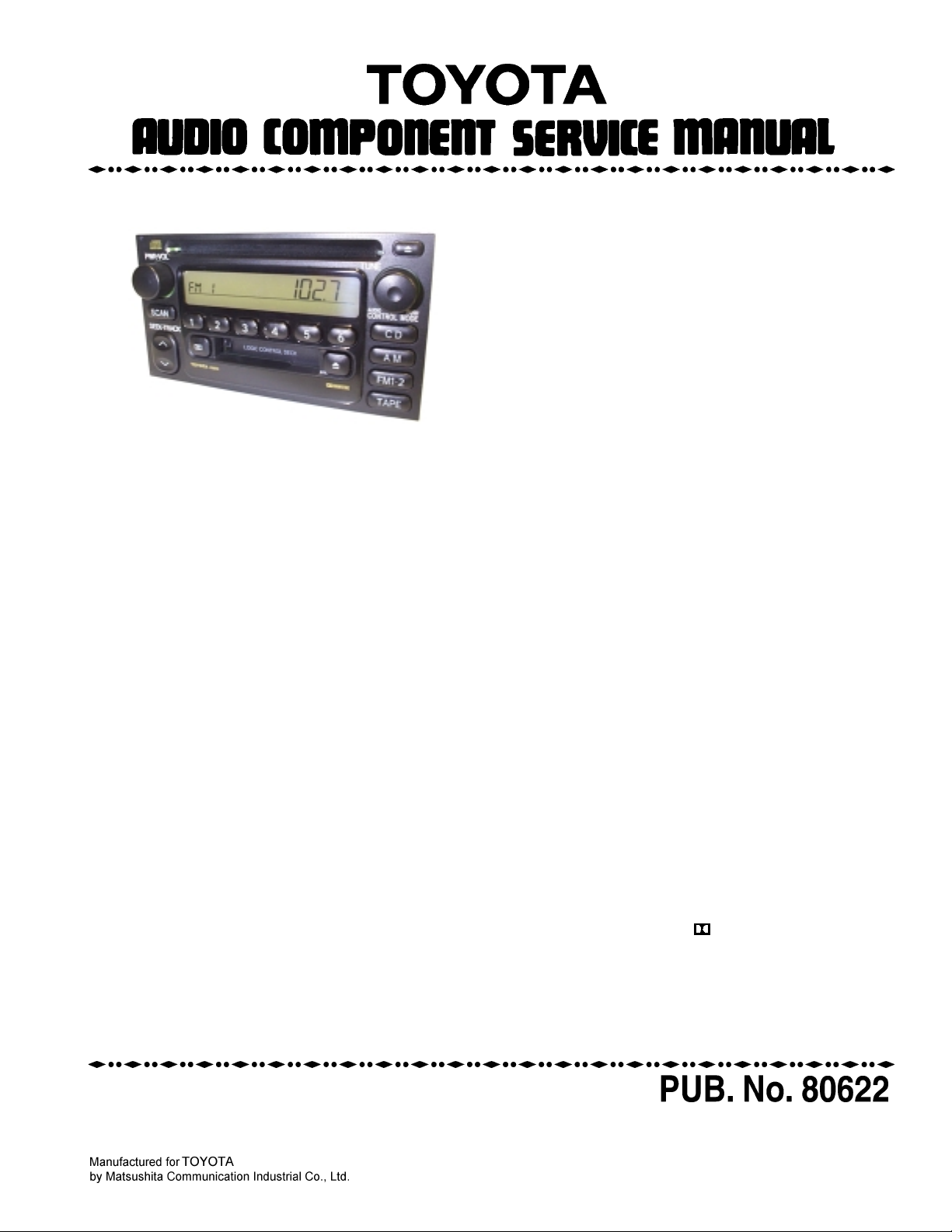
CQ-JT1010X
CQ-JS6910X
AM/FM MPX Radio with Stereo Cassette
Tape Player and CD Player
PART No. (CQ-JT1010X) : 86120-AD020
(CQ-JS6910X) : 86120-2B680
ID CODE (CQ-JT1010X) : A56815
(CQ-JS6910X) : A56814
VEHICLE (CQ-JT1010X) : TACOMA
(CQ-JS6910X) : ECHO, CELICA, MR-S
DESTINATION : North America
PRODUCED AFTER : Mar., 2000
I0
Specifications*
General
Power Supply DC 12V (11V - 16V),
Test Voltage 13.2V
Negative Ground
Current Consumption Less than 2A
Power Output 17W×4
AM Radio
Frequency Range 530 - 1,710 kHz
Usable Sensitivity 25dB/µV (S/N 20dB)
FM Stereo Radio
Frequency Range 87.75 - 107.9MHz
Usable Sensitivity 6dB/µV (S/N 30dB)
CD Player
Signal to Noise Ratio More than 66dB
Total Harmonic Distortion Less than 0.4%
Channel Separation More than 55dB
Cassette Player
Repreduction System 4-Track, 2-Program Stereo
Tape Speed 1-7/8” (4.76cm/sec)
Wow and Flutter Less than 0.3% (WRMS)
Signal to Noise Ratio More than 55dB (IHF-A)
Dimensions**(W×H×D) 178×100×156.5mm
Weight** 2.3kg
* Specifications and the design are subject to possible modification
without notice due to improvements.
** Dimensions and Weight shown are approximate.
Dolby noise reduction manufactured under license from Dolby
Laboratories Licensing Corporation.
“Dolby” and the double-D symbol
Laboratories Licensing Corporation.
are trade marks of Dolby
CQ-JT1010X / CQ-JS6910X
CONTENTS
Page Page
1 FEATUERS 2
2 LASER PRODUCTS
3 FRONT VIEW AND FUNCTIONS
4 REAR VIEW AND CONNECTORS
5 WIRING CONNECTION
6 BLOCK DIAGRAM
7 TERMINALS DESCRIPTION
8 PACKAGE AND IC BLOCK DIAGRAM
9 ALIGNMENT INSTRUCTIONS
10 REPLACEM ENT PARTS LIST
11 EXPLODED VIEW (Unit) 19
2
12 CD PLAYER PARTS
3
13 EXPLODED VIEW (CD Deck)
14 TAPE PLAYER PARTS
3
4
15 EXPLODED VIEW (Tape Deck)
5
16 WIRING DIAGRAM
17 SCHEMAT IC DIAGRAM -1
7
9
18 SCHEMAT IC DIAGRAM -2
12
19 MEMO
13
20
21
22
23
24
34
37
41
1 FEATUERS
·
PLL (Phase Locked Loop) synthesized tuning
·
18-station preset (12-FM, 6-AM)
·
NCD-8 Series CD Deck Mechanism
·
NCA-1 Series Cassette Deck Mechanism
·
Electronic Audio control with Rotary Encoder
·
AVC-LAN Control
2 LASER PRODUCTS
2
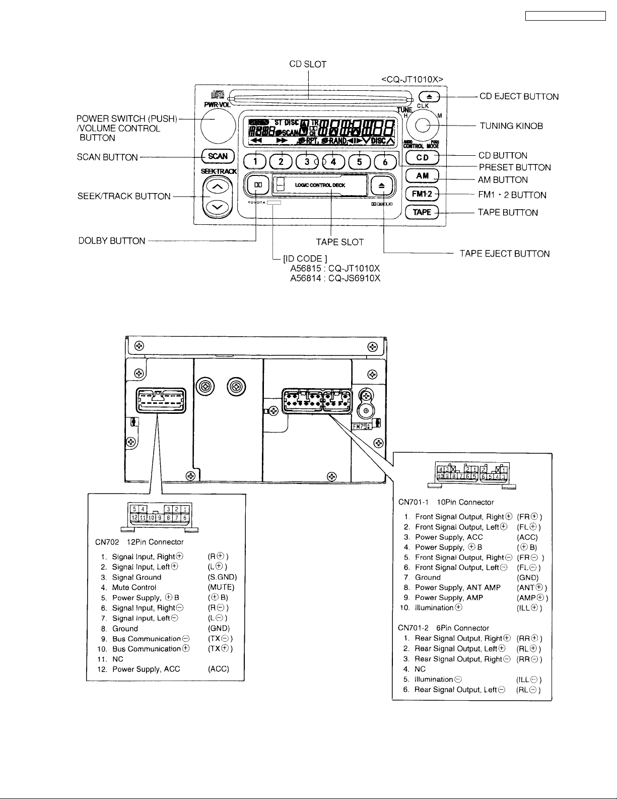
3 FRONT VIEW AND FUNCTIONS
CQ-JT1010X / CQ-JS6910X
4 REAR VIEW AND CONNECTORS
3
CQ-JT1010X / CQ-JS6910X
5 WIRING CONNECTION
4
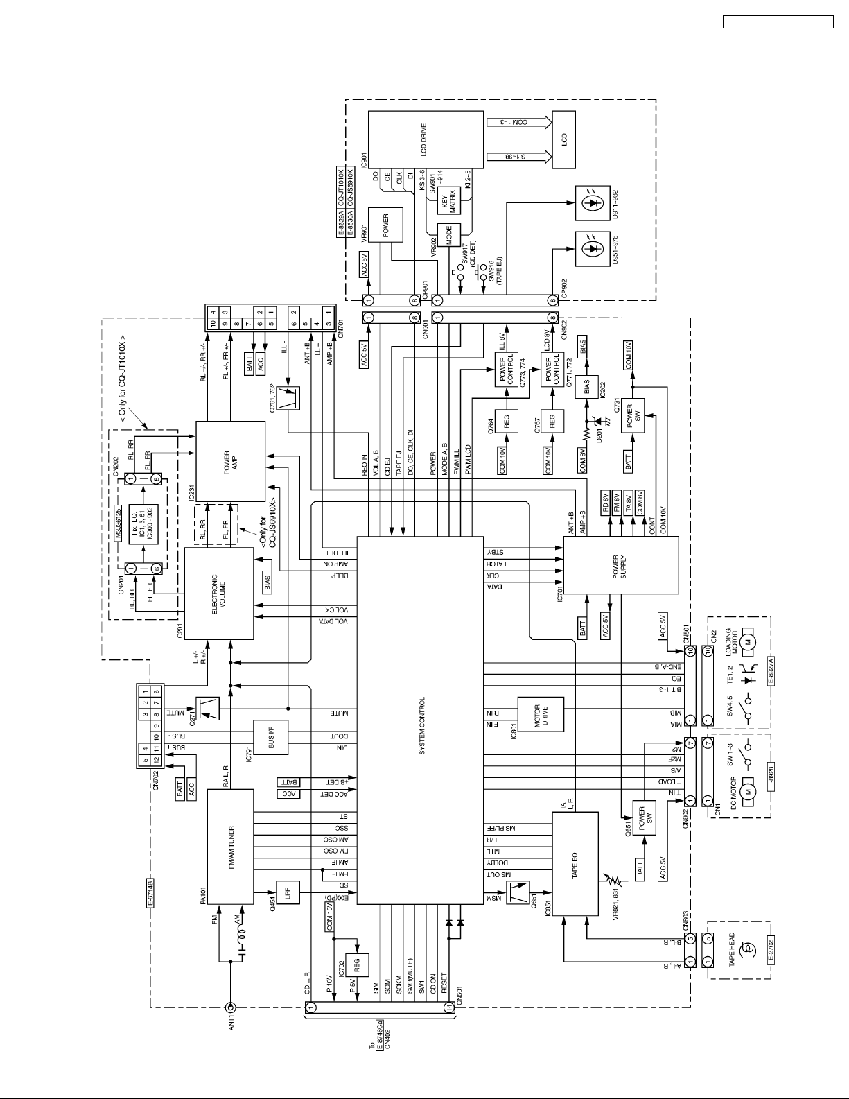
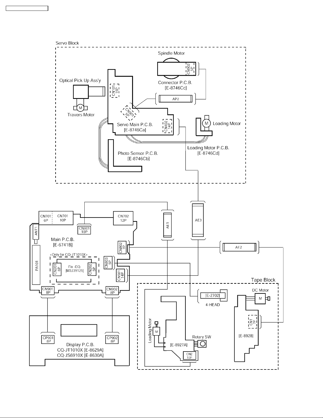
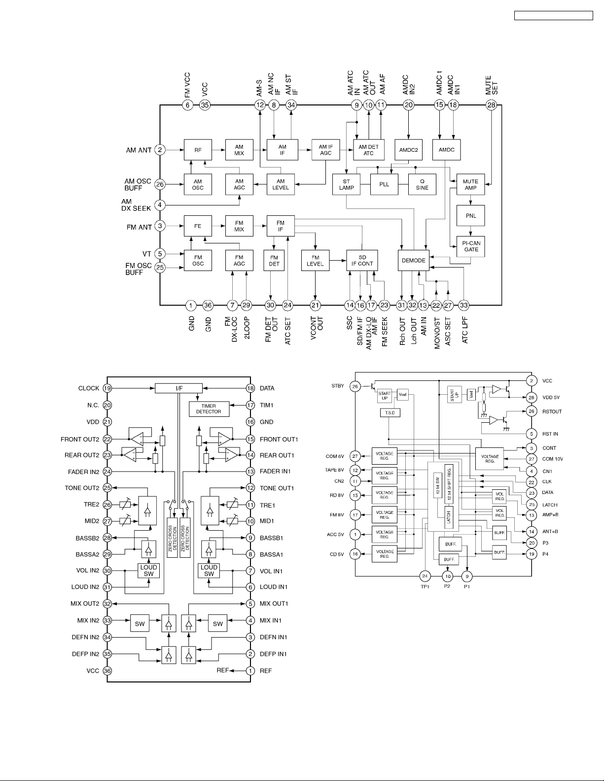
6 BLOCK DIAGRAM
6.1. Main Block
CQ-JT1010X / CQ-JS6910X
5
CQ-JT1010X / CQ-JS6910X
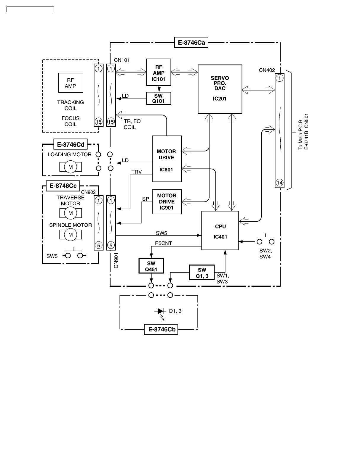
6.2. CD Servo Block
6
7 TERMINALS DESCRIPTION
7.1. Main Block
IC601 : C2BBGF000090
Pin
Port Descriptions I/O FM
No.
1 STBY Power Control IC
2 LATCH Power Control IC Latch
3 CD SOM CD Serial Data Input I 0 0 1.5 0
4 CD SIM CD Serial Data Output O 0 0 0 0
5 CD SCKM CD Serial Data Clock O 0 0 4.9 0
6 MUTE H: Mute ON, L: Mute OFF O 0 0 0 0
7 DATA Power Control IC Data O 0 0 0 0
8 CLK Power Control IC Cloock O 0 0 0 0
9 EQ Metal tape Detection I 4.8 4.8 4.8 0
10 BIT3 Tape Rotary Switch 3 I 4.8 4.8 4.8 0
11 BIT2 Tape Rotary Switch 2 I 4.8 4.8 4.8 4.8
12 BIT1 Tape Rotary Switch 1 I 0 0 0 4.8
13 VOL CK Electronic Volume Clock O 0 0 0 0
14 VOL DATA Electronic Volume Data O 0 0 0 0
15 RIN Tape Control O 0 0 0 0
16 FIN Tape Control O 0 0 0 0
17 RADIIO
MUTE
18 IFZ IF Noise Control I 4.8 4.8 4.8 4.8
19 DX/LOC - - 0 0 0 0
20 ST H: Stereo, L: Monoral i 0 1.8 0 0
21 SSC Search Stop Clear O 0 0 0 0
22 SD Radio Signal Detect I 0 0 0 0
23 REO IN Reostat Signal Input I 0 0 0 0
24 ACC DET ACC Votage Detect I 1.9 1.9 1.9 1.9
25 +B DET BATT Voltage Detect I 0 1.8 1.8 1.8
26 ILL DET Illumi. Detection I 2.3 2.3 2.4 2.3
27 VDD +5V Power supply - 4.9 4.9 4.9 4.9
28 VSM (Connecting to Ground) - 0 0 0 0
29 MAIN VOL (Connecting to Ground) - 0 0 0 0
30 GND (Connecting to Ground) - 0 0 0 0
31 GND (Connecting to Ground) - 0 0 0 0
32 GND Ground - 0 0 0 0
33 REG CPU CPU Regulator Terminal - 3.4 3.4 3.4 3.4
34 VDD0 +5V Power Supply - 4.9 4.9 4.9 4.9
35 REG OSC Oscillate Terminal - 4.9 4.9 4.9 4.9
36 X2 Main System X-tal I 1.9 1.9 1.9 1.9
37 X1 Main System X-tal O 2.1 2.1 2.1 2.1
38 GND 0 Ground - 0 0 0 0
39 NC - - - - - 40 GND 2 Ground - 0 0 0 0
41 AM IF AM IF Counter I 0 2.0 0 0
42 FM IF FM IF Counter I 2.0 0 0 0
43 VDD PLL +5V Power supply - 4.8 4.8 4.8 4.8
44 FM OSC FM Oscillator Input I 2.5 0 0 0
45 AM OSC AM Oscillator Input I 0 1.8 0 0
46 GND PLL Ground (for PLL) - 0 0 0 0
47 EO 0 Phase Detecter Output O 1.4 1.4 0 1.4
48 (NC) - - - - - 49 IC (VPP) IC VPP Terminal I 0 0 0 0
50 RESET Reset Control Input I 4.8 4.8 4.8 4.8
51 VOL B Rotary Encoder I 4.8 4.8 0 4.8
52 VOL A Rotary Encoder I 0 0 0 4.8
53 RESMONI 4.5V Detect Monitor O 4.9 4.9 4.9 4.9
54 LCD DO LCD Driver Data Input I 4.8 4.8 4.9 4.8
55 LCD DI LCD Driver Data Output O 0 0 0 0
56 LCD CE LCD Driver Chip Enable O 0 0 0 0
57 LCD CLK LCD Driver Clock O 0 0 0 0
58 POWER POWER Switch Signal I 4.8 4.8 4.8 4.8
59 BEEP Beep Sound Output O 0 0 0 0
60 (NC) - - 0 0 0 0
61 PWM ILL Illumi. Power Control O 7.6 7.6 7.6 7.6
62 PWM LCD LCD Power Control O 7.6 7.6 7.6 7.6
63 M2F Tape Motor Control O 0 0 0 0.5
64 (NC) - - - - - -
Standby Control
Control
- - 0 0 0 0
(V)AM(V)CD(V)TP(V)
O 4.9 4.8 4.9 4.8
O 4.9 4.9 4.9 4.9
CQ-JT1010X / CQ-JS6910X
Pin
Port Descriptions I/O FM
No.
65 (NC) - - - - - 66 (NC) - - - - - 67 DIV MAIN - - 0 0 0 0
68 DIV SUB - - 0 0 0 0
69 SO (NC) - - 0 0 0 0
70 SI (NC) - - 0 0 0 0
71 LCD ON - - 0 0 0 0
72 ILL ON - - 0 0 0 0
73 DIN AVC LAN Data Output O 0 0 0 0
74 D OUT AVC LAN data Input I 0 0 0 0
75 (NC) - - 0 0 0 0
76 MODE B Rotary Encoder(MODE SW) I 0 0 0 0
77 MODE A Rotary Encode (MODE SW) I 0 0 0 0
78 TAPE EJ TAPE EJECT Key I 4.8 4.8 4.8 4.8
79 CD EJ CD EJECT Key I 4.8 4.8 4.8 4.8
80 INTERS 4.5V Detect Interrupt I 4.9 4.9 4.9 4.9
81 SETUP 2 - - - - - 82 GND1 Ground - 0 0 0 0
83 SW1 Disc Detect Switch 1 I 0 0 3.9 0
84 SW3 Disc Detect Switch 3 I 0 0 4.2 0
85 CD ON CD CPU Stundby O 0 0 4.9 0
86 CD RESET CD CPU Reset O 4.9 4.9 4.9 4.9
87 MS PL/FF Tape Mode Control O 0 0 0 0
88 F/R Tape A/B Side Signal O 0 0 0 0
89 MTL Tape Metal Control O 0 0 0 4.8
90 DOLBY Tape Dolby Control O 0 0 0 4.9
91 MS OUT Tape Music Sensor
92 MSM Tape blank Signal
93 AMP ON AMP Power Control O 4.8 4.8 4.8 4.8
94 TIN Tape In Detect I 4.8 4.8 4.8 0
95 T LOAD Tape Position Detect I 4.8 4.8 4.8 0
96 A/B Tape A/B Side Signal I 0 0 0 0
97 END A Tape End Detect A I 0 0 0 0
98 END B Tape End Detect B I 4.7 4.7 4.7 0
99 VDD +5V Power supply - 4.9 4.9 4.9 4.9
100 GND Ground - 0 0 0 0
Detection
Detect Sensitivity
(V)AM(V)CD(V)TP(V)
I 4.8 4.8 4.8 0
O 0 0 0 4.8
Note 1 : Voltage measuerments are with respect to ground,
with a voltmeter (internal resistance : 10M ohms).
7.2. Display Block
IC901 : C0HBA0000016
Pin
No.
1-38 SEG1-38 LCD segment data O 2.4
39,40 SEG39,40 Not used - 41-43 COM1-3 LCD common O 2.4
44 KS1/S41 Not used - 45 KS2/S42 Not used - -
46-49 KS2-9 Key scan O 4.8
50 KI1 Not used - -
51-54 KI2-5 Key data I 0
55 TEST (Connecting to ground) - 0
56 VDD +5V power supply - 4.8
57 VDD1 Ground through capacitor terminal - 3.2
58 VDD2 Ground through capacitor terminal - 1.6
56 Vss Ground - 0
60 OSC CR oscillator terminal - 3.8
61 DO LCD data O 4.8
62 CE LCD driver chip enable I 0
63 CL Clock for LCD I 0
64 DI LCD data I 0
Port Descriptions I/O Vol.
(V)
7
CQ-JT1010X / CQ-JS6910X
7.3. CD Servo Block
IC201 : MN662748RPMF
Pin
No.
1 BCLK Not used - 2 LRCK Not used - 3 SRDATA Not used - 4 DVDD +5V digital power supply - 5.0
5 DVSS1 Digital ground - 0
6 TX Not used - 7 MCLK MPU command clock I 0
8 MDATA MPU command data I 0
9 MLD MPU command load I 0
10 SENSE Sense signal O 0
11 /FLOCK Focus servo lock O 0
12 /TLOCK Tracking servo lock O 4.9
13 BLKCK Not used - 14 SQCK Q code external clock I 4.9
15 SUBQ Q code output O 2.5
16 DMUTE DSP mute I 0
17 STAT DSP Status output O 3.1
18 /RST Reset input I 4.9
19,20 Not used - -
21 TRV Forced traverse output O 2.5
22 TVD Traverse drive output O 2.5
23 PC Spindle motor control O 0
24 ECM Spindle motor drive O 2.5
25 ECS Spindle motor drive O 2.5
26 KICK Kick pulse output O 2.5
27 TRD Tracking motor drive O 2.5
28 FOD Focus motor drive O 2.5
29 VREF D/A reference voltage I 2.5
30 FBAL Focus balance adjust O 2.5
31 TBAL Tracking balance adjust O 2.5
32 FE Focus error signal I 2.5
33 TE Tracking error signal I 2.5
34 RFENV RF envelope signal I 2.5
35 VDET Vibration detection I 0
36 OFTR Off track signal I 0
37 TRCRS Track closs signal I 2.1
38 /RFDET RF detection signal I 0
39 BDO Drop out signal I 0
40 LDON Laser on/off control O 4.5
41 PLLF2 Not used - 42 TOFS TE offset O 2.5
43 WVEL Not used - 44 ARE RF signal I 1.7
45 IREF Reference current input I 1.6
46 DRF DSL bias I 0
47 DSLF DSL loop filter I/O 2.4
48 PLLF PLL loop filter I/O 1.8
49 VCOF Not used - 50 AVDD2 +5V analog power supply - 5.0
51 AFSS2 Analog ground - 0
52 EFM Not used - 53 PCK/DSLB DSL bias I 2.4
54 VCOF2 Tracking offset O 2.5
55 SUBC Not used - 56 SBCK (Connecting to ground) - 57 VSS Ground - 0
58 X1 Crystal oscillator I 1.7
59 X2 Crystal oscillator O 2.3
60 VDD +5V power supply - 5.0
61,62 - Not used - -
63 FCLK Not used - -
Port Description I/O (V)
64 IPFLAG Not used - 65 FLAG Not used - -
66-69 - Not used - -
70 IOSEL (Connecting to ground) I 0
71 /TEST (Connecting to ground) I 0
72 AVDD1 +5V analog power supply - 4.9
73 OUTL Audio Lch output O 4.9
74 AVSS1 Analog ground - 0
75 OUTR Audio Rch output O 4.9
76 RSEL (Connecting to ground) - 0
77 CSEL (Connecting to ground) - 0
78 PSEL (Connecting to ground) - 0
79 MSEL (Connecting to ground) - 0
80 SSEL mode select I 5.0
IC401 : MN101C117AG
Pin
No.
1 MASHON Servo IC OSC control O 5.0
2 P82 No connection - 3 P81 No connection - 4 P80 (Connection to ground) - 0
5 Q1 Photo sensor signal (DISC IN) I 4.5
6 Q3 Photo sensor signal (DISC OUT) I 4.2
7 Q6 Photo sensor signal (Option) I 5.0
8 SW4 Clamp SW signal I 0
9 SW5 Inner SW signal I 5.0
10 SW2 Feeder arm SW I 5.0
11 PA6 (Connection to ground) - 0
12 PA7/IFR (Connecting to ground) I 0
13 VDD +5V power supply - 5.0
14 OSC2 Crystal oscillator - 5.0
15 OSC1 Crystal oscillator - 3.3
16 VSS Ground - 0
17 NC No connection - 18 SOMI CD control data O 3.2
19 SIMO CD control data I 3.8
20 SCLM Data shift clock I 5.0
21 P06 Not used - 22 BD0 Drop out signal I 0
23 PC1 Loading motor driver control O 5.0
24 PS2 Focus/Tracking driver control O 0
25 VDET Vibration detecting signal I 0
26 P14 No connection - 27 CDON CD on signal I 5.0
28 IRQ1.SENSE(Connecting to groung) - 0
29 IRQ2 (Connecting to ground) - 0
30 LOD Loading motor control - 2.6
31 TRV Traverse motor control - 2.5
32 /PRST Servo IC reset O 5.0
33 STAT Status signal I 4.0
34 DMUTE DSP mute O 0
35 SUBQ Sub code Q data I 2.6
36 SQCK Sub code Q clock O 5.0
37 /TLOCK Tracking servo lock I 0
38 /FLOCK Focus servo lock I 0
39 NRST reset input I 5.0
40 MMOD (Connecting to ground) - 0
41 SENSE Sense signal I 0
42 MLD Command load O 5.0
43 MDATA Command data O 0.9
44 MCLK Command clock O 4.6
Port Description I/O (V)
8
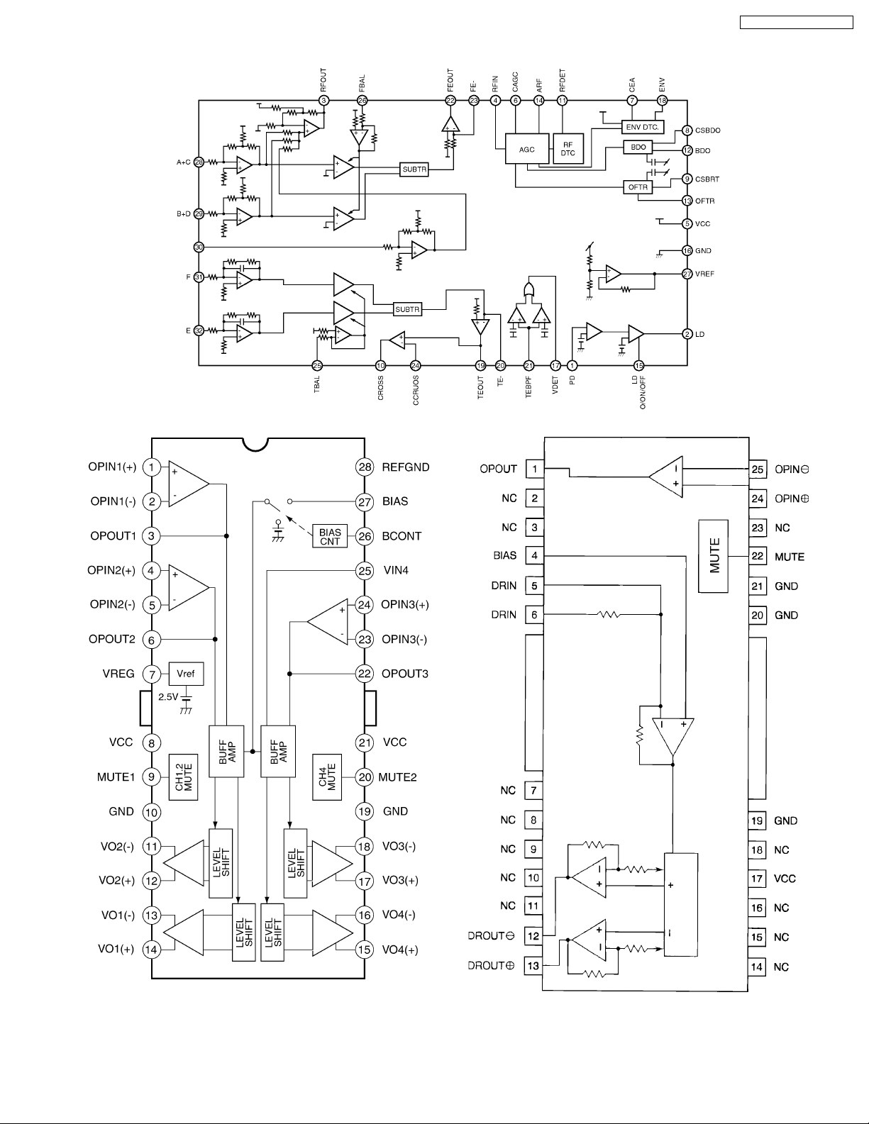
8 PACKAGE AND IC BLOCK DIAGRAM
8.1. Main Block
CQ-JT1010X / CQ-JS6910X
PA101 : YMP0PTA514B0
IC701 : C0DBZHZ00005
IC201 : C1BB00000284
9
CQ-JT1010X / CQ-JS6910X
IC231 : AN7550NZ
IC202 : YEAMPC4570E1
IC801 : C0GBG0000004
IC791 : C1BB00000034
10
8.2. CD Servo Block
CQ-JT1010X / CQ-JS6910X
IC101 : C1BB00000173
IC601 : C0GBY0000004
IC901 : C0GBY0000003
11
CQ-JT1010X / CQ-JS6910X
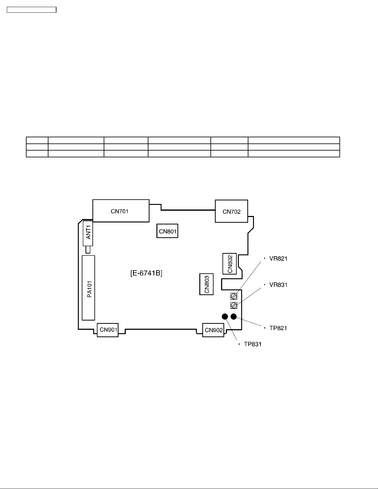
9 ALIGNMENT INSTRUCTIONS
9.1. Alignment Conditions
·
Power Supply Voltage : DC13.2V
·
Output Impedance : 4
·
Output Power : 0.5W
Notes:
Do not align the FM/AM package blocks. When the package block is necessary, it will be supplied already aligned at
the factory.
Ω
·
Balance, Fader Control : center
·
Bass, Treble Control : Center
9.2. Dolby NR Alignment
Step Alignment Item Test Tape VTVM Connection Adjust Remarks
(1) DOLBY NR Rch RFKZ0038 TP821 VR821 Adjust for 388mV ±0.5dB
(2) DOLBY NR Lch RFKZ0038 TP831 VR831 Adjust for 388mV ±0.5dB
9.3. Alignment Points
12
10 REPLACEMENT PARTS
LIST
Notes :
1. Be sure to make your orders of replacement parts
according to this list.
2. Important safety notice: Components, identified by
have special characteristics important for safety. When
replacing any of these components, use only
manufacturer´s specified parts.
3. Location keys in the remarks column indicates the general
location of the parts shown in the exploded drawing, as in a
road map.
4. The marking (RTL) indicates that Retention Time is limited
for this item. After the discontinuation of assembly in
production, the item will continue to be available for a
specific period of time. The retention period of availability is
dependent on the type of assembly, and in accordance with
the laws governing part and product retention. After the end
of this period, the assembly will no longer be available.
5. "MCC" marks in remarks column are indicated supply parts
of Matsushita Communication Industrial Corp. of America
(MCC).
6. "A" or "B" marks in remarks column are indicated as
follows :
·
A : CQ-JT1010X
·
B : CQ-JS6910X
Ref.
No.
[E6741B] Main Block
IC´s and TRANSISTORs
IC201 C1BB00000284 IC
IC202 YEAMPC4570E1 IC
IC231 AN7550NZ IC
IC601 C2BBGF000090 IC
IC701 C0DBZHZ00005 IC
IC702 AN7805 IC
IC791 C1BB00000034 IC
IC801 C0GBG0000004 IC
IC851 C1BB00000100 IC
PA101 YMP0PTA514B0 Electronic Tuner MCC
Q271 B1GDCFNN0003 Transistor
Q451 B1CBGF000001 Transistor
Q651 2SB14460HA Transistor
Q731 B1BCDG000005 Transistor
Q761 B1GDCFNN0003 Transistor
Q762 B1GBCFNN0005 Transistor
Q764 B1BBCF000009 Transistor
Q767 B1BBCF000009 Transistor
Q771 2SD10300HL Transistor
Q772 2SB14400HL Transistor
Q773 2SD10300HL Transistor
Q774 2SB14400HL Transistor
Q851 B1GBCFJN0005 Transistor
DIODEs
D201 B0BC3R900008 Diode
D271 B0ACCE000001 Diode
D272 MA151WKTX Diode
D273 B0ACCE000001 Diode
D686 MA151WATX Diode
D700 B0JCPE000004 Diode
D701 B0EANM000003 Diode
D751 B0BC4R600003 Diode
D752 B0BC4R600003 Diode
Part No. Part Name & Description Remarks
mark
Ref.
No.
D753 B0BC4R600003 Diode
D754 B0ECKL000001 Diode
D755 B0ECKL000001 Diode
D761 B0BC5R000004 Diode
D771 B0BC8R100002 Diode
D772 B0BC8R100002 Diode
D791 B0BC5R600004 Diode
D792 B0BC5R600004 Diode
D821 B0ACCE000001 Diode
D831 B0ACCE000001 Diode
D871 MA151WATX Diode
R235 B0BC01000003 Diode
CAPACITORs
C50 F1J1H120A025 Ceramic, 12PF 50WV
C51 F1J1H102A509 Ceramic, 1000PF 50WV
C56 F1J1H102A509 Ceramic, 1000PF 50WV
C57 F1J1H102A509 Ceramic, 1000PF 50WV
C100 ECA1CM100I Electrolytic, 10µF 16WV
C101 F1J1H103A509 Ceramic, 0.01µF 50WV
C105 YECUS1C224KX Ceramic, 0.22µF 16WV
C106 F1J1H103A509 Ceramic, 0.01µF 50WV
C107 F1J1E223A002 Ceramic, 0.022µF 25WV
C108 EEUFC1A221B Electrolytic, 220µF 10WV
C109 F1J1E223A002 Ceramic, 0.022µF 25WV
C121 F1J1E223A002 Ceramic, 0.022µF 25WV
C122 F1J1H103A509 Ceramic, 0.01µF 50WV
C123 ECA1HM2R2I Electrolytic, 2.2µF 50WV
C131 F1J1E223A002 Ceramic, 0.022µF 25WV
C132 F1J1H103A509 Ceramic, 0.01µF 50WV
C133 ECA1HM2R2I Electrolytic, 2.2µF 50WV
C151 F1J1H151A034 Ceramic, 150PF 50WV
C152 F1J1H471A025 Ceramic, 470PF 50WV
C153 ECA1CM100B Electrolytic, 10µF 16WV
C155 F1J1H103A509 Ceramic, 0.01µF 50WV
C156 F1J1E223A002 Ceramic, 0.022µF 25WV
C157 EEUFC1A221B Electrolytic, 220µF 10WV
C201 F1J1H103A509 Ceramic, 0.01µF 50WV
C202 ECA0JM331B Electrolytic, 330µF 6.3WV
C203 ECA1HM010B Electrolytic, 1µF 50WV
C204 ECA1HM010B Electrolytic, 1µF 50WV
C205 YECUS1A105KX Ceramic, 1µF 10WV
C206 F1J1H102A509 Ceramic, 1000PF 50WV
C208 F1J1C6830001 Ceramic, 0.068µF 16WV
C209 F1J1C6830001 Ceramic, 0.068µF 16WV
C210 F1J1H103A509 Ceramic, 0.01µF 50WV
C211 YECUS1A105KX Ceramic, 1µF 10WV
C214 F1J1E4730003 Ceramic, 0.047µF 25WV
C216 F1J1E333A002 Ceramic, 0.033µF 25WV
C217 ECA1HMR33B Electrolytic, 0.33µF 50WV
C218 F1J1E4730003 Ceramic, 0.047µF 25WV
C231 YECUV1C224KX Ceramic, 0.22µF 16WV
C232 YECUV1C224KX Ceramic, 0.22µF 16WV
C233 YECUV1C224KX Ceramic, 0.22µF 16WV
C234 YECUV1C224KX Ceramic, 0.22µF 16WV
C235 ECA1CM330B Electrolytic, 33µF 16WV
C271 ECA1HM010B Electrolytic, 1µF 50WV
C281 F1J1H221A025 Ceramic, 220PF 50WV
C282 F1J1H221A025 Ceramic, 220PF 50WV
C301 F1J1H103A509 Ceramic, 0.01µF 50WV
C302 ECA1CM470B Electrolytic, 47µF 16WV
C303 ECA1HM010B Electrolytic, 1µF 50WV
C304 ECA1HM010B Electrolytic, 1µF 50WV
C305 YECUS1A105KX Ceramic, 1µF 10WV
C306 F1J1H102A509 Ceramic, 1000PF 50WV
C308 F1J1C6830001 Ceramic, 0.068µF 16WV
C309 F1J1C6830001 Ceramic, 0.068µF 16WV
C310 F1J1H103A509 Ceramic, 0.01µF 50WV
C311 YECUS1A105KX Ceramic, 1µF 10WV
C314 F1J1H103A509 Ceramic, 0.01µF 50WV
C315 ECA1CM470B Electrolytic, 47µF 16WV
C316 F1J1E333A002 Ceramic, 0.033µF 25WV
Part No. Part Name & Description Remarks
CQ-JT1010X / CQ-JS6910X
13
 Loading...