

Panasonic CQJA-1920-L, CQJA-1924-L Service manual
ORDER No. AED0101023
AUTOMOTIVE ELECTRONICS
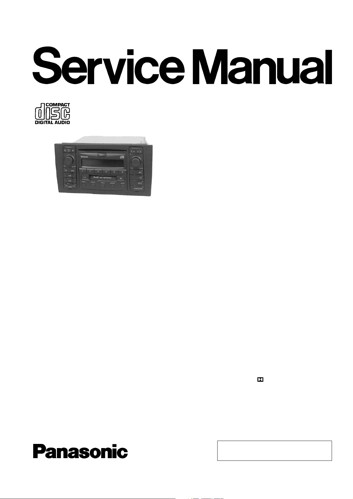
AUDI
CQ-JA1920L
CQ-JA1924L
AM/FM MPX ELECTRONIC TUNING
RADIO with Stereo Cassette Tape
Player and CD Player
AUDI No. (CQ-JA1920L) : 8D0 035 195E
AUDI No. (CQ-JA1924L) : 8Z0 035 196
VEHICLE (CQ-JA1920L) : Audi A4
VEHICLE (CQ-JA1924L) : Audi A2
Specification
General
Power Supply DC 12V (11V - 16V),
Test Voltage 13.2V
Negative Ground
Current Consumption Less than 4.0A
Power Output 12W×12W
Speaker Impedance 4Ω
AM Radio
Frequency Range 531 - 1,6020kHz
Signal to Noise Ratio 23dB(µV) (S/N 20dB)
FM Stereo Radio
Frequency Range 87.5 - 108.0MHz
Usable Sensitivity 5dB/µV (S/N 30dB)
CD Player
Signal to Noise Ratio More than 90dB
Channel Separation More than 80dB
DESTINATION : Europe
SALE DATE : May., 2000
Total Harmonic Distortion Less than 0.02%
Tape Player
Reproduction System 4-Track, 2-Program Stereo
Tape Speed 1-7/8” (4.76cm/se c)
Signal to Noise Ratio More than 42dB
Wow and Flutter 0.09% (WRMS)
Stereo Separation More than 30dB
Dimensions** 178×164.5×110mm
* Specifications and the design are subject to possible modification
without notice due to improvements.
** Dimensions and Weight shown are approximate.
Doldy noise reduction manufactured under license from Dolby
Laboratories Licensing Corporation.
“Dolby” and the double-D symbol
Laboratories Licensing Corporation.
are trade marks of Dolby
© 2001 Matsushita Communication Industrial Co.,
Ltd. All rights reserved. Unauthorized copying and
distribution is a violation of law.

This file was downloaded and provided FREE OF CHARGE
from the ManualDirectory community.
You can find many free to download Service Manuals & Schematics at
http://www.manualdirectory.co.uk
AUDI / CQ-JA1920L / CQ-JA1924L
CONTENTS
Page Page
1 FEATUERS 2
2 LASER PRODUCTS
3 REAR VIEW AND CONNECTORS
4 FRONT VIEW AND FUNCTIONS
5 ALIGNMENT INSTRUCTIONS
6 ALIGNMENT POINTS
7 WIRING CONNECTION
8 BLOCK DIAGRAM
9 TERMINALS DESCRIPTION
10 PACKAGE AND IC BLOCK DIAGRAM
11 REPLACEMENT PARTS LIST 16
2
12 EXPLODED VIEW (Unit)
2
13 CD PLAYER PARTS
14 EXPLODED VIEW (CD Deck)
3
4
15 TAPE PLAYER PARTS
4
16 EXPLODED VIEW (Tape Deck)
17 WIRING DIAGRAM
5
6
18 SCHEMAT IC DIAGRAM -1
8
19 SCHEMAT IC DIAGRAM -2
12
25
26
28
29
30
31
40
41
1 FEATUERS
±
PLL (Phase Locked Loop) synthesized tuning.
±
24-station preset (12-AM, 12-FM).
±
RDS function.
±
Diversity function.
±
Dolby Noise Reduction System.
±
CD changer control.
±
BOSE specification correspondence.
±
Anti-theft system.
±
CAN-BUS I/F.
2 LASER PRODUCTS
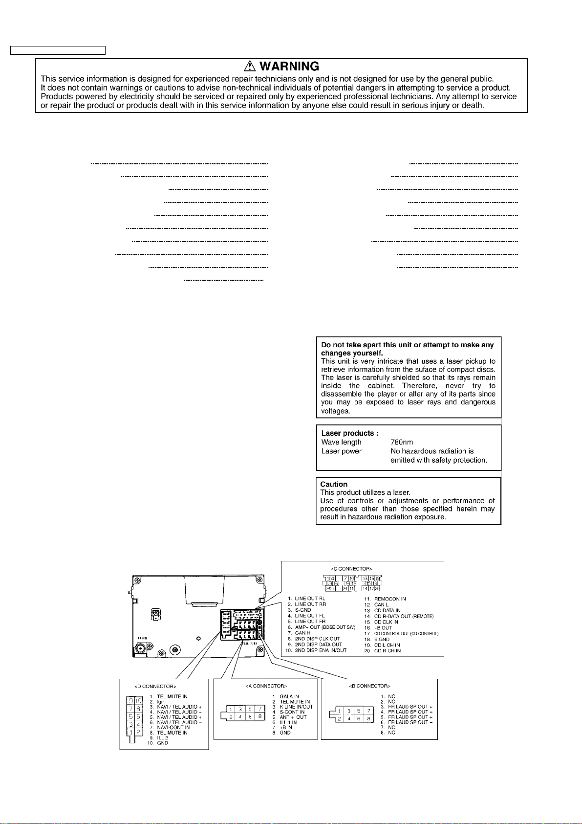
3 REAR VIEW AND CONNECTORS
2
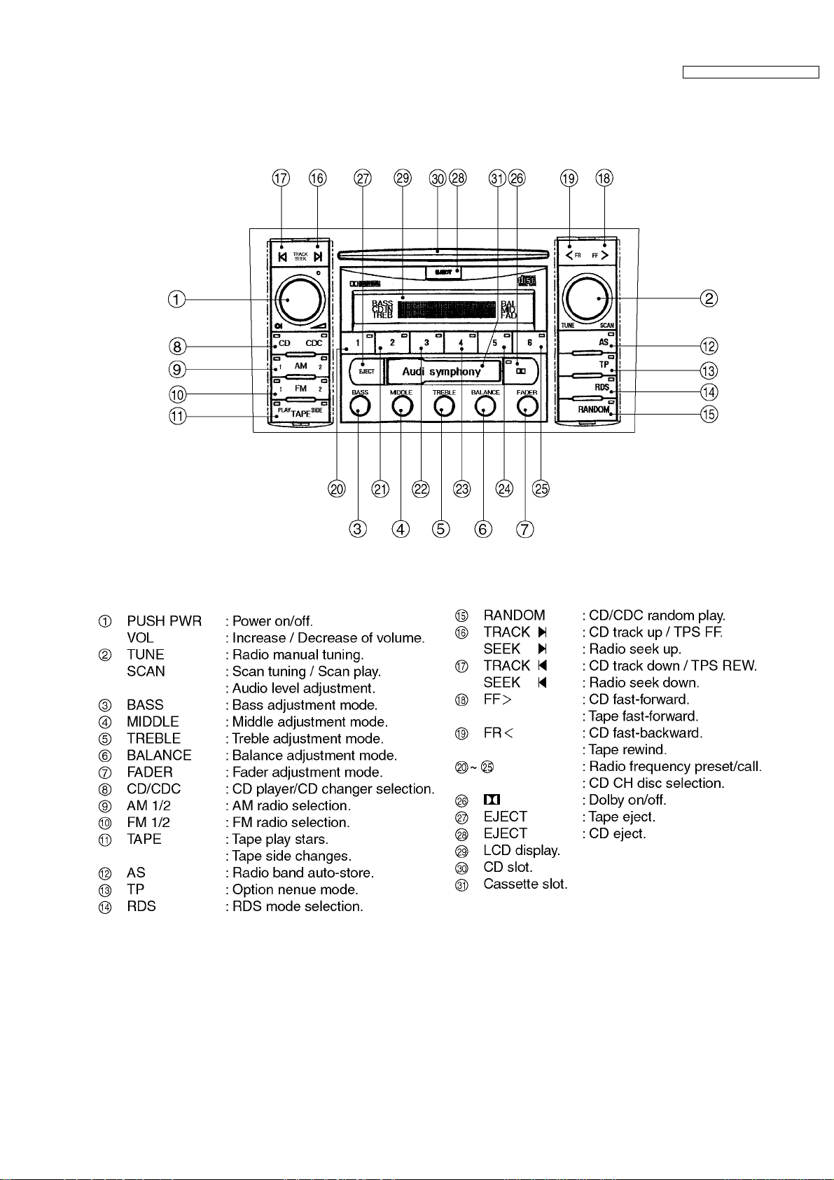
4 FRONT VIEW AND FUNCTIONS
AUDI / CQ-JA1920L / CQ-JA1924L
3
AUDI / CQ-JA1920L / CQ-JA1924L
5 ALIGNMENT INSTRUCTIONS
5.1. Alignment Conditions
±
Power Supply Voltage : DC13.2V
±
Output Impedance : 4
±
Output Power : 0.5W
Note :
Do not align the FM/AM package block. When the package block is necessary, it will be supplied already aligned at the
factory.
Ω
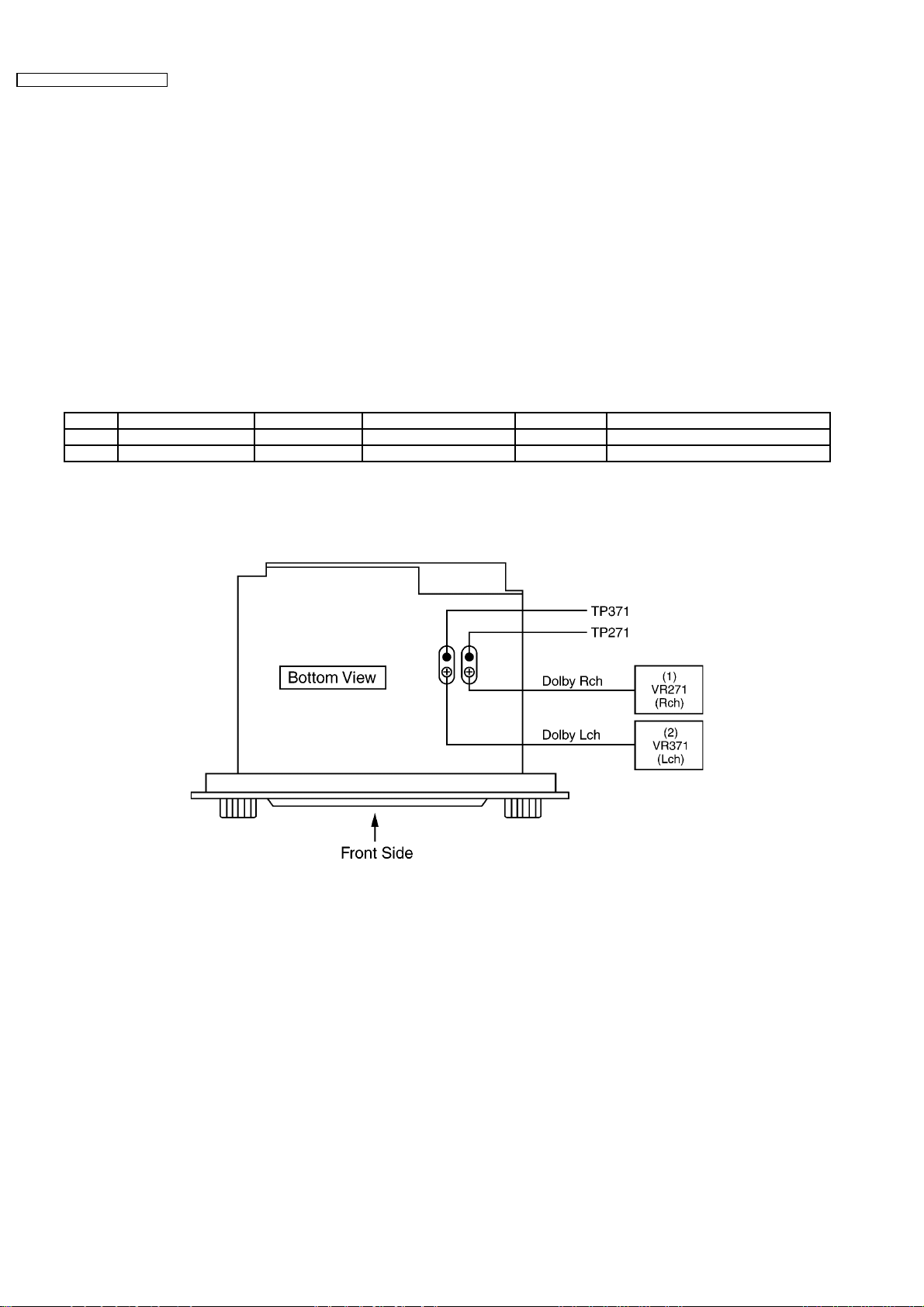
5.2. Dolby NR Alignment
Step Alignment Item Test Tape VTVM Connection Adjust Remarks
(1) DOLBY NR Rch RFKZ0038 TP271 VR271 Adjust for 388mV ±0.5dB
(2) DOLBY NR Lch RFKZ0038 TP371 VR371 Adjust for 388mV ±0.5dB
6 ALIGNMENT POINTS
±
Balance, Fader Control : center
±
Bass, Treble Control : Center
±
Dolby NR: OFF
4
7 WIRING CONNECTION
AUDI / CQ-JA1920L / CQ-JA1924L
5
AUDI / CQ-JA1920L / CQ-JA1924L
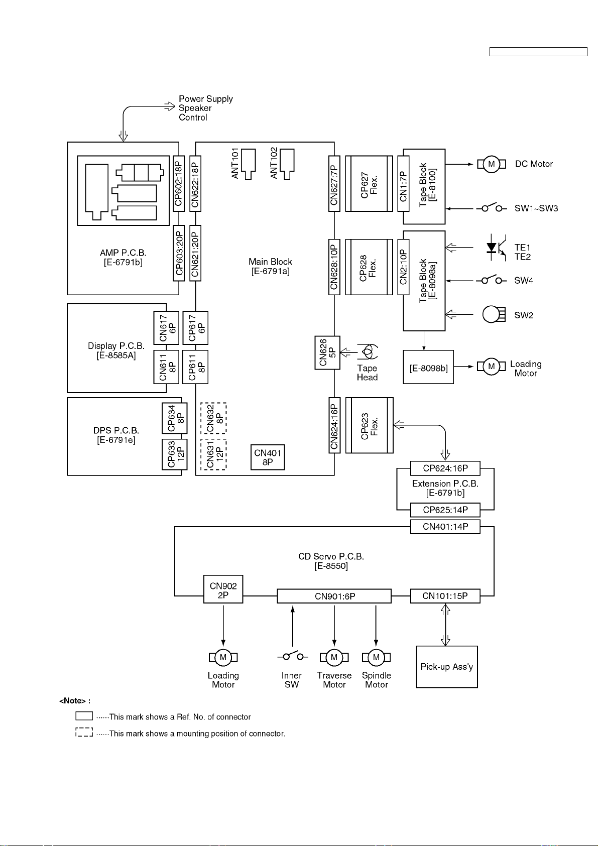
8 BLOCK DIAGRAM
8.1. Main Block
6
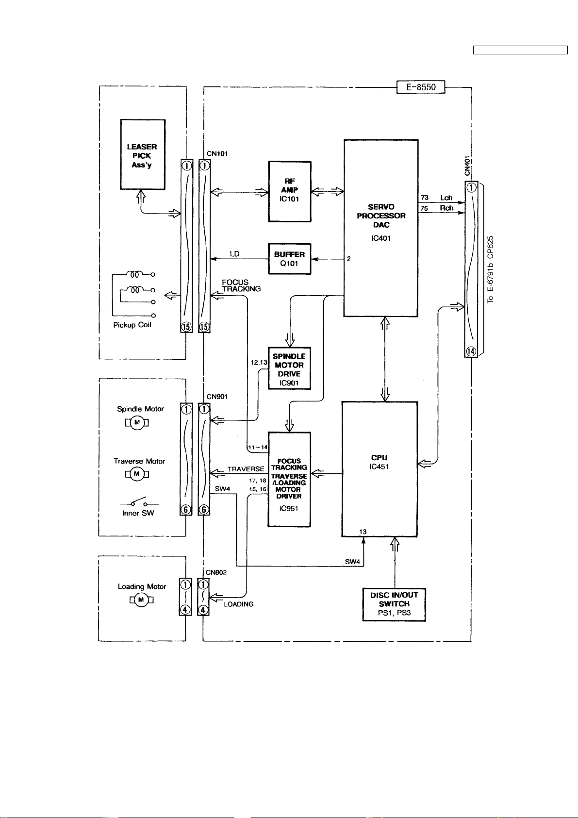
8.2. CD Servo Block
AUDI / CQ-JA1920L / CQ-JA1924L
7
AUDI / CQ-JA1920L / CQ-JA1924L
9 TERMINALS DESCRIPTION
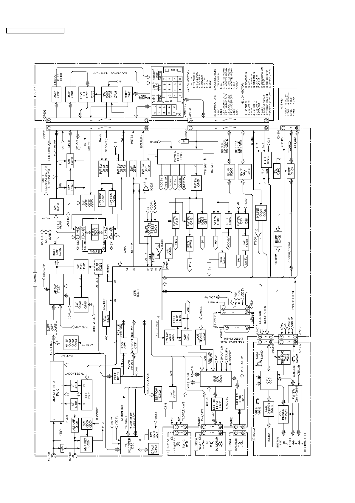
9.1. Main Block
IC621 : C2CBKJ000009
Pin
No.
1 MD1 (Connecting to VDD) - 5.2
2 MD2 MPU mode setting I 4.4
3 NC No connector - 4 NC No connector - 5 CD RESET CD reset O 5.1
6 CD ON CD controller enable O 5.1
7 TIM-SP TIM O 0
8 TIM-ST TIM strobe O 0
9 VSS Ground - 0
10 TIM-REC/PLAY TIM recode/play O 0
11 VCC +3V power supply - 3.0
12 PLL CE PLL chip enable O 0
13 PLL CLK PLL clock O 0
14 PLL DI PLL data O 0
15 VSS Ground - 0
16 PLL DO PLL data I 4.9
17 PVCC1 +5V power supply - 5.2
18 NC No connector - 19 DSP-SI DSP serial data O 0
20 DSP-CLK DSP Clock for serial data O 5.2
21 DSP-RST DSP reset O 0
22 DSP-WRQ DSP data write request O 0
23 DSP-WRDY DSP write ready I 0
24 DSP-CS DSC chip select O 5.1
25 6.5V-DET 6.5V detection I 5.2
26 FLASH-TXD2 Not used - 27 FLASH-RXD2 Not used - 28 AF-MUTE Audio mute control O 5.1
29 VSS Ground - 0
30 MUTE1 Mute control O 5.1
31 MUTE2 Mute control O 5.1
32 F.IN Tape loading motor control O 0
33 R.IN Tape loading motor control O 0
34 CAN-IRQ CAN BUS request I 5.2
35 NC No connector - 36 NC No connector - 37 R.CONT Radio power control - 5.1
38 ILL1 Illumination signal I 2.5
39 IF CONT IF counter O 5.1
40 CLK Clock for the second display O 0
41 DATA Data for the second display O 0
42 ENA-IN Enable for the second display I 0
43 ENA-OUT Enable for the second display O 5.1
44 E2-CLK Clock for security EEPROM
45 E2-DI Security EEPROM data O 0
46 E2-DO Security EEPROM data I 0
47 E2-CE Security EEPROM enable O 0
48 VSS Ground - 0
49 AMP+ Ext. Amp. control O 5.1
50 PVCC1 +5V power supply - 5.2
51 CLK Clock for power control IC O 0
52 DATA Data for power control IC O 0
53 LATCH Data latch O 5.1
54 STBY Power control IC standby O 5.1
55 COM-CNT +10V power switch O 5.1
56 MSOUT Tape MS detection I 3.9
57 T.LOAD Tape loading I 4.7
58 A/B Tape side detection I 0
59 T.IN Tape insert detection I 4.7
Port Description I/O (V)
O 0
data
60 PVCC2 +5V power supply - 5.2
61 +B DET Battery level detection I 4.8
62 VSS Ground - 0
63 CD REMO CD CH remocon data O 5.1
64 CD DATA CD CH data I 0
65 CD CLK CD CH clock I 0
66 CAN-TDO CAN BUS data I 0
67 VSS Ground - 0
68 VSS Ground - 0
69 CAN-RDI CAN BUS data O 4.8
70 S.CONT Key status signal I 5.2
71 P-ON SW Power on SW I 4.7
72 P-SI Serial data for panel O 5.1
73 P-SO Serial data for panel I 0
74 P-CLK Clock for panel O 5.1
75 NC No connector - 76 PLL VCC PLL power supply I 3.0
77 PLL CAP Filter for PLL Vcc - 1.5
78 PLL VSS Ground - 0
79 RES Reset I 4.7
80 MNI (Connecting to VCC) - 5.2
81 STBY Power control IC standby O 5.2
82 FWE (Ground pull-down) - 0
83 XTAL Crystal oscillator - 2.1
84 VCC +3V power supply - 3.0
85 XTAL Crystal oscillator - 1.7
86 VSS Ground - 0
87 OSC1 (Connecting to Vcc) - 3.0
88 OSC2 Not used - 89 PVCC1 +5V power supply - 5.2
90 ILL2 Illumination signal I 0
91 VSS Ground - 0
92 PANEL RESET Reset output O 5.2
93 CAN RESET CAN BUS reset O 4.8
94 GALA GALA input I 0
95 CONT Control signal detection I 4.7
96 S.REMOCON Remocon data I 5.1
97 ANT CNT2 Motor antenna control O 5.0
98 R CLK Clock for RDS data I 2.5
99 NC No connector - 100 NC No connector - 101 AVCC +5V power supply - 5.2
102 VREF Reference voltage terminal - 5.2
103 VCONT AM/FM level detection I 0
104 MP Multi-path detection I 0
105 NOISE FM noise level detection I 1.7
106 DSP-MON (+5V pull-up) I 4.4
107 IGN IGN signal input I 5.2
108 T.MUTE Telephone mute I 4.7
109 N. CONT Navi control I 4.7
110 R DATA RDS data I 2.5
111 CD-EJECT CD eject SW I 4.7
112 E-A Tape end detection I 0
113 E-B Tape end detection I 0
114 EQ Metal tape detection I 0
115 Bit 3 Tape mode SW I 0
116 Bit 2 Tape mode SW I 0
117 Bit 1 Tape mode SW I 0
118 TA.MON TA monitor I 0
119 AVSS Ground - 0
120 TIM-CA0 TIM phrase setting O 0
121 TIM-CA1 TIM phrase setting O 0
122 TIM-CA2 TIM phrase setting O 0
123 TIM-CA3 TIM phrase setting O 0
124 TIM-DEL TIM delete O 5.1
125 CD SCKM CD serial clock I 0
8
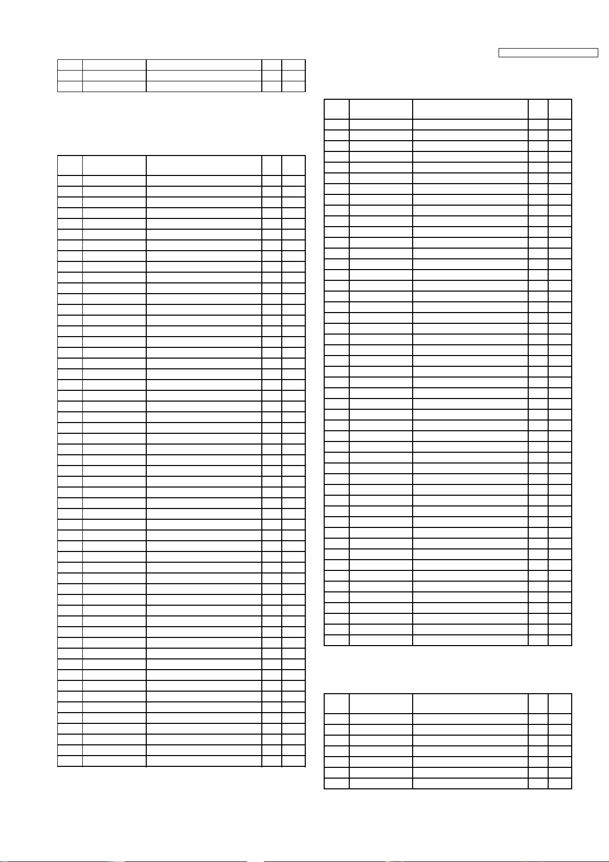
126 CD SOM CD serial data I 0
127 CD SIM CD serial data O 1.4
128 MD1 (Connecting to VDD) - 5.2
Note 1 : Voltage measuerments are with respect to ground,
with a voltmeter (internal resistance : 10M ohms).
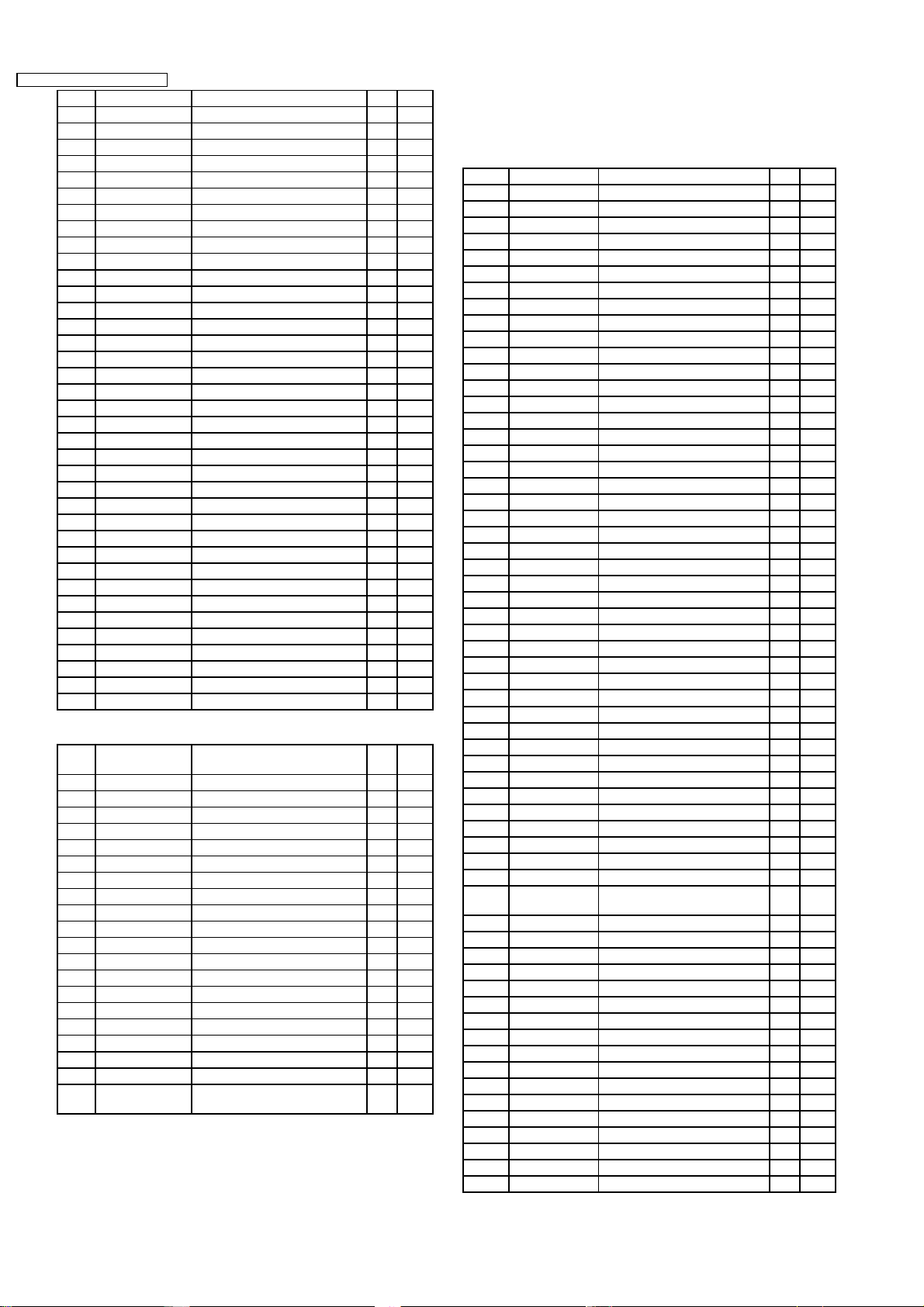
IC901 : C2BBGD000016
Pin
No.
1 MSM MS gain control O 0
2,3 - No connection - -
4 VSSI Ground - 0
5 RX0 Communication data I 5.2
6 RX1 (+5V pull-up) - 5.2
7 VDDI +5V power supply - 5.2
8 RDI CAN-BUS data I 4.9
9 SCLK Not used - -
10 TDO CAN-BUS data O 0
11-13 - No connection - -
14 IF+C IF count I 4.8
15 ANT+ Motor antenna control I 0
16 - No connection - 17 VRL (Connecting to ground) - 0
18 VRH (Connecting to VDD) - 5.2
19 AMP+ Ext. Amp power I 4.9
20 VDD +5V power supply - 5.2
21 +BMONI +B monitor I 3.0
22 SP-L SP Lch level detection I 3.0
23 SP-R SP Rch level detection I 3.1
24 P-ANT Antenna short detection I 1.8
25 - No connection - 26 CANE (Connecting to VDD) - 5.2
27 VPP (Connecting to VDD) - 5.2
28 OSC1 Crystal oscillator - 1.8
29 OSC2 Crystal oscillator - 2.7
30 /RESET Reset input I 0
31 IRQ (CAN-BUS data) I 4.9
32,33 - No connection - 34-36 - (Connecting to ground) - 0
37 MODE C Audio mode selection O 4.9
38 MODE B Audio mode selection O 0
39 MODE A Audio mode selection O 0
40 SP CONT Speaker control O 0
41 WAKE OUT CAN BUS request O 5.2
42 PA2 (NERR) Error/Time out signal I 0
43 PA1 (STB) Data strobe O 0
44 PA0 (EN) Chip enable O 0
45 TX0 Communication data O 5.2
46 TX1 Not used - 0
47 - No connection - -
48 T-RDI CAN-BUS data I 4.8
49 T-TDO Not used - -
50 T-SCLK Not used - -
51 AS-C Speaker out mute O 5.1
52 AS-B Speaker out mute O 5.1
53 AS-A Speaker out mute O 5.1
54-57 - No connection - -
58 VSS Ground - 0
59 M2F Tape main motor control O 0
60 MS Tape MS mode control O 4.9
61 F/R Tape F/R control O 4.9
62 EQ Metal tape select O 4.9
63 NRSW Dolby mode selection O 0.3
64 - No connection - -
Port Description I/O (V)
AUDI / CQ-JA1920L / CQ-JA1924L
9.2. DSP Block
IC801 : YEAMAK7712AF
Pin
No.
1 TSTI Not used - -
2-4 - (Connecting to ground) - 0
5 /PD (Connecting to VDD) - 5.0
6 /RST Reset input I 0
7-9 - Not used - 10,11 DVB +5V power supply - 5.0
12-19 - Not used - -
20 SMODE (Connecting to VDD) - 5.0
21-23 - Not used - -
24 DVDD +5V power supply - 5.0
25 DVSS Ground - 0
26 XTI Crystal oscillator - 2.6
27 XTO Crystal oscillator - 2.4
28 TSTI2 (Connecting to VDD) - 5.0
29 /CS DSP chip select I 5.2
30 /WRQ DSP data write request I 5.2
31 DVSS Ground - 0
32 DVDD +5V power supply - 5.0
33 SCLK DSP clock I 5.2
34 SI DSP serial data I 0
35 WRDY DSP write ready O 0
36 DRDY DSP write ready O 0
37 SO DSP serial data O 0
38-48 - Not used - -
49 DVSS Ground - 0
50 DVDD +5V power supply - 5.0
51-68 - Not used - -
69 DVSS Ground - 0
70 DVDD +5V power supply - 5.0
71,72 Ground - 0
73 DVDD +5V power supply - 5.0
74,75 DVB +5V power supply - 5.0
76-78 - Not used - -
79 AVB +5V power supply - 5.0
80,81 AOUT R2,L2 Audio-Rear output O 2.5
82 NC No connection - 83,84 AOUT R1,L1 Audio-Front output O 2.5
85,86 Ground - 0
87,88 +5V power supply - 5.0
89 NC No connection - -
90 AINR- Audio Rch (-) input I 2.3
91 AINR+ Audio Rch (+) input I 2.5
92 AINL- Audio Lch (-) input I 2.3
93 AINL+ Audio Lch (+) input I 2.5
94 VCON Voltage control - 2.5
95,96 Ground - 0
97 AVDD +5V power supply - 5.0
98,99 +5V power supply - 5.0
100 NC No connecion - -
Port Description I/O (V)
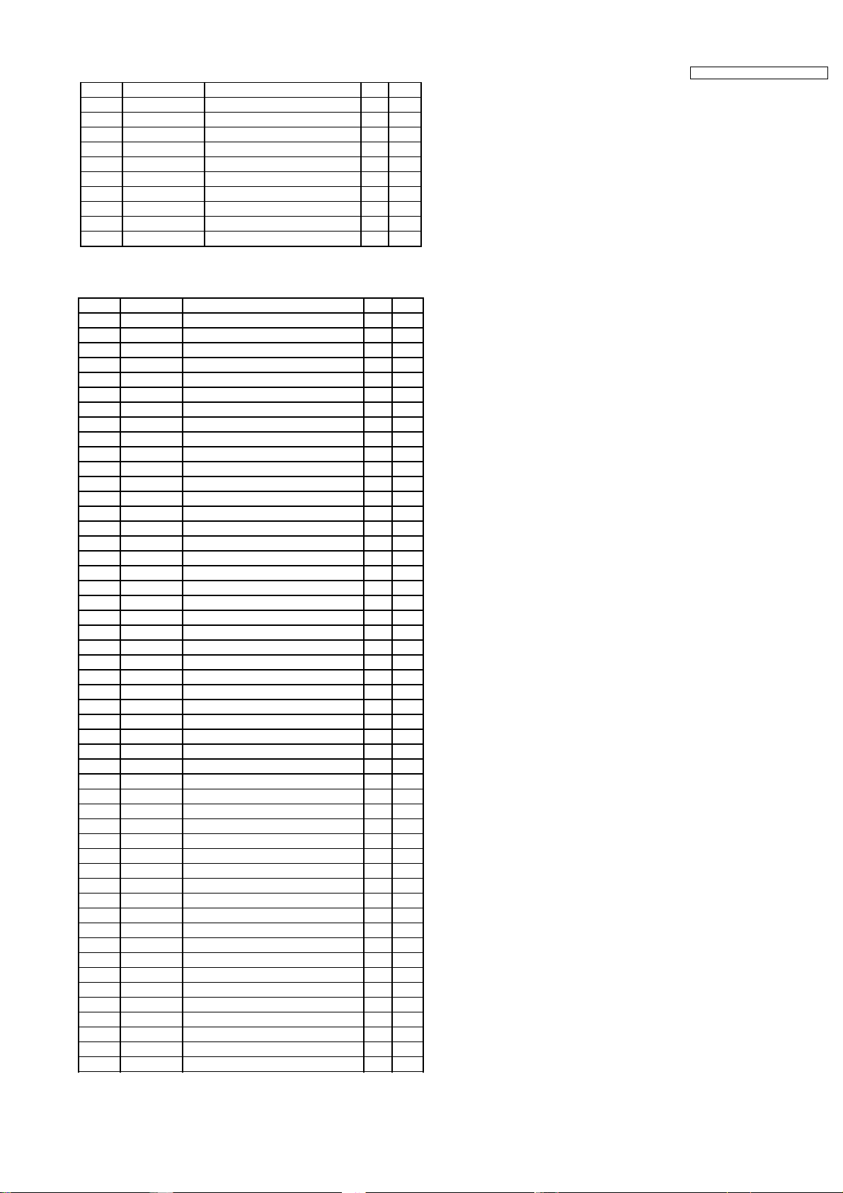
9.3. Display Block
IC611 : C2BBFE000091
Pin
No.
1-8 - Not used - -
9 GND Ground - 0
10,11 - Not used - -
12 TUNE.UP Tune up switch I 0
13 TUNE.DOWN Tune down switch I 0
14 VOL.UP Volume up switch I 5.0
15 VOL.DWN Volume down switch I 0
Port Description I/O (V)
9
AUDI / CQ-JA1920L / CQ-JA1924L
16 TUNE.PUSH Tune push switch I 5.0
17 - No connection - -
18-23 D0-5 LCD control data O 0
24 GND Ground - 0
25,26 D6,7 LCD control data O 0
27 SCAN.LED SCAN LED on/off O 10.2
28 P.SCAN.LED P.SCAN LED on/off O 10.2
29 RBDS.LED RBDS LED on/off O 0
30 RANDOM.LED RANDOM LED on/off O 0.4
31 E LCD driver enable O 0
32 ILL 1 Illumination control O 0
33 ILL 2 Illumination control O 0
34 RESET LCD reset O 0
35 RESET Reset input I 4.7
36 KI1 Key data I 0
37 LED.DATA LED control data O 0
38 LED.CLK LED control clock O 0
39 LED.R.CLK LED control clock O 0
40 VDD +5V power supply - 5.2
41 X2 Crystal oscillator - 3.0
42 X1 Crystal oscillator - 1.7
43 IC (Connecting to ground) - 0
44 - No connection - 45 KI2 Key data I 0
46 AVSS Ground - 0
47 PHOTO.IN Photo sensor data I 0
48,49 KO2,1 Key scan O 0
50-53 KI3-6 Key data I 0
54 AO LCD driver select O 0
55 AVDD +5V power supply - 5.2
56 AVREF +5V power supply - 5.2
57 PANEL.SI Serial data for panel I 5.1
58 PANEL.SO Serial data for panel O 0
59 PANEL.CLK Clock for panel I 5.0
60,61 KO3,4 Key scan O 0
62 K-LINE IN K-line data I 5.2
63 K-LINE OUT K-line data O 5.2
64 KO5 Key scan O 0
IC612 : YEAMNJU64 50G
Pin
No.
1,2 COM7,8 LCD common signal O 0.1
3-10 - No connection - -
11-70 SEG59-0 LCD segment data O 0.1
71 AO LCD driver select I 0
72 OSC1 Oscillator terminal - 1.9
73 OSC2 Oscillator terminal - 2.0
74 E LCD driver enable I 0
75 R/W (Connecting to ground) - 0
76 GND Ground - 0
77-84 D0-7 LCD control data I 0
85 P.ON.5V +5V power supply - 4.9
86 RESET Reset input I 5.2
87 - No connection - -
88 V5 Reference voltage setting - -4.7
89 V3 Reference voltage setting - -0.8
90 V2 Reference voltage setting - 1.1
91 M/S (Connecting to +5V) - 4.9
92 V4 Reference voltage setting - -2.8
93 V1 Reference voltage setting - 3.0
94-
100
Port Description I/O (V)
COM0-6 LCD common signal O 0.1
9.4. CD Servo Block
IC401 : YEAMCXD2597Q
Pin No. Port Description I/O (V)
1 SQSO Sub Q-cord data O 0.5
2 SQCK Sub Q-cord read clock I 4.9
3 XRST System reset I 4.9
4 SYSM Mute input I 4.9
5 DATA Serial data I 3.4
6 XLAT Serial data latch I 4.9
7 CLOK Data shift clock I 4.0
8 SENS SENS output O 0.8
9 SCLK SENS read clock I 5.1
10 VDD +5V power supply - 4.9
11 ATSK Anti-shock signal I/O 0
12 SPOA (Connecting to ground) - 0
13 SPOB (Connecting to ground) - 0
14 XLON Access mode selection O 4.4
15 WFCK Not used - 16 XUGF XUGF output O 0
17 XPCK XPCK output O 0
18 GFS GFS output O 4.1
19, 20 - Not ised - -
21 COUT Track count I/O 0
22 MIRR Mirror signal I/O 0
23 DFCT Defect signal I/O 0
24 FOK Focus OK signal I/O 4.5
25 LOCK GFS sampling status I/O 4.5
26 MDP Spindle motor control O 2.5
27 SSTP (Connecting to ground) - 0
28 SFDR Sled drive O 1.1
29 SRDR Sled drive O 0
30 TFDR Tracking drive O 0
31 TRDR Tracking drive O 0
32 FFDR Focus drive O 0
33 FRDR Focus drive O 0.4
34 VSS Ground - 0
35-37 - (Connecting to ground) - 0
38 VC Middle point voltage input I 2.3
39 FE Focus error I 2.6
40 SE Sled error I 2.0
41 TE Tracking error I 2.2
42 RFDC RF signal I 3.2
43 AVSS0 Ground - 0
44 IGEN OP-amp constant-cu rrent input I 2.3
45 AVDD0 +5V power supply - 4.9
46 ASYO EFM full-swing output O 1.6
47 ASYI asymmetrical comparison
voltage
48 BIAS asymmetric al constant-current I 2.4
49 RFAC EFM signal input I 2.3
50 AVSS3 Ground - 0
51 CLTV VCO1 control voltage I 2.3
52 FILO PLL filter O 0
53 FIFI PLL filter I 1.8
54 PC0 PLL charge-pump O 1.8
55 AVDD3 +5V power supply - 4.9
56 VCTL VCO2 control voltage I 2.4
57 VPCD EFM PLL charge-pump O 2.5
58 VSS Ground - 0
59 VDD +5V power supply - 4.9
60-64 - Not used - -
65 XVDD Power supply for master clock - 4.9
66 XTAI Crystal oscillator - 1.7
67 XTAO Crystal oscillator - 3.9
68 XVSS Ground - 0
I 2.6
10
69 AVDD1 +5V power supply - 4.9
70 AOUT1 Lch audio output O 2.0
71 AIN1 Lch OP-amp input I 2.0
72 LOUT1 Lch line-out O 2.0
73 AVSS1 Ground - 0
74 AVSS2 Ground - 0
75 LOUT2 Rch line-out O 2.0
76 AIN2 Rch OP-amp input I 2.0
77 AOUT2 Rch audio output O 2.0
78 AVDD2 +5V power supply - 4.9
79, 80 - Not used - -
IC451 : C2BBFC000021
Pin No. Port Description I/O (V)
1 NC No connection - 2 SQSO Sub Q-cord data I 0.5
3 CLKOFF LSI clock stop O 5.0
4 SCKM Data shift clock O 5.0
5 MUTE Analog mute O 0
6 SOM Serial data O 0
7 PLLOFF Not used - 8 SIM Serial data I 1.5
9 TNNER Inner switch I 4.4
10 OUT Disc-out detection I 4.2
11 IN Disc-in detection I 4.2
12 CLAMP Disc clamp detection I 0
13 PC0 Spindle motor driver on/off I/O 0
14 PC2 Loading motor driver on/off I/O 5.1
15 VREF +5V power supply - 5.1
16,17 NC No connection - -
18 XIN Crystal oscillator - 1.8
19 XOUT Crystal oscillator - 2.6
20 NC No connection - 21 AVSS Ground - 0
22 VSS Ground - 0
23 VCC +5V power supply - 5.1
24 NC (Connecting to ground) - 0
25 XCIN Not used - 26 LOCK Spindle PLL lock detection I 4.5
27 NC No connection - 28 /RST CPU reset I 4.8
29 NC No connection - 30 CDON CPU operation enable I 0
31 ATSK Anti-shock signal I 0
32 FOK RF level detection I 4.5
33 MIRR Mirror signal detection I 0
34 ATSK Anti-shock signal I 0
35 LOD Loading motor control I/O 2.3
36 PC1 Actuator motor drive on/off I/O 0
37 MODE Access mode selection O 0
38 SCLK SENS read clock O 5.1
39 SENS Servo LSI status I 0.7
40 CLOK Servo LSI data shift clock O 4.1
41 XLAT Serial data latch O 5.0
42 DATA Serial data O 3.5
43 SYSM LSI mute O 0
44 NC No connection - 45 CDON Not used - 5.0
46- 49 - Not used - -
50 /RST Not used - 4.8
51 VSS Ground - 0
52 P53 Not used - 53 XRST Servo LSI reset O 5.1
54 SQCK Sub Q-cord read clock O 5.1
55,56 - Not used - -
AUDI / CQ-JA1920L / CQ-JA1924L
11
 Loading...