

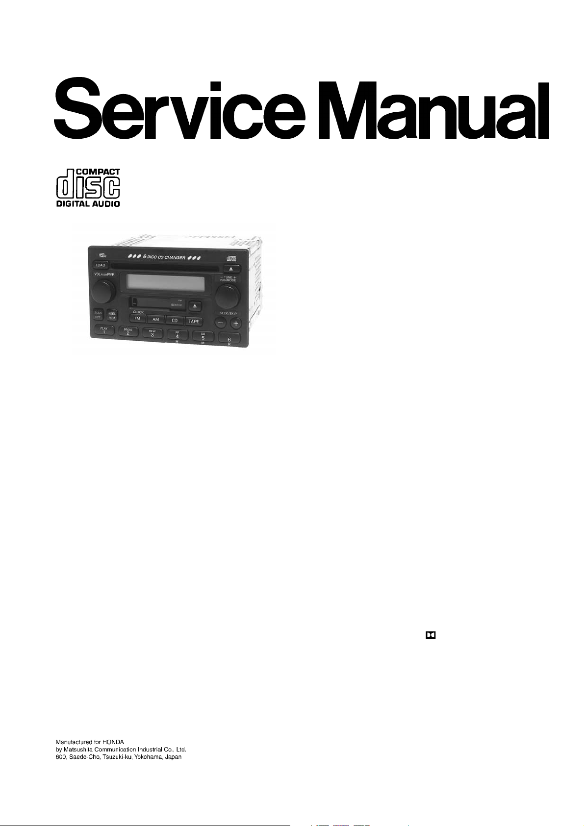
Panasonic CQEH-8160-AK Service manual
ORDER No.0159
AUTOMOTIVE ELECTRONICS
HONDA
CQ-EH8160AK
AM/FM MPX ELECTRONIC TUNING
RADIO with Stereo Cassette Tape
Player and 6-Disc CD Changer
HONDA PART No. : 39100-S9A-A200
ID CORD : 1TN0
VEHICLE : CR-V
DESTINATION : North America
PRODUCED AFTER : Feb., 2002
I0
Specification*
General
Power Supply DC 12V (11V - 16V),
Test Voltage 13.2V
Negative Ground
Current Consumption Less than 3.0A (at 0.5W)
Power Output 30W×4
Output Impedance 4Ω
AM Radio
Frequency Range 530 - 1,710kHz
Usable Sensitivity 24dB/µV (S/N 20dB)
FM Stereo Radio
Frequency Range 87.7 - 107.9MHz
Usable Sensitivity 6dB/µV (S/N 30dB)
Cassette Player
Reproduction System 4-Track, 2-Program Stereo
Tape Speed 4.76cm/sec.
Wow and Flutter Less than 0.2% (WRMS)
Signal to Noise Ratio More than 38dB (IHF-A)
IDC
Signal to Noise Ratio More than 63dB (IHF-A)
Total Harmonic Distortion Less than 0.4%
Channel Separation More than 50dB (IHF-A)
Dimensions** (W×H×D) 180×102×170mm
Weight** 2.4kg
* Specifications and the design are subject to possible modification
without notice due to improvements.
** Dimensions and Weight shown are approximate.
Dolby noise reduction manufactured under license from Dolby
Laboratories Licensing Corporation.
“Dolby” and the double-D symbol
Laboratories Licensing Corporation.
are trade marks of Dolby
HONDA / CQ-EH8160AK
CONTENTS
Page Page
1 FEATUERS 2
2 LASER PRODUCTS
3 REAR VIEW
4 FRONT VIEW AND FUNCTIONS
5 WIRING CONNECTIONS
6 BLOCK DIAGRAM (Main, Display, Tape Block)
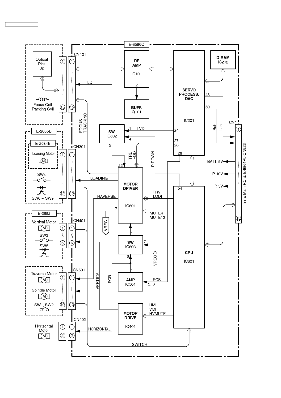
7 BLOCK DIAGRAM (CD Servo Block)
8 TERMINALS DESCRIPTION
9 ALIGNMENT INSTRUCTIONS
10 ALIGNMENT POINTS
11 CD DISC CENTERING ALIGNMENT
12 PACKAGE AND IC BLOCK DIAGRAM
13 REPLACEMENT PARTS LIST 17
2
14 EXPLODED VIEW (Unit)
2
15 CD CHANGER PARTS LIST
16 EXPLODED VIEW (CD Deck-1)
3
4
17 EXPLODED VIEW (CD Deck-2)
5
18 EXPLODED VIEW (CD Deck-3)
19 TAPE PLAYER PARTS
6
7
20 EXPLODED VIEW (Tape Deck)
10
21 WIRING DIAGRAM
22 SCHEMAT IC DIAGRAM (1)
10
11
23 SCHEMAT IC DIAGRAM (2)
12
23
24
27
28
29
30
32
33
40
41
1 FEATUERS
·
PLL (Phase Locked Loop) synthesized tuning.
·
18-station preset (12-FM, 6-AM).
·
Automatic preset setting.
·
6-Disc CD changer (in dash board).
·
Dolby noise reduction.
·
Adjustable VOL, BAS, TRE, FAD and BAL.
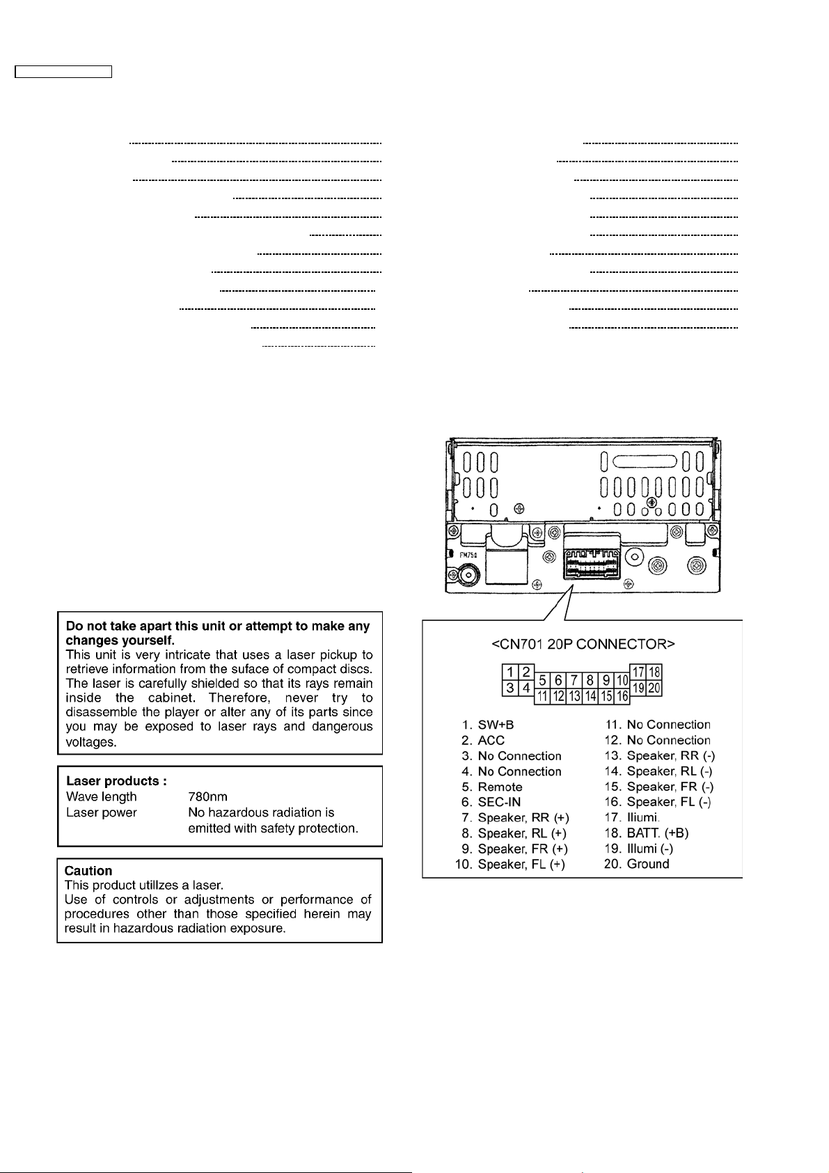
2 LASER PRODUCTS
3 REAR VIEW
2
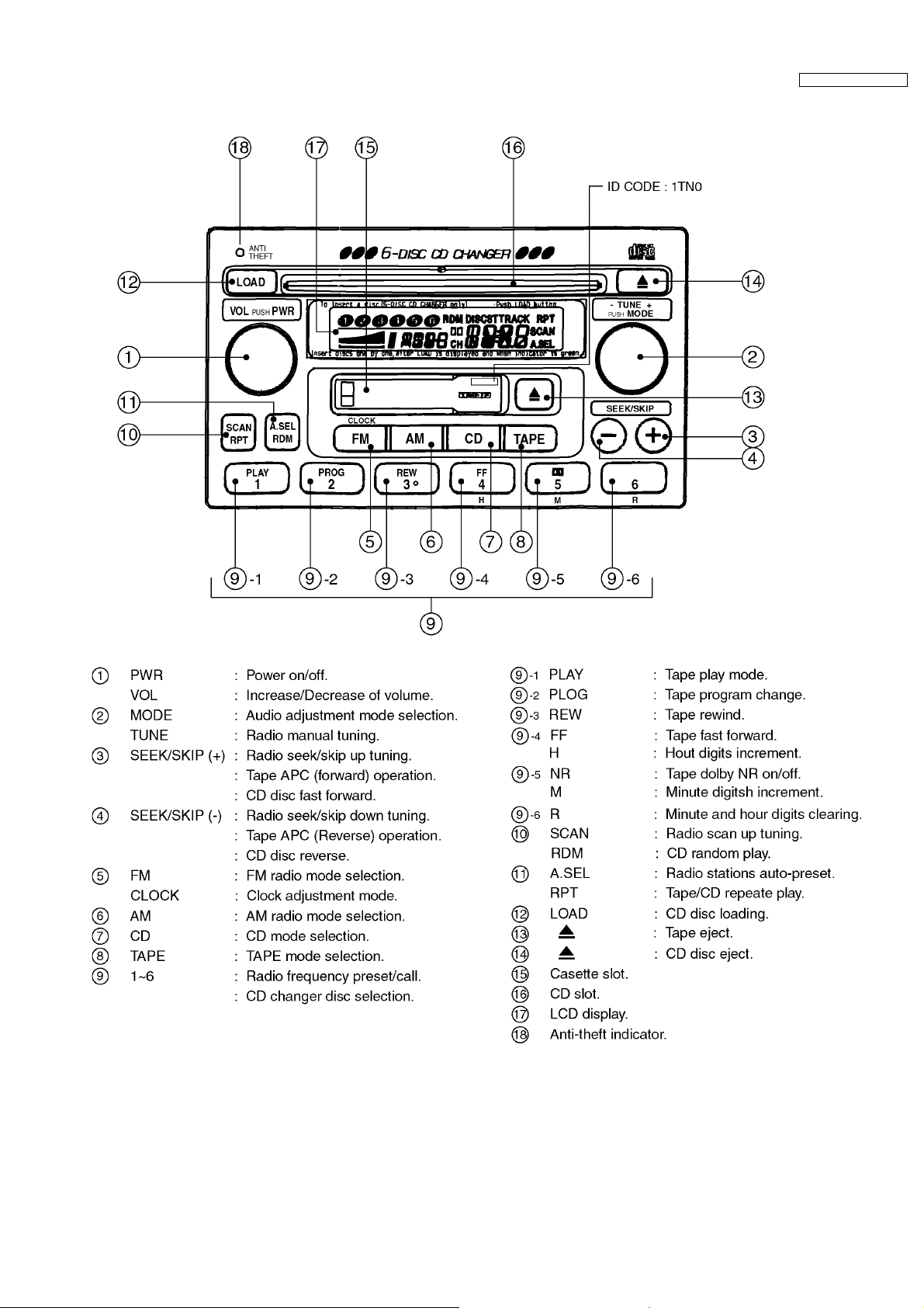
4 FRONT VIEW AND FUNCTIONS
HONDA / CQ-EH8160AK
3
HONDA / CQ-EH8160AK
5 WIRING CONNECTIONS
4
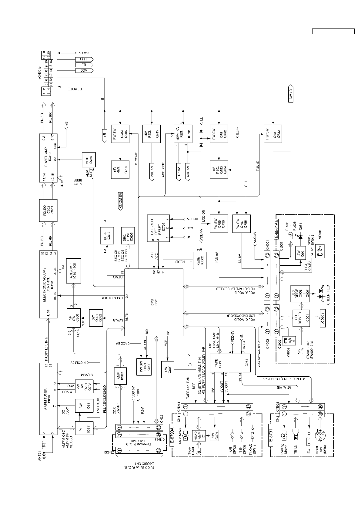
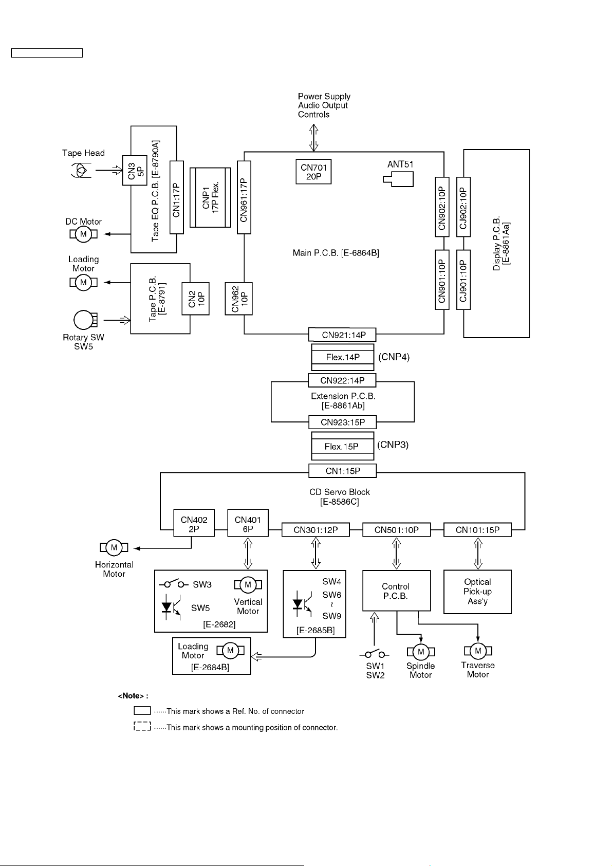
6 BLOCK DIAGRAM (Main, Display, Tape Block)
HONDA / CQ-EH8160AK
5
HONDA / CQ-EH8160AK
7 BLOCK DIAGRAM (CD Servo Block)
6
8 TERMINALS DESCRIPTION
HONDA / CQ-EH8160AK
8.1. Main Block
IC601 : C2CBHG000077
Pin
No.
1 BEEP Beep output O 0
2 IDC-ST/SP CD.C start/stop O 4.9
3 EVOL CLK Electronic volume clock O 0
4 EVOL DATA Electronic volume data O 0
5 SEC-LED Security LED on/off O 4.9
6 VOL A Rotary encoder data I 0.5
7 VOL B Rotary encoder data I 0.5
8 LCD-CLK Shift clock for LCD data O 0
9 LCD-DI LCD data O 5.0
10 LCD-DO LCD data I 0
11 RESET Reset input I 4.9
12 XT2 Crystal oscillator terminal - 2.4
13 XT1 Crystal oscillator terminal - 0.7
14 VSS Ground - 0
15 X2 Crystal oscillator terminal - 2.3
16 X1 Crystal oscillator terminal - 1.8
17 REGOFF (Connecting to VDD) - 4.9
18 REGC (Connecting to VDD) - 4.9
19 VDD +5V power supply - 4.9
20 VOL C Rotary encoder data I 4.8
21 VOL D Rotary encoder data I 0.5
22 LCD-CE LCD driver enable O 0
23 BOSE (Connecting to ground) - 0
24 SEC-CS Security ROM chip select O 0
25 SEC-CLK Data shift clock for security ROM O 0
26 SEC-DI Security data I 0
27 SEC-DO Security data O 0
28 SET-SEC1 (Ground pull-down) - 0
29 SET-TIME2 (Vdd pull-up) - 4.9
30 SET-TIME (Vdd pull-up) - 4.9
31 P.CONT COM8V power switch O 4.8
32 ACC CNT ACC 5V power switch O 4.9
33 STB Power amp. Stand-by O 4.9
34 LCD ON LCD illumi. on/off O 4.9
35 TUNER +B Motor antenna power O 4.9
36 PLL-CE PLL chip select O 0
37 PLL-DO PLL data O 0
38 PLL-CLK Shift clock for PLL data O 0
39 PLL-DI PLL data I 5.0
40 VSS Ground - 0
41 VDD +5V power supply - 4.9
42 AREA (Ground pull-down) - 0
43 ST-IND FM stereo detection I 0.3
44 CA.PON Tape power control O 4.9
45 CM.PON Tape power control O 4.9
46 M2 Main motor control O 0
47 M1A Loading motor control O 0
48 M1B Loading motor control O 0
49 T.IN Tape-in detection I 0
50 MSM MS gain contrl O 4.9
51 A/B Tape side detection I 0
52 M2F Main motor control O 0
53 EQ(MTL) Metal tape mode selection O 4.9
54 F/R Tape head change O 0
55 DOLBY Dolby NR on/off O 4.9
56 T.LOAD Tape loading detection I 0
57 MS(PL/FF) MS mode selection O 0
58 MS MS detection I 0
59 REMO3/4 (Ground pull-down) - 0
60 H.BUSOUT Not used - -
Port Description I/O (V)
61 NAVI-IN (Vdd pull-up) - 4.8
62 NC No connection - 63 NC No connection - 64 NAVI-MUTE Not used - 65 BIT1 Tape mode switch I 4.6
66 END.A Tape end signal I 1.5
67 END.B Tape end signal I 2.4
68 BIT2 Tape mode switch I 4.6
69 EQ Metal/Normal switchl I 0
70 BIT3 Tape mode switch I 0
71 NC No connection - 72 NC No connection - 73 IC/VPP (Connecting to ground) - 0
74 REMO Remote control signal O 5.0
75 SW.A Audio signal switch O 0
76 SW.B Audio signal switch O 0
77 MUTE Not used - 78 NC No connection - 79 NC No connection - 80 VSM Phase diff. level detection I 0.6
81 AMP MUTE Power amp mute O 0
82 AVDD +5V power supply - 4.9
83 AVREF1 Analog reference voltage I 5.0
84 AVSS Ground - 0
85 NC (Connecting to ground) - 0
86 NC No connection - 87 ACC-DET ACC level detection I 4.5
88 TAPE EJ Tape eject SW I 4.6
89 H.BUS.IN Not used - 4.8
90 GAIN (+5V pull-up) - 4.8
91 IDCEJECT CD disc eject SW I 4.7
92 BAT-DET Battery level detection I 4.5
93 EJ.INH Tape/Disc eject SW I 4.4
94 IDC-SI CD.C serial data O 4.0
95 RXO Not used - 0
96 TXO Not used - 4.9
97 IDC-CLK Shift clock for CD.C data O 4.9
98 IDC-SO CD.C data O 1.2
99 CD-RESET CD.C reset O 4.9
100 CDON CD.C controller enable O 4.9
Note :
Voltage measuerments are with respect to ground, with a
voltmeter (Internal resistance : 10M ohms.)
8.2. Display Block
IC901 : YEAMLC75853
Pin
No.
1, 2 S1, 2 Disc LED on/off O 0
3 S3 Not used - -
4-40 S4-40 LCD segment data O 2.5
41-43 COM1-3 LCD common O 2.5
44 S41 LCD segment data O 2.5
45-49 KS2-6 Key strobe O 0.9
50-53 KI1-4 Key data I 0
54 KI5 (Connecting to ground) - 0
55 TEST (Connecting to ground) - 0
56 VDD +5V power supply - 5.1
57 VDD1 LCD angle - 3.3
58 VDD2 LCD angle - 1.7
59 VSS Ground - 0
60 OSC Oscillator terminal - 3.9
Port Description I/O (V)
7
HONDA / CQ-EH8160AK
61 DO Key data output O 4.1
62 CE LCD driver chip enable I 0
63 CL Shift clock for LCD data I 0
64 DI LCD data input I 0
8.3. CD Servo Block
IC201 : MN662783RPW
Pin
No.
1 VDD +5V power supply - 5.0
2 D0 D-RAM data I/O 2.3
3 D1 D-RAM data I/O 1.8
4 /WE D-RAM data write O 4.9
5 /RAS D-RAM row address strobe O 3.4
6 D2 D-RAM data I/O 0.8
7 D3 D-RAM data I/O 0
8 /CAS0 D-RAM columun address strobe O 3.9
9 /CAS1 D-RAM columun address strobe O 0
10 A8 D-RAM address O 0.6
11 A7 D-RAM address O 1.1
12 A6 D-RAM address O 0.7
13 A5 D-RAM address O 0
14 A4 D-RAM address O 1.1
15 A9 D-RAM address O 0.4
16 A0 D-RAM address O 1.0
17 A1 D-RAM address O 1.0
18 A2 D-RAM address O 1.0
19 A3 D-RAM address O 0
20 VSS2 Ground - 0
21 VDD2 +5V power supply - 5.0
22,23 - Not used - -
24 TVD Traverse motor control O 2.5
25 PC Not used - 26 ECS Spindle motor control O 2.4
27 TRD Tracking coil drive O 2.5
28 FOD Focus coil drive O 2.4
29 FBAL Focus balance O 1.9
30 TBAL Tracking balance O 3.0
31 VREF Reference voltage I 2.5
32 FE Focus error I 2.5
33 TE Tracking error I 2.5
34 RFENV RF envelope I 2.5
35 OFT Off track signal I 0
36 /RFDET RF detecting signal I 0
37 BDO Drop-out signal I 0
38 LDON Laser on signal O 4.5
39 ARF RF signal I 2.5
40 IREF Reference current input I 1.2
41 DRF Biase for DSL I 2.4
42 DSLF Loop filter for DSL I/O 2.5
43 SDLF2 Loop filter for DSL I/O 2.2
44 PLLF Loop filter for PLL I/O 1.4
45 VCOF Not used - 46 AVDD2 +5V power supply - 5.0
47 AVSS2 Ground - 0
48 OUTL L channel output O 2.3
49 AVSS1 Ground - 0
50 OUTR R channel output O 2.3
51 AVDD1 +5V power supply - 4.7
52-54 - (Connecting to ground) - 0
55 FLAG Flag output O 0
56 FCLK Frame clock O 0
57-59 - Not used - -
60 TX Not used - 61 MCLK Clock for I/F command I 1.0
Port Description I/O (V)
62 MDATA Data for I/F command I 3.1
63 MLD I/F command load I 5.0
64 BLKCK Subcode block clock O 0
65 SQCK Ext. clock for sub code-Q I 5.0
66 SUBQ Code for sub. code-Q O 3.8
67 DMUTE Mute input I 0
68 STAT Status signal O 5.0
69 /RST Reset input I 5.0
70 CSEL (Connecting to ground) - 0
71 PMCK PM clock O 2.5
72 SMCK SM clock O 2.5
73 SUBC Serial data of sub code O 0
74 SBCK Shift clock for SUBC I 0.6
75 /CLDCK Not used - 76 /TEST (Connecting to VDD) - 5.0
77 X1 Crystal oscillator - 0.4
78 X2 Crystal oscillator - 3.2
79 VDD1 +5V power supply - 5.0
80 VSS1 Ground - 0
IC301 : MN1873260AB4
Pin
No.
1 VDD +5V power supply - 5.0
2 OSC2 Crystal oscillator - 2.2
3 OSC1 Crystal oscillator - 2.1
4 VSS Ground - 0
5 XI (Connecting to ground) - 0
6 XO Not used - 7 CM (Connecting to ground) - 0
8 VREFH Reference voltage I 5.0
9 SW13 Shuter SW I 4.9
10 SW12 Horizontal origin I 4.9
11 SW11 Clump SW I 0
12 SW10 Play SW I 0
13 SW4 Shuter SW I 4.9
14 SW3 Tray origin SW I 0
15 SW2 Inner SW I 4.8
16 SW1 Outer SW I 4.9
17 VREFL Reference voltage I 0
18 /RESET Reset input I 4.9
19 - (Ground pull-down) - 0
20 SCKM Clock for serial data I 5.0
21 SIM CD changer serial data I 1.3
22 SOM CD changer serial data O 4.3
23 SQCK Ext. clock for sub. code-Q O 5.0
24 SUBQ Code for sub. code-Q I 1.6
25 - Not used - 5.0
26 - (Ground pull-down) - 0
27 CD.ON CD changer start/stop I 5.0
28 - Not used - 5.0
29 BLKCK Sub. code block clock I 0
30 P.ON Not used - 5.0
31 MUTE Mute output O 5.0
32 - (Ground pull-down) - 0
33 SENS Servo status O 0
34 CLVS Servo status O 5.0
35 FLOCK Focus servo lock O 0.2
36 TLOCK Tracking servo lock O 0
37 VMI Horizontal motor control O 2.5
38 HMI Vertical motor control O 0
39 HVMUTE H/V motor mute O 0
40-42 - (Ground pull-down) - 0
43 SW9 Disc-in (B) SW I 0
44 SW8 Disc-in (L) SW I 0
45 SW7 Disc-in (F) SW I 0
46 SW6 Disc push SW I 0
Port Description I/O (V)
8

47 SW5 Tray hight SW I 4.5
48 BDO Drop-out signal I 0
49 DQSY Not used - 50 /RST Reset output O 5.0
51 STAT Status signal I 2.1
52 DMUTE Mute output O 0
53 XE Not used - 54 P.DOWN Power down signal O 0
55 - No connection - 56 MLD I/F command load O 5.0
57 MDATA Data for I/F command O 3.1
58 MCLK Clock for I/F command O 4.1
59 SPMT Spindle mute O 5.0
60 MUTE12 Focus/Tracking mute O 0
61 MUTE4 Loading motor mute O 4.8
62 LDOI Loading motor control I/O 2.5
63 TRV Forced traverse control I/O 2.4
64 SYNC Not used - -
HONDA / CQ-EH8160AK
9
HONDA / CQ-EH8160AK
9 ALIGNMENT INSTRUCTIONS
9.1. Alignment Conditions
·
Power Supply Voltage : DC13.2V
·
Output Impedance : 4
·
Output Power : 0.5W
Note :
Do not align the FM/AM package block. When the package block is necessary, it will be supplied already aligned at the
factory.
Ω
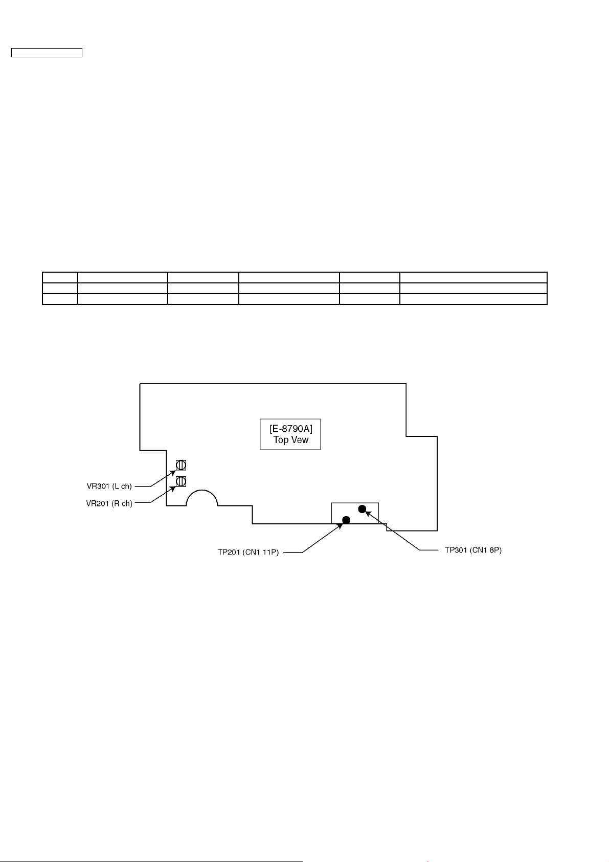
9.2. Dolby NR Alignment
Step Alignment Item Test Tape VTVM Connection Adjust Remarks
(1) DOLBY NR Rch RFKZ0038 TP201 VR201 Adjust for 388mV ±1.0dB
(2) DOLBY NR Lch RFKZ0038 TP301 VR301 Adjust for 388mV ±1.0dB
10 ALIGNMENT POINTS
·
Balance, Fader Control : center
·
Bass, Treble Control : Center
·
Dolby NR: OFF
10
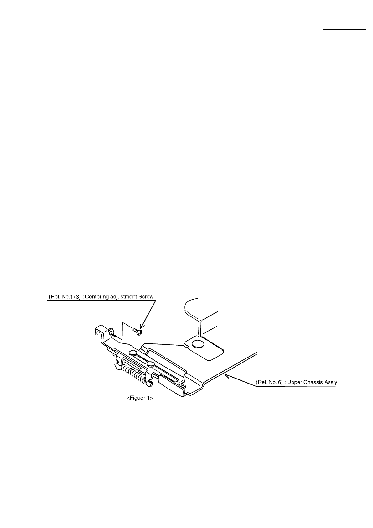
11 CD DISC CENTERING ALIGNMENT
·
This adjustment is for assuring that compact discs will be placed in the center of the turntable.
<Adjustment Condition / Jig>
·
Power Supply Voltage : 13.2V
·
Test Disc : TCD-792A
<Adjustment Procedures>
1. Attach the adjusting screw to the upper chassis (See Figure 1.).
2. Insert the test CD (TCD-792A) into the disc No.1 position and play it.
3. After checking whether the disc is centered on the turntable, turn the adjusting screw unit it is in the center.
<Check Items>
·
Check that the disc is correctly centered.
·
Check that the disc is securely clamped.
·
Check that no abnormal noise is produced when clamping the disc.
HONDA / CQ-EH8160AK
[Directions of Turning the Adjusting Screw]
·
CD stops before its proper position : Turn the screw counterclockwise.
·
CD overruns : Turn the screw clockwise.
4. After the adjustment, lock the screw.
11
HONDA / CQ-EH8160AK
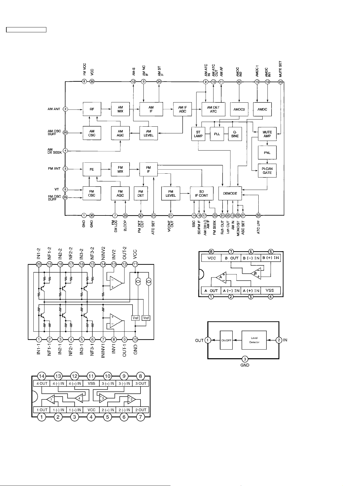
12 PACKAGE AND IC BLOCK DIAGRAM
12.1. Main Block
IC202,203 : YEAMM5243FT1
PK50 : YEP0PTA5 14B0
IC305,612,921 : C0ABBB000179
IC602 : MN1382KTX
IC301,304 : C0ABCB000038
12
 Loading...