

Panasonic CQDPX-172-U Service manual
Specifications*
ORDER No. ACED020274C1
C4
AUTOMOTIVE CONSUMER ELECTRONICS
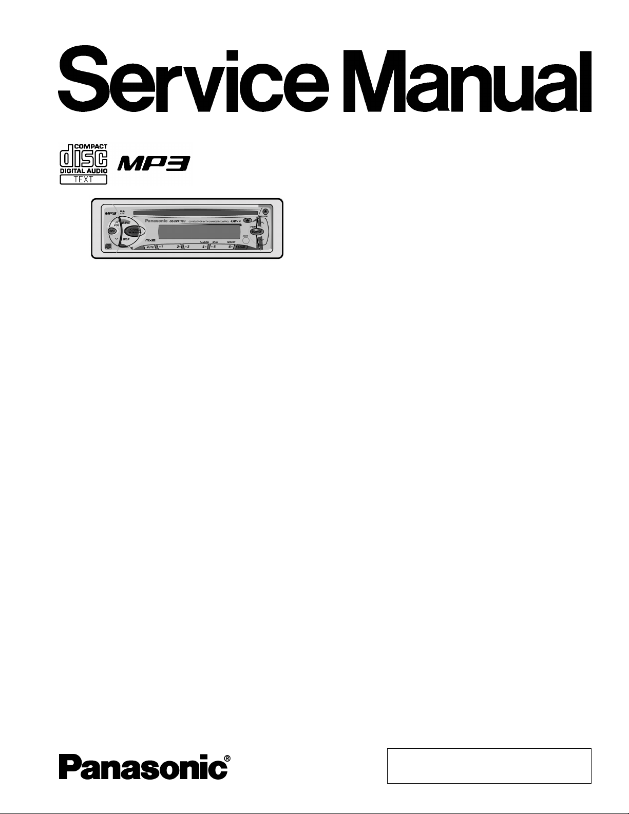
CQ-DPX172U
Removable Front Panel MP3 CD Player
/ Receiver with Changer Control
General
Power Supply DC 12V (11V - 16V),
Test Voltage 14.4V
Negative Ground
Tone Adjustment Range Bass ; ±12dB at 100Hz
Treble ; ±12dB at 10kHz
Current Consumption Less than 2.2A (CD play mode,
0.5W×4ch)
Maximum Power Output 45W×4ch (at 1kHz, Vol. Max.)
Suitable Speaker Impedance 4-8Ω
Pre-AMP Output Voltage 2V (CD play mode; 1kHz, 0dB)
Output Impedance 200Ω
FM Stereo Radio
Frequency Range 87.9 - 107.9MHz
Usable Sensitivity 11.0 dBf (1.25µV, 75Ω)
AM Radio
Frequency Range 530 - 1,710kHz
Usable Sensitivity 28dB/µV (25µV, S/N 20dB)
Wavelength 780nm
Frequency Response 20Hz to 20,000Hz (±1dB)
Signal to Noise Ratio 96dB
Wow and Flutter Below measurable limits
Channel Separation 75dB
Dimensions** 7”×1 15/16”×5 7/8”
(178×50×150mm)
Weight** 3lbs. 5oz (1.5kg)
* Specifications and the design are subject to possible modification
without notice due to improvements.
** Dimensions and Weight shown are approximate.
Avobe specifications comply with EIA standards.
CD Player
Sampling Frequency 32 times over sampling
Pick-Up Type Astigma 3-beam
Light Source Semiconductor Laser
© 2002 Matsushita Communication Industrial Co.,
Ltd. All rights reserved. Unauthorized copying and
distribution is a violation of law.
CQ-DPX172U
CONTENTS
Page Page
1 FEATUERS 2
2 REPLACEING THE FUSE
3 MAINTENANCE
4 NOTES
5 DIMENSIONS
6 LASER PRODUCTS
7 WIRING CONNECTION
8 BLOCK DIAGRAM
9 TERMINALS DESCRIPTION
10 PACKAGE AND IC BLOCK DIAGRAM 7
11 REPLACEM ENT PARTS LIST
2
2
12 EXPLODED VIEW (Unit)
2
13 CD PLAYER PARTS
14 EXPLODED VIEW (CD Deck)
2
2
15 PACKING PARTS LIST
3
16 WIRING DIAGRAM
17 SCHEMAT IC DIAGRAM -1
4
5
18 SCHEMAT IC DIAGRAM -2
10
15
16
17
18
19
24
25
1 FEATUERS
·
PLL (Phase Locked Loop) synthesized tuning.
·
18-FM, 6-AM presets with preset scan
·
Digital servo for reliable CD playback.
·
Removable face plate.
2 REPLACEING THE FUSE
Use fuses of the same specified rating (15A). Using different
substitutes or fuses with higher ratings, or connecting the unit
directly without a fuse, could cause fire or damage to the stereo
unit.
3 MAINTENANCE
Your products is designed and manufactured to ensure a
minimum of maintenance. Use a soft cloth for routine exterior
cleaning. Never use benzine, thinner or other solvents.
4 NOTES
[RADIO BLOCK]
Do not align the AM/FM package block. When the package
block is necessary, it will be supplied already aligned at the
factory.
[CD DECK BLOCK]
This model has no servo alignment points because
microcomputer controls the servo circuit.
5 DIMENSIONS
6 LASER PRODUCTS
2
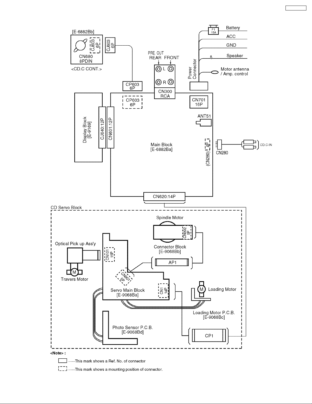
7 WIRING CONNECTION
CQ-DPX172U
3
CQ-DPX172U
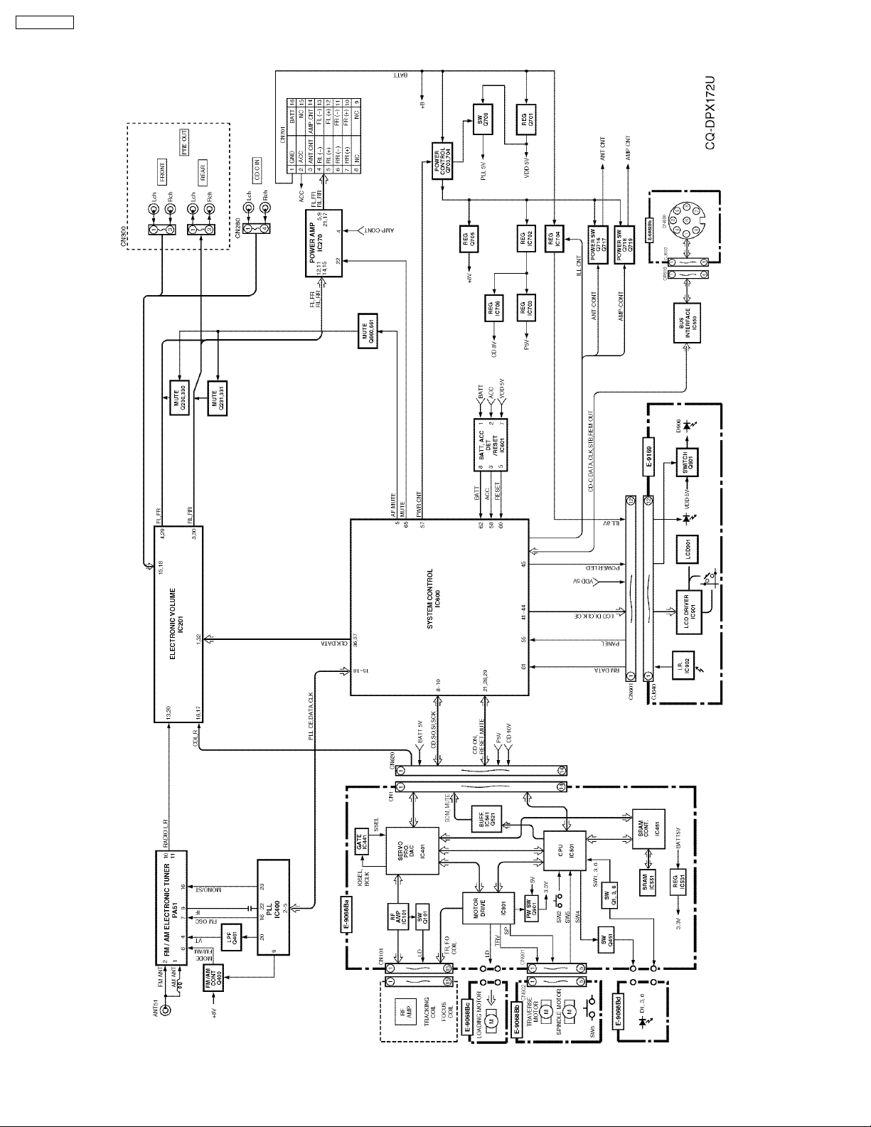
8 BLOCK DIAGRAM
4

9 TERMINALS DESCRIPTION
CQ-DPX172U
9.1. Main Block
IC600 : C2BBGF000292
Pin
No.
1 INIT C Initial C I 4.9
2 NC No connection - 3 NC No connection - 4 AVSS Analog ground - 0
5 AF MUTE AF mute O 5.1
6 AMP.CNT Power Amp. stand-by O 5.0
7 AVREF Reference voltage - 5.1
8 CD-SO CD data I 3.2
9 CD-SI CD data O 3.8
10 CD-SCK CD clock O 5.0
11 CD.C DATA CD changer data O 0
12 NC No connection - 13 CD.C CLK CD changer clock O 0
14 REM OUT CD changer remote cont. data O 5.0
15 PLL CE PLL controller chip enable O 0
16 PLL DATA
17 PLL DATA
18 PLL CLK Clock for PLL O 0
19 NC No connection - 20 NC No connection - 21 CD-RESET CD reset O 5.0
22 NC No connection - 23 NC No connection - 24 NC No connection - 25 NC No connection - 26 NC No connection - 27 NC (GND pull-down) - 0
28 CD-ON CD power on O 5.0
29 CD-MUTE CD mute control I 0
30 CD-SW2 Not used - 31 NC No connection - 32 NC No connection - 33 Vss Ground - 0
34 NC No connection - 35 /ST FM stereo detection I 4.5
36 IC2-CLK Electronic volume clock O 5.0
37 IC2-DATA Electronic volume data I/O 5.0
38 S.LED Not used - 39 NC No connection - 40 BZIN Not used - 41 LCD-DI (MO) LCD data output O 0
42 LCD-DO (MI) LCD data input I 5.0
43 LCD-CLK LCD clock O 0
44 LCD-CE LCD chip enable output O 0.2
45 POWER
46 ANT.CONT Motor antenna control O 0
47 NC No connection - 48 NC No connection - 49 NC No connection - 50 BZOUT Not used - 51 NC No connection - 52 NC No connection - 53 NC No connection - 54 NC No connection - 55 PANEL Panel detect I 4.8
56 CD POWER CD power control O 5.1
57 PWR CNT Power control O 5.1
58 ACC ACC detection I 5.0
Port Description I/O (V)
Data from PLL I 5.1
(MI)
Data for PLL O 0
(MO)
Pilot lamp on O 0
LED
59 RDS DATA Not used - 60 /RESET Reset input I 5.1
61 REM Remocon data input I 5.1
62 BATT Battery detection I 5.0
63 RDS CLK Not used - 64 CD.C.STB (Ground pull-down) I 0
65 MUTE Mute control O 5.1
66 NC (Connecting to ground) - 0
67 VSS0 (Connecting to ground) - 0
68 VDD +5V power supply - 5.1
69 X2 Crystal oscillator - 3.0
70 X1 Crystal oscillator - 1.7
71 VPP (Ground pull-down) - 0
72 NC No connection - 73 NC No connection - 74 VDD0 +5V power supply - 5.1
75 AVREF (Connecting to VDD) - 5.1
76 NC (Connecting to ground) - 0
77 SD Search detect I 5.1
78 INIT D Initial value D I 0
79 INIT A Initial value A I 0
80 INIT B Initial value B I 0
Note 1 : Voltage measuerments are with respect to ground,
with a voltmeter (internal resistance : 10M ohms).
9.2. Display Block
IC901 : YEAMLC75854T
Pin
No.
1-35 SEG9-35 LCD segment O 2.5
36-39 NC No connection - 40-43 COM1-4 LCD common O 2.5
44-49 KS1-6 Key data output O 0.9
50-54 KI1-5 Key data input I 0
55 TEST (Connecting to ground) - 0
56 VDD +5V power supply - 5.1
57 VDD1 Ground through capacitor - 3.3
58 VDD2 Ground through capacitor - 1.7
59 Vss Ground - 0
60 OSC CR oscillator - 3.9
61 DO Key data output O 4.4
62 CE Chip enable I 0
63 CLK LCD clock I 0
64 DI LCD data input I 0
Port Description I/O (V)
5
CQ-DPX172U
9.3. CD Servo Block
IC501 : MN101C28LAC
Pin
No.
1 VREF- Reference voltage for ADC (GND) - 0
2 PA0 (Connecting to GND) - 0
3 PA1 Disc-In sensor I 2.9
4 PA2 Feeder arm SW I 3
5 PA3 Disc-Out sensor I 3
6 PA4 Clamp SW I 0
7 PA5 Inner SW I 3.3
8 PA6 Disc-In sensor I 1.5
9 PA7 Not used - 3.3
10 VREF+ Reference voltage for ADC (+3.3V) - 3.3
11 VDD Power supply (+3.3V) - 3.3
12 OSC2 System clock (7.37MHz) O 1.6
13 OSC1 System clock (7.37MHz) I 1.5
14 VSS Ground - 0
15 XI (Connecting to GND) - 0
16 XO (NC) No connection - 17 MMOD (Connecting to GND) - 0
18 SOM Serial data output O 0.5
19 SIM Serial data input I 0.5
20 SCK Shift clock for serial data I 3
21 SB01/P03 No connection - 22 SUBC CD-TEXT data I 0
23 SBCK CD-TEXT clock O 3.3
24 P06 (NC) No connection - 25 RESET Reset input I 3.3
26 MDATA MPU communication data O 1
27 MCLK Shift clock for MDATA O 2.5
28 SCK Shift clock for serial data I 2.2
29 STAT Servo LSI status I 0
30 TM4IO/P14 No connection - 31 POBF MP3 DSP status I 0
32 DATAREQ MP3 DSP NEXT data request I 3
33 CD. ON CD operation mode I 3.2
34 DQSY CD-TEXT/SUBQ sync. I 0
35 BLKCK BLKCK signal I 3.3
36 SQCK Clock for sub. code data I 1.5
37 SUBQ Sub. code data I 0
38 SBT2/P32 (Connecting to GND) O 0
39 MLD MPU command load O 3.3
40 ACK MP3 DSP acknowledge O 0
41 IOSEL Servo LSI mode setting O 3.3
42 VDD2 Power supply for flash write - 3.3
43 VPP Power supply for flash write - 3.3
44 DSPP0 MP3 DSP data (bit0) I/O 0
45 DSPP1 MP3 DSP data (bit1) I/O 0
46 DSPP2 MP3 DSP data (bit2) I/O 0
47 DSPP3 MP3 DSP data (bit3) I/O 0
48 DSPP4 MP3 DSP data (bit4) I/O 0
49 DSPP5 MP3 DSP data (bit5) I/O 0
50 DSPP6 MP3 DSP data (bit6) I/O 0
51 DSPP7 MP3 DSP data (bit7) I/O 0
52 PCS MP3 DSP chip select O 0
53 PWE MP3 DSP write enable O 0
54 PRE MP3 DSP read enable O 1.3
55 PIBE MP3 status for data input I 3.3
56 DSPRST DSP reset O 3.3
57 PRST Servo LSI reset O 2.2
58 STAT Servo LSI status I 0
59 DMUTE Digital voice signal mute O 0
60 TLOCK Tracking lock I 0
61 FLOCK Focus lock I 0
62 SENSE Servo LSI detection I 0
63 STOP MP3 DSP stop O 0
Port Description I/O (V)
64 ERROR MP3 DSP error detection I 1.3
65 MUTE Voice signal mute O 2.5
66 TRV Traverse motor control I/O 1.6
67 PC1 Loading motor drive output cont. O 0
68 PC2 Fo & Tr actuator driver output cont. O 3.3
69 LOD Loading motor control I/O 1.6
70 P75 (NC) No connection - 71 P76 (NC) No connection - 72 GCTL RF amp gain control O 1.3
73 P87 (NC) No connection - 74 P86 (NC) No connection - 75 P85 (NC) No connection - 76 P84 (NC) No connection - 77 P83 (NC) No connection - 78 IPFLAG (NC) No connection - 79 PHOTO Photo sensor power control O 0
80 P80 (NC) No connection - -
6
10 PACKAGE AND IC BLOCK DIAGRAM
10.1. Main Block
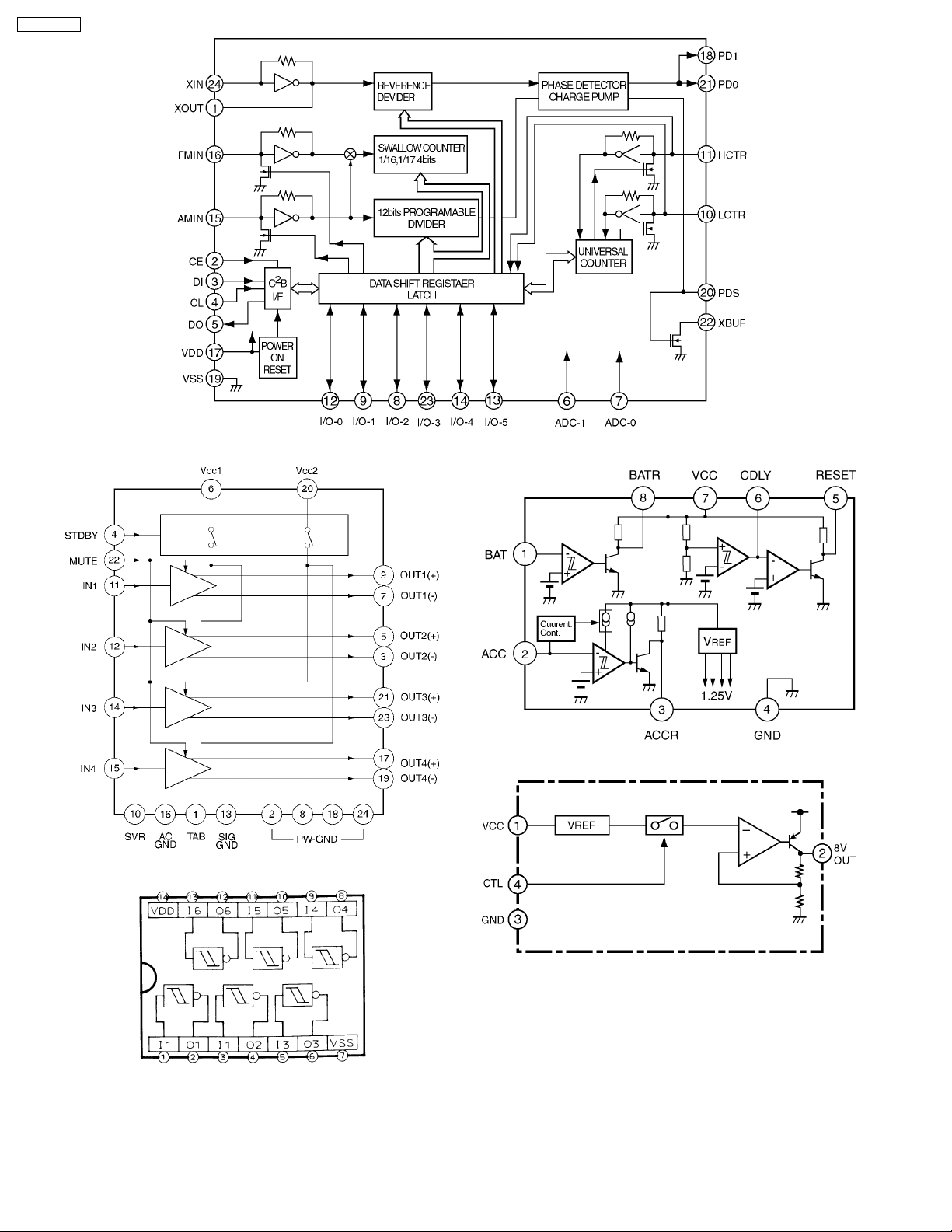
CQ-DPX172U
PA51 : C5BA00000092
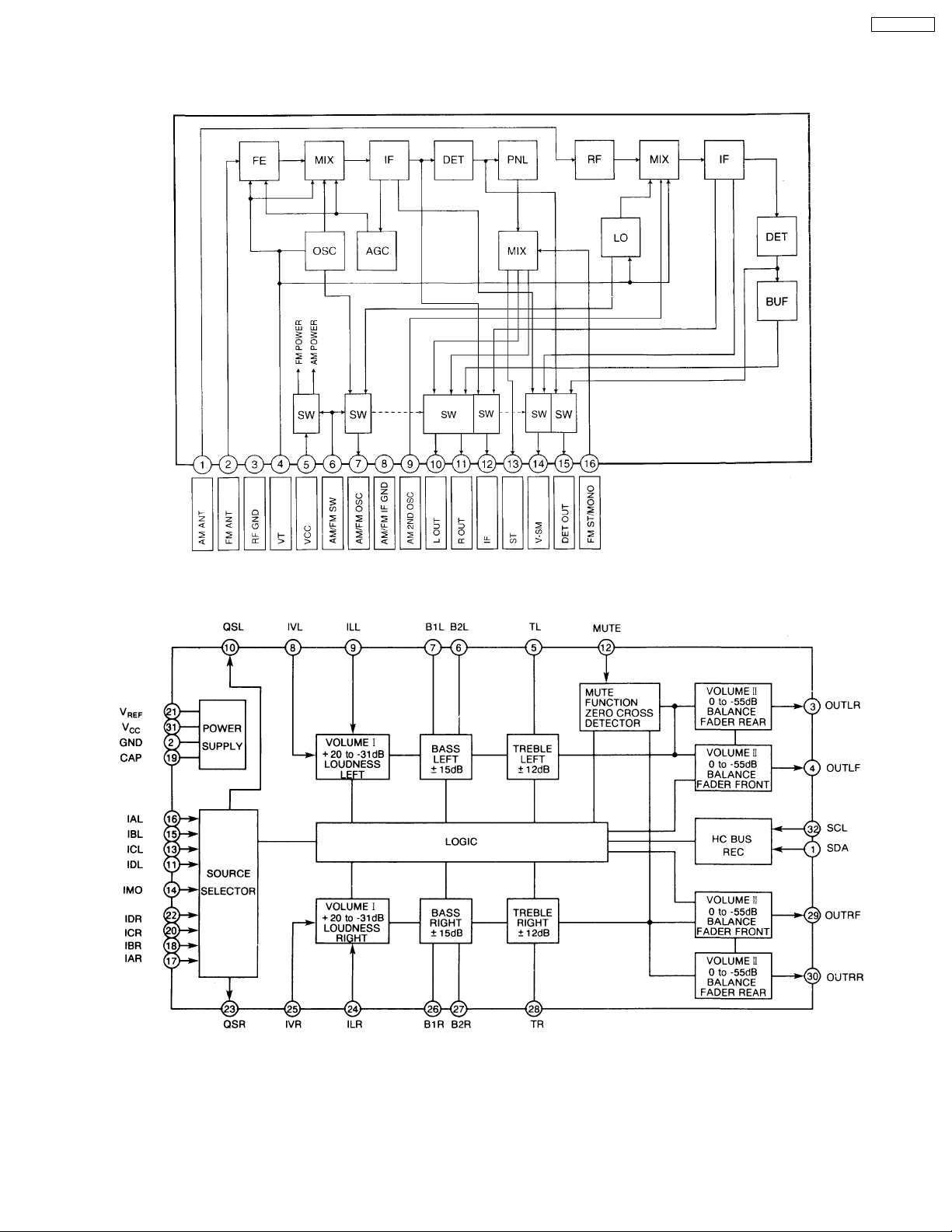
IC201 : YEAMEA6320TT
7
CQ-DPX172U
IC400 : C1BB00000541
IC270 : C1EA00000026
IC650 : YEAMC14584BE
IC601 : AN8065SE1
IC704 : C0DAZHF00003
8
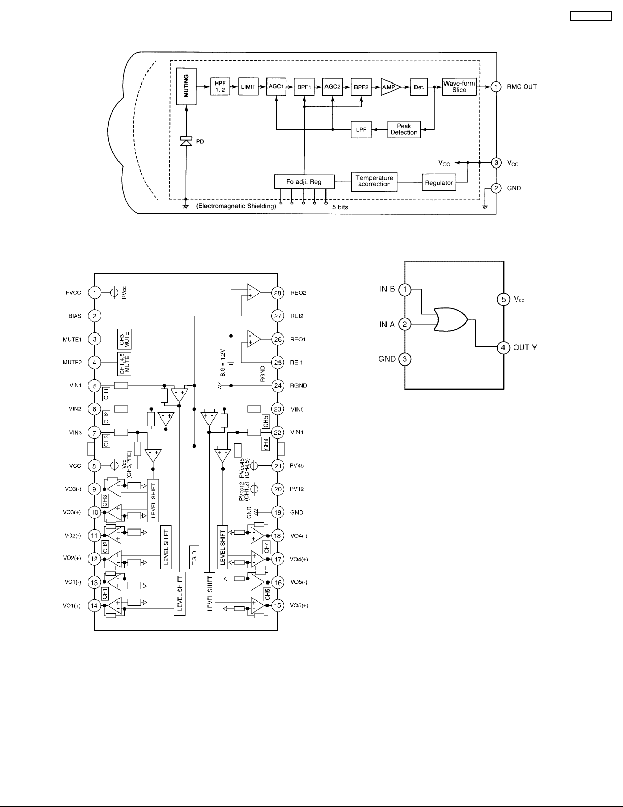
10.2. Display Block
10.3. CD Servo Block
CQ-DPX172U
IC902 : YEAMSBX8035F
IC901 : C0GBY0000012
IC441 : C0JBAE000087
IC541 : YEAMT7ST32UL
9
 Loading...