

Specifications*
ORDER NO. ACED051232C7
C4
AUTOMOTIVE AFTERMARKET
CQ-C7413U
CQ-C7113U
WMA MP3 CD Player/Receiver
General
Power Supply DC 12V (11V - 16V),
Test Voltage 14.4V
Negative Ground
Tone Controls (Bass/Treble) Bass: ±12dB at 60Hz
Treble: ±12dB at 16kHz
Equlizer Center Frequency 60, 160, 400, 1k, 3k, 6k, 16k Hz
(CQ-C7413U)
Equlizer Center Frequency Band 1 (60, 80, 100, 200 Hz)
Band 2 (500, 1k, 2k, 3k Hz)
Band 3 (10k, 12k, 15k, 18k Hz)
(CQ-C7113U)
Variable Range of Equalizer -12dB to 12dB (2dB step)
Current Consumption Less than 2.2A
(CD mode; 0.5W × 4-speaker)
Maximum Power Output 50W × 4(at 1kHz)
Speaker Impedance 4-8Ω
Pre-amp Output Voltage
<CQ-C7413U> 5V
(CD mode; 1kHz, 0dB)
<CQ-C7113U> 2V
(CD mode; 1kHz, 0dB)
Subwoofer Output Voltage
<CQ-C7413U> 5V
(CD mode; 1kHz, 0dB)
<CQ-C7113U> 2V
(CD mode; 1kHz, 0dB)
Pre-amp Output Impedance
<CQ-C7413U> 60Ω
<CQ-C7113U> 200Ω
Subwoofer Output Impedance
<CQ-C7413U> 60Ω
<CQ-C7113U> 200Ω
FM Stereo Radio
Frequency Range 87.9MHz - 107.9MHz
Usable Sensitivity 10.2dBf (0.9µV, 75Ω)
50dB Quieting Sensitivity 15.2dBf (1.6µV, 75Ω)
Frequency Response 30Hz-15kHz (±3dB)
Alternate Channel Selectivity 75dB
Stereo Separation 35dB (at 1kHz)
Image Response Ratio 75dB
IF Response Ratio 100dB
Signal to Noise Ratio 62dB
AM Radio
Frequency Range 530kHz - 1,710kHz
Usable Sensitivity 27dB/µV (S/N 20dB)
CD Player
Sampling Frequency 8 Times Oversampling
DA Converter 4 DAC System
Pick-up Type Astigma 3-Beam
Light Source Semiconductor Laser
Wave Length 790 nm
Frequency Response 20 Hz-20kHz (±1dB)
Signal to Noise Ratio 96dB
Total Harmonic Distortion 0.01% (1kHz)
Wow and Flutter Below Measurable Limits
Channel Separation 75dB
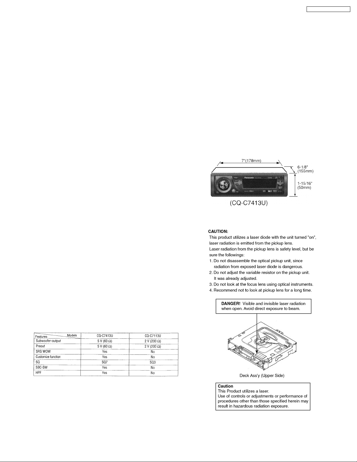
Dimensions (W×H×D)** 7”×1-15/16”×6-1/8”
(178×50×155mm)
Weight** 3 lbs. 8oz (1.6 kg)
© 2005 Matsushita Electric Industrial Co., Ltd. All
rights reserved. Unauthorized copying and
distribution is a violation of law.
CQ-C7413U / CQ-C7113U
* Specifications and the design are subject to possible modification
without notice due to improvements.
** Dimensions and Weight shown are approximate.
** Above specifications comply with EIA standards.
CONTENTS
Page Page
1 ABOUT LEAD FREE SOLDER (PbF)
2 FEATUERS
3 REPLACEING THE FUSE
4 MAINTENANCE
5 NOTES
6 DIMENSIONS
7 LASER PRODUCTS
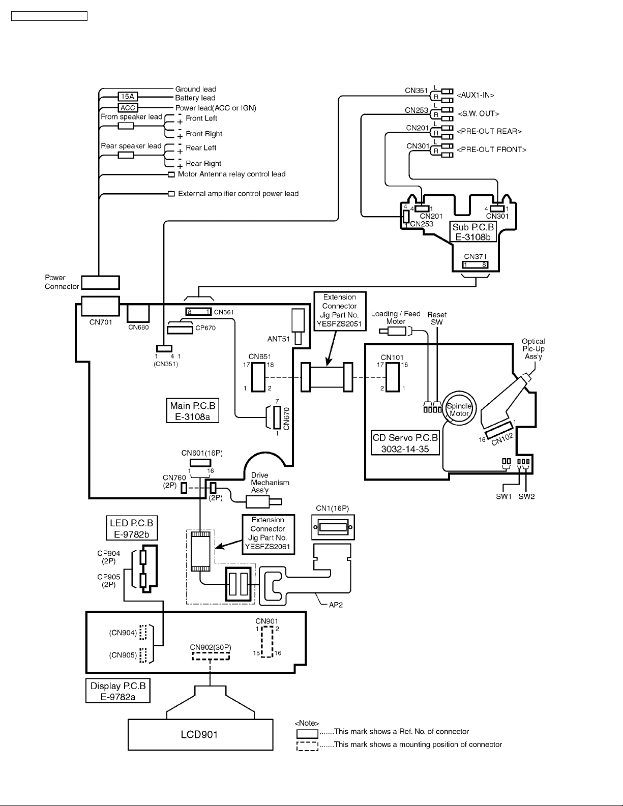
8 WIRING CONNECTION
9 DISASSEMBLY INSTRUCTIONS
10 TERMINALS DESCRIPTI ON
11 IC BLOCK DIAGRAM
3
12 PACKING PARTS LIST 16
13 REPLACEMENT PARTS LIST [CQ-C7413U ]
3
3
14 EXPLODED VIEW (Unit) [CQ-C7413U]
15 REPLACEMENT PARTS LIST [CQ-C7113U ]
3
3
16 EXPLODED VIEW (Unit) [CQ-C7113U]
3
17 CD PLAYER PARTS LIST
18 EXPLODED VIEW (CD PLAYER)
3
4
19 WIRING DIAGRAM
20 SCHEMATIC DIAGRAM-1
6
9
21 SCHEMATIC DIAGRAM-2
14
22 BLOCK DIAGRAM
17
23
24
30
31
34
35
42
43
49
2
CQ-C7413U / CQ-C7113U
1 ABOUT LEAD FREE
SOLDER (PbF)
Distinction of PbF PCB:
PCBs (manufactured) using lead free solder will have a PbF
stamp on the PCB.
Caution :
•
• Pb free solder has a higher melting point than standard
• •
solder; Typically the melting point is 50 - 70°F (30 40°C) higher. Please use a soldering iron with
temperature control and adjust it to 700 ± 20°F (370 ±
10°C). In case of using high temperature soldering iron,
please be careful not to heat too long.
•
• Pb free solder will tend to splash when heated too high
• •
(about 1100°F/600°C)
•
• This lead free solder will be used for the products after
• •
serial No. 1,000,001.
2 FEATUERS
•
• Hands Free Phone System. (The optional Bluetooth hands-
• •
free kit: CY-BT100U)
•
• Expansion Module (The optional Hub unit: CY-EM100U)
• •
•
• The optional adapter allows you to connect the optional
• •
Panasonic DVD changer unit (CX-DH801U).
•
• The optional adapter allows you to connect the optional
• •
Panasonic CD changer unit (CX-DP880).
•
• The optional adapter allows you to connect the optional
• •
®
iPod
series.
•
• XM Satellite Radio. (The optional XM receiver: XMD-1000)
• •
•
• Sirius Satellite Radio. (The optional Sirius Satellite receiver:
• •
SIR-PAN1)
•
• SQ (Sound Quality).
• •
•
• SQ7 (7-Band Sound Quality) [CQ-C7413U].
• •
•
• SQ3 (3-Band Sound Quality) [CQ-C7113U].
• •
•
• D.M(Direct Memory)
• •
•
• Customize the Display (Customize Function)
• •
•
• MP3/WMA Playback from CD-R/RW.
• •
•
• This manual is for 2 models CQ-C7413U and CQ-C7113U.
• •
The following table describes the differences between 2
models.
4 MAINTENANCE
Your products is designed and manufactured to ensure a
minimum of maintenance. Use a soft cloth for routine exterior
cleaning. Never use benzine, thinner or other solvent.
5 NOTES
[RADIO BLOCK]
Do not align the AM/FM package block. When the package
block is necessary, it will be supplied already aligned at the
factory.
[CD DECK BLOCK]
This model has no servo alignment points because
microcomputer controls the servo circuit
6 DIMENSIONS
7 LASER PRODUCTS
3 REPLACEING THE FUSE
Use fuses of the same specified rating 15 amps. Using different
substitutes or fuses with higher ratings, or connecting the unit
directly without a fuse, could cause fire or damage to the stereo
unit.
3
CQ-C7413U / CQ-C7113U
8 WIRING CONNECTION
8.1. CQ-C7413U
4
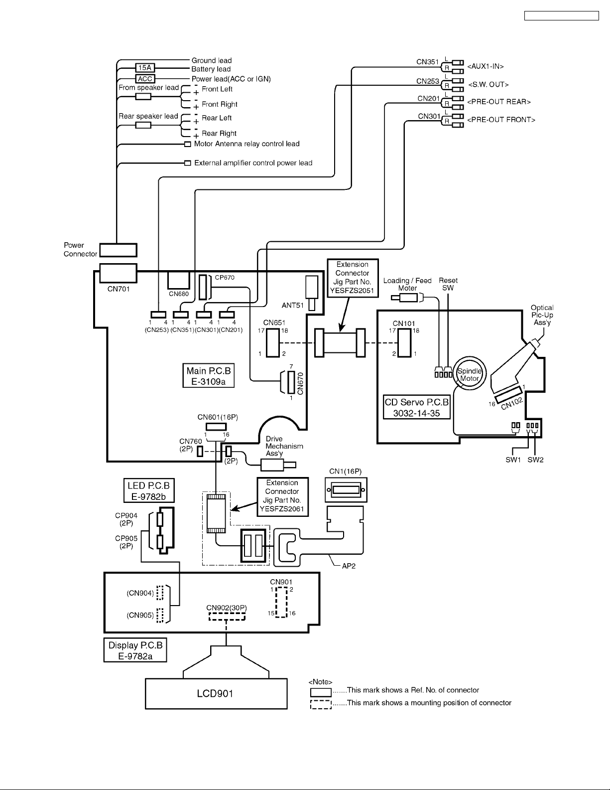
8.2. CQ-C7113U
CQ-C7413U / CQ-C7113U
5
CQ-C7413U / CQ-C7113U
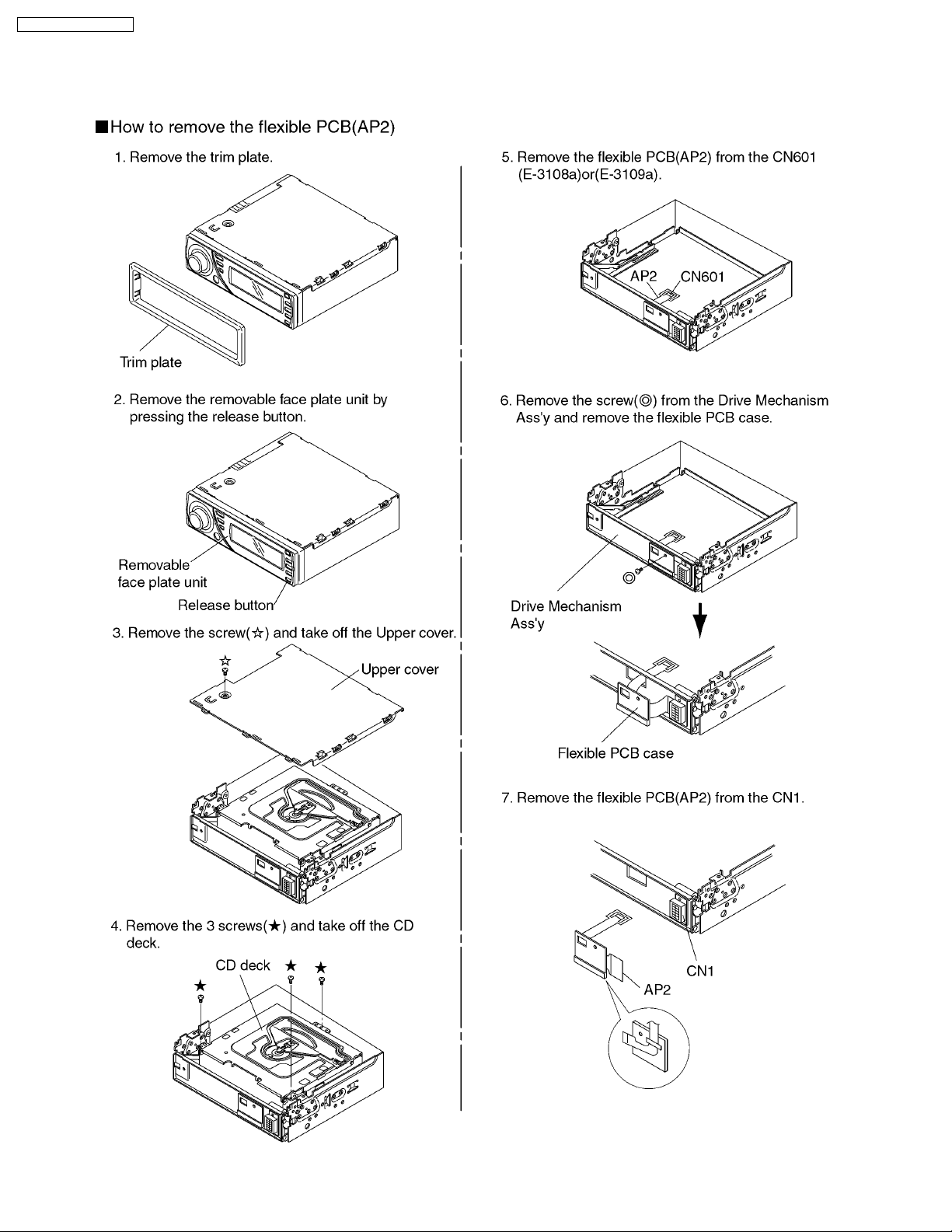
9 DISASSEMBLY INSTRUCTIONS
9.1. How to Remove the Flexible PCB(AP2)
6
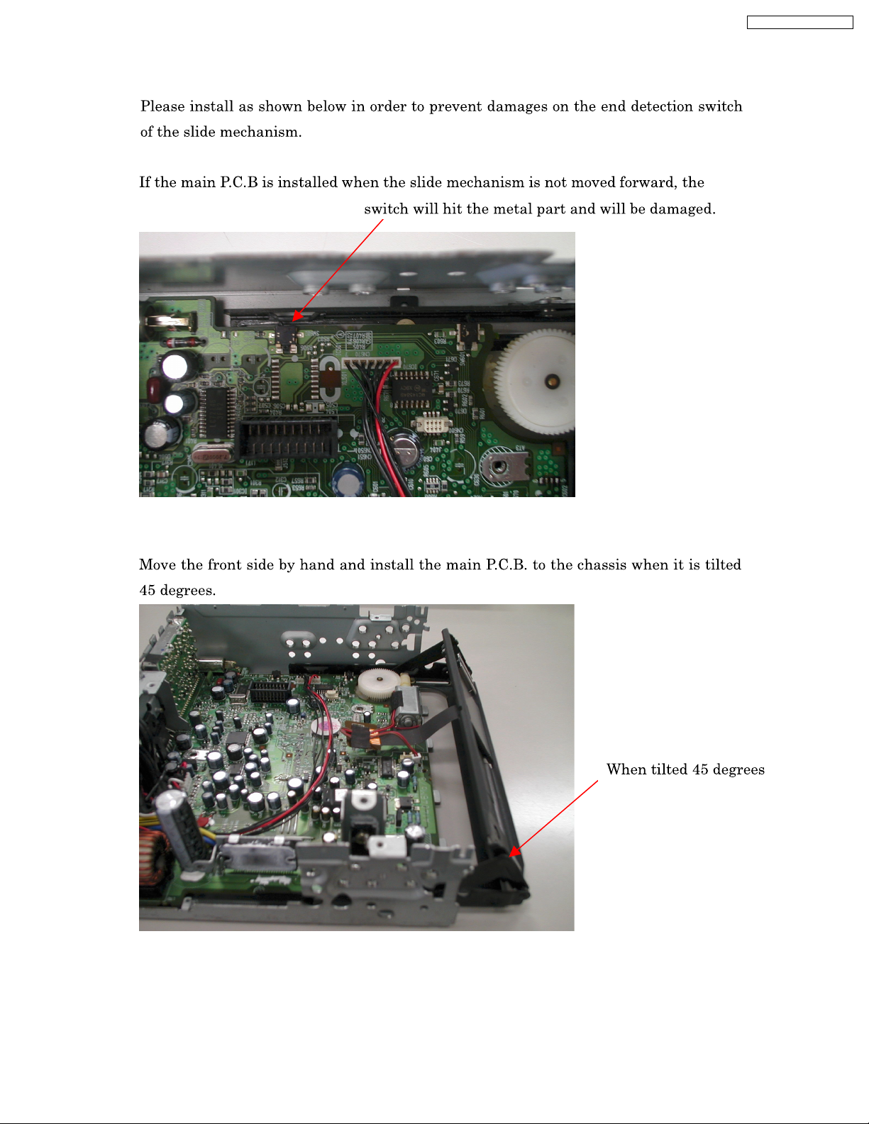
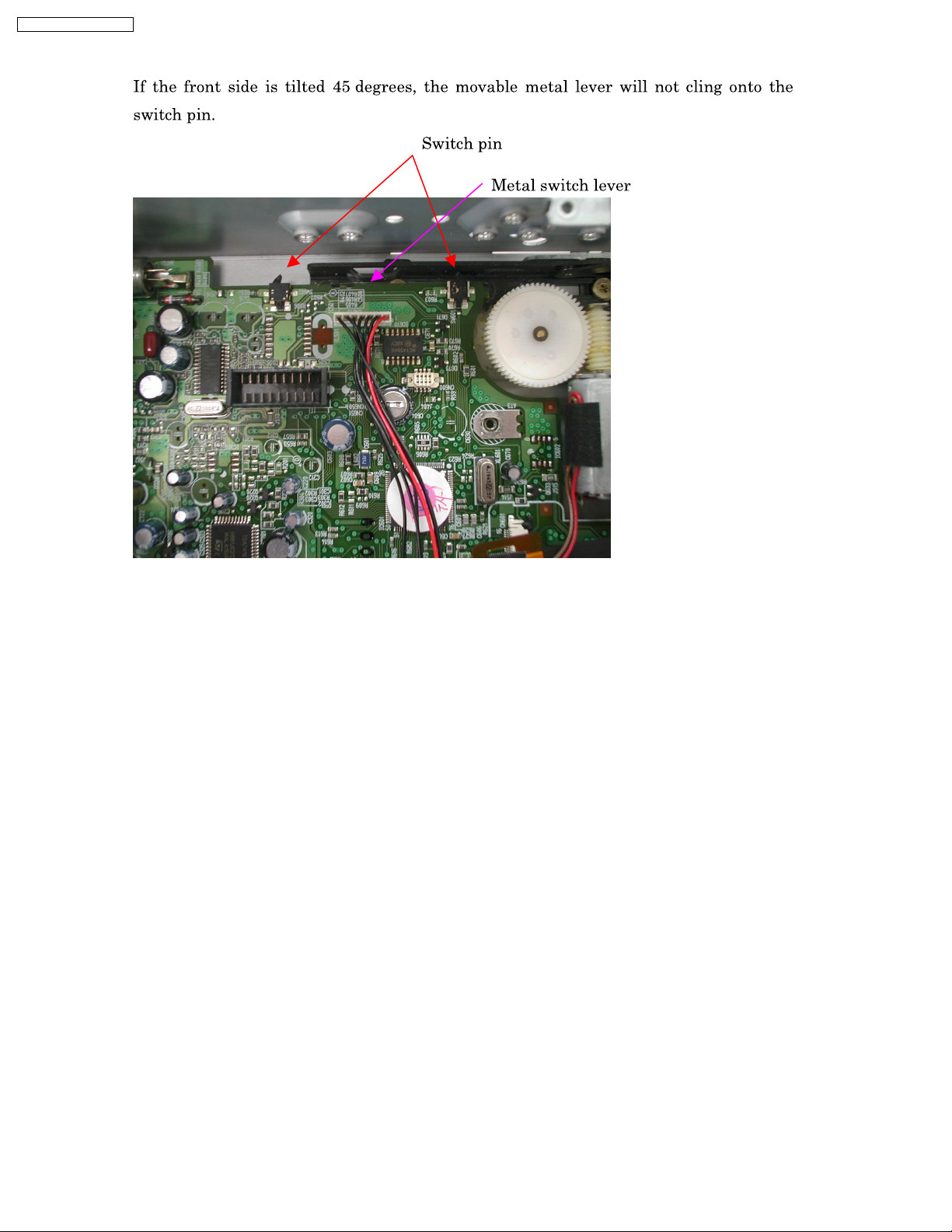
9.2. How to Install the Main P.C.B. of the Electric Display
CQ-C7413U / CQ-C7113U
7
CQ-C7413U / CQ-C7113U
8
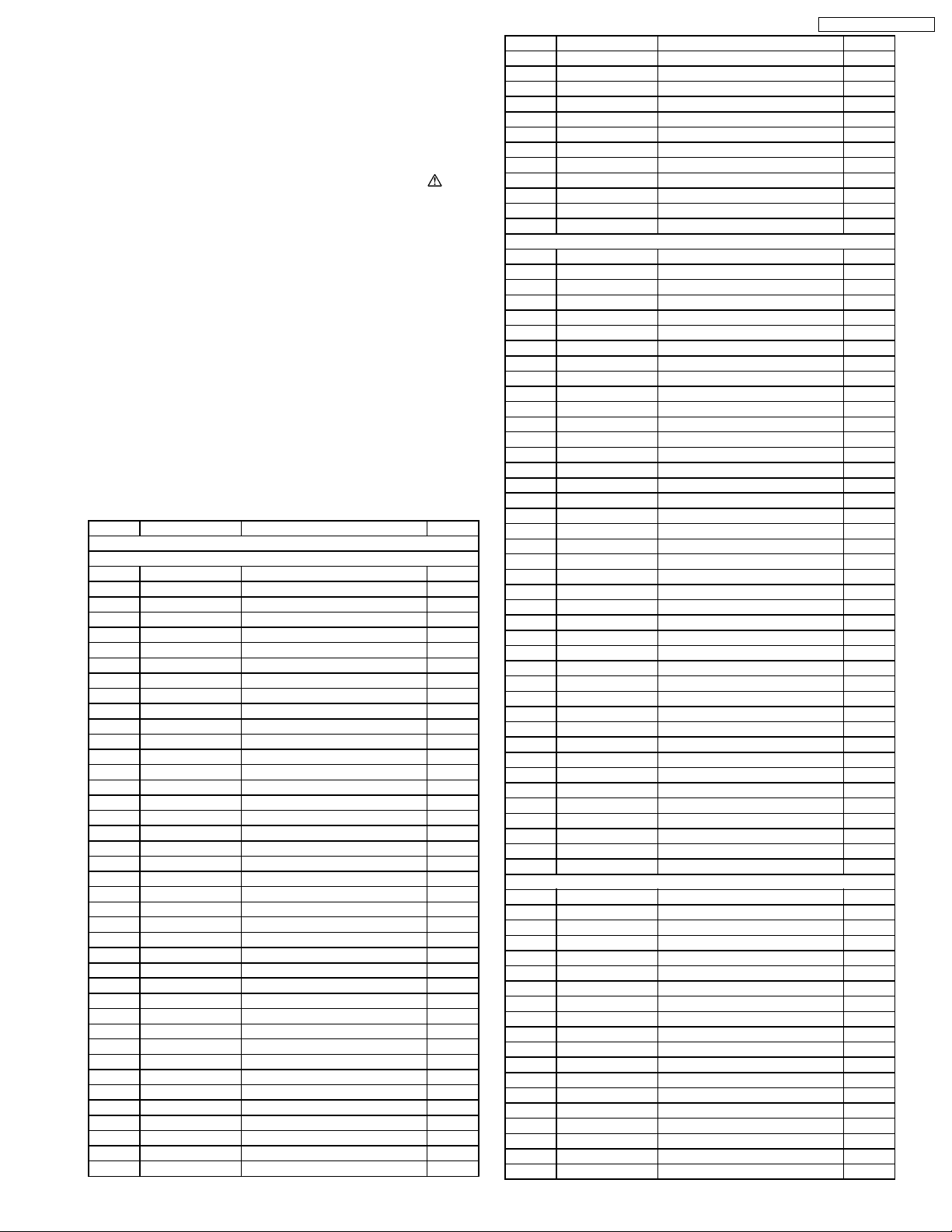
10 TERMINALS DESCRIPTION
CQ-C7413U / CQ-C7113U
10.1. Main Block [CQ-C7413U]
Pin
No.
1 PANEL OPEN Panel open detection I 0 5.2 5.2
2 PANEL CLOSE Panel close detection I 0 0 5.2
3 SUBM CNT 3.3V power control for
4 BATT Battery power check I 4.8 5 5
5 ACC Acc. power check I 4.8 5 5
6 SDA Serial data for
7 SCLK Serial clock for
8 CD MUTE Signal mute from CD
9 Vss GND - 0 0 0
10 ST FM stereo detection I 5.1 5.2 5.2
11 PLL DI (MO) Serial data to PLL O 0.6 0 0
12 PLL DO (MI) Serial data from PLL I 5.2 5.2 5.2
13 PLL CLK Serial clock for PLL O 4.9 4.9 4.9
14 PLL CE Chip enable for PLL O 0 0 0
15 CD RESET Reset for CD deck O 4.9 4.9 4.9
16 SUB SI Serial data to Display
17 CD IN Disc-in detection I 5 5 5
18 SUB SO Serial data from
19 CH DATA/ UPSOXM SO/UP SO Serial
20 CH CLK/ UP
21 Vdd +5V power supply - 4.9 4.9 4.9
22 XM SI (MO)/ UPSISerial data to Satellite
23 CD SI (MO) Serial data to CD deck O 0 0 0
24 CD SCLK Serial clock for CD
25 CONDENSOR Capacitor connection
26 CD SO (MI) Serial data from CD
27 CH STB Strobe from Changer I 0 0 0
28 CH REM OUT Remote control codes
29 DECK V CONT Power control for CD
30 REMO INT Interrupt for remote
31 CD FS Frame sync. for CD
32 Avdd +5V power supply - 5.1 5.1 5.1
33 AVREF +5V power supply - 5.1 5.1 5.1
34 AVGND GND - 0 0 0
35 AVSS GND - 0 0 0
36 SD FM/AM signal level
37 INIT A Model setting A by
38 INIT B Model setting B by
39 AIN Spectrum analyzer
40 Vss GND - 0 0 0
41 SYS ID1 Hub connection device
42 SYS ID2 Hub connection device
Port Part Name &
CLK
IC601 : C2CBKG000035
Description
Display
electronic volume
electronic volume
deck
CPU
Display CPU
data from Changer
Serial clock for
Changer or Flash
writer
or Flash writer
deck
for power
deck
to Changer
deck
control
deck
meter
voltage level
voltage level
data
detection ID 1
detection ID 2
I/O FM AM CD
O 5 - -
I/O 4.9 4.9 4.9
O 4.9 4.9 4.9
I 5 5 5
O 0.6 0.6 0.8
I 4.4 4.4 4.4
I 1.6 1.6 1.6
I 4.9 4.9 4.9
O 0 0 0
I/O 0 0.4 0
- 3.3 3.3 3.3
I 0 0 0
O 4.9 4.9 0.4
O 4.9 4.9 4.9
I 3.7 3.7 3.7
O - - -
I 0.2 0 0.3
I 0 0 0
I 0 0 0
I 0 0 0
I 0 0 0
I 5.2 5.2 5.2
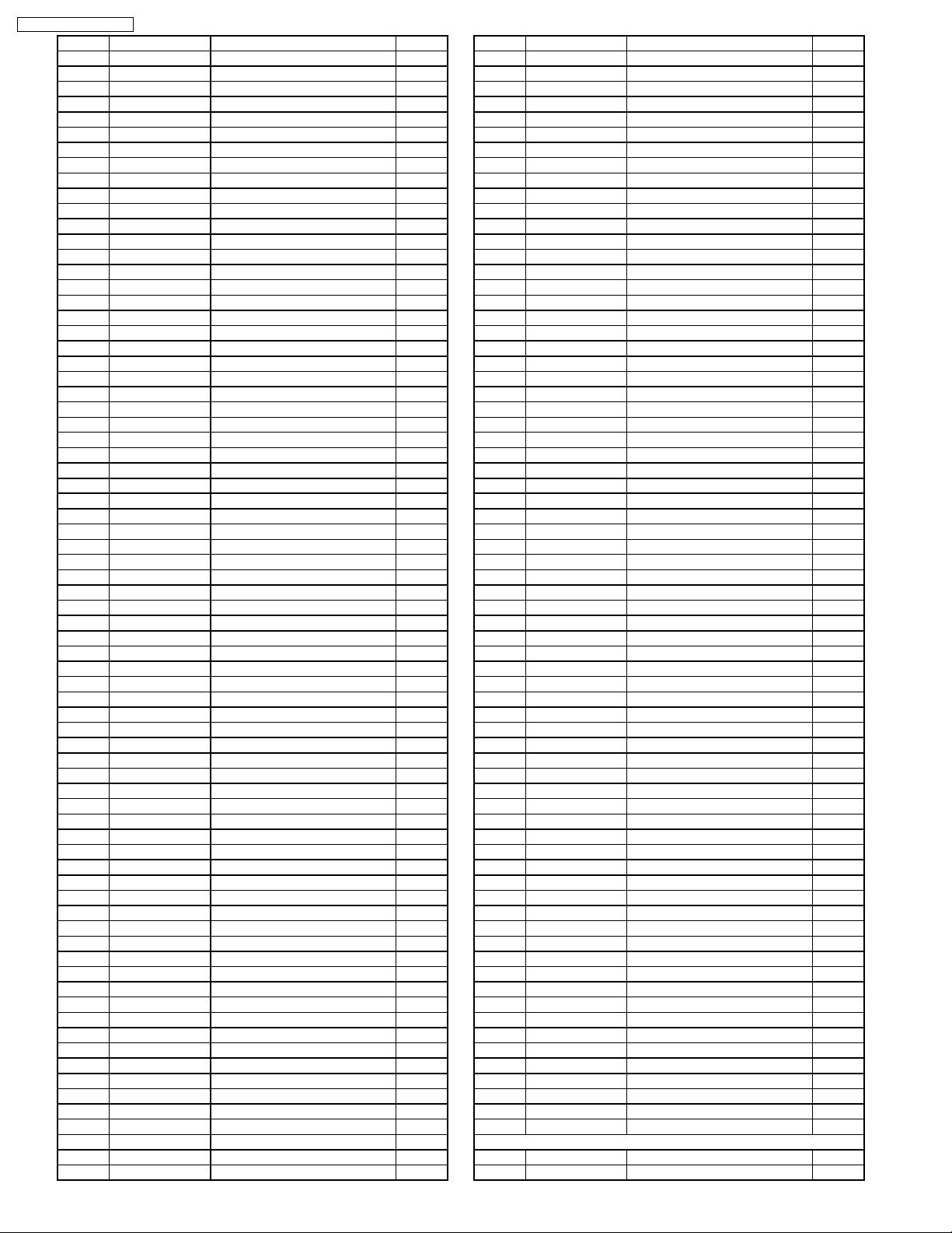
Pin
No.
43 HUB EVENT Bluetooth incoming
44 HUB CNT Request of hub
45 CD SW1 Disc detection switch 1 I 0 0 0
46 CD SW2 Disc detection switch 2 I 0 0 0
47 MOD0 Operating mode
48 MOD1 Operating mode
49 MOD2 Operating mode
50 H STANDBY Standby control from
51 DCDC CONT Not connected - - - 52 FP MOTOR1 Open/Close of Front
53 FP MOTOR2 Open/Close of Front
54 V CONT1 Reference voltage
55 REMO 1 Remote control data I 5 5 5
56 SA CLK Spectrum analyzer
57 EXT MUTE Pulled up to H I 5.3 5.2 5.2
58 AMP CONT Power control for
59 BZ OUT Buzzer signal O 0 0 0
60 OEL VCONT Not connected - - - 61 WOW MODE1 SRS WOW mode 1 O 0 0 0
62 WOW MODE2 SRS WOW mode 2 O 0 0 0
63 WOW MODE3 SRS WOW mode 3 O 0 0 0
64 DIM1 Not connected - - - 65 DIM2 Not connected - - - 66 MAIN CNT2 Power control for Hub O 5 5 5
67 SRC KEY SOURCE key
68 PANEL IN Panel attachment
69 RDS CLK Not connected - - - 70 NC Not connected - - - 71 RDS DATA Not connected - - - 72 MAIN CONT Main power control O 4.9 4.9 4.9
73 INV CONT Dimmer power control O 5 5 5
74 AF MUTE Audio mute O 5 5 5
75 RESET Reset I 5 5 5
76 FOCUS ELV Focus elevation for
77 X1A Oscillator clock O 2.1 2.1 2.1
78 X0A Oscillator clock I 1.6 1.6 1.6
79 Vss GND - 0 0 0
80 X1 Crystal oscillator clock I 2 2 2
81 X2 Crystal oscillator clock O 2.5 2.5 2.5
82 Vdd +5V power supply - 5 5 5
83 P00 Pulled down to L - 0 0 0
84 P01 Pulled up to H - 5.1 5 5.1
85 OFFSET DET Audio clipping level
86 STBY Standby for Power
87 MUTE Mute for Power amp. O 0 0 0
88 ILL SENS Pulled up to H - 5 5 5
89 NC Not connected - - - -
Port Part Name &
Description
detection
connection check
control 0 from Flash
writer
control 1: pulled up to
H
control 2 from Flash
writer
external
panel 1
panel 2
control for motor driver
clock
external Amplifier
detection
detection
SRS WOW
detection from Power
amp.
amp.
I/O FM AM CD
I 5.2 5.2 5.2
O 0 0 0
I 5.1 5.1 5.1
- 5.1 5.1 5.1
I 0 0 0
I 5 5 5
O 4.9 5 4.9
O 4.9 5 4.9
O 0 0 5
O 5 5 4.9
O 4.9 5 4.9
I 5 4.9 5
I - - -
O - - -
I 0 0 0
O 5 5 5
9
CQ-C7413U / CQ-C7113U
Pin
No.
90 PE DO(MI) - - - - 91 NC Not connected - - - 92 NC Not connected - - - 93 SUB RESET Reset for display CPU O 4.9 5 4.9
94 DISPM CONT 5V power control for
95 NC Not connected - - - 96 NC Not connected - - - 97 NC Not connected - - - 98 S LED Security LED drive O 0 0 5
99 ANT CONT Power control for
100 EP CS Not connected - - - -
Port Part Name &
Description
Display
antenna motor
I/O FM AM CD
O 0 0 0
O 5.2 5.2 5.2
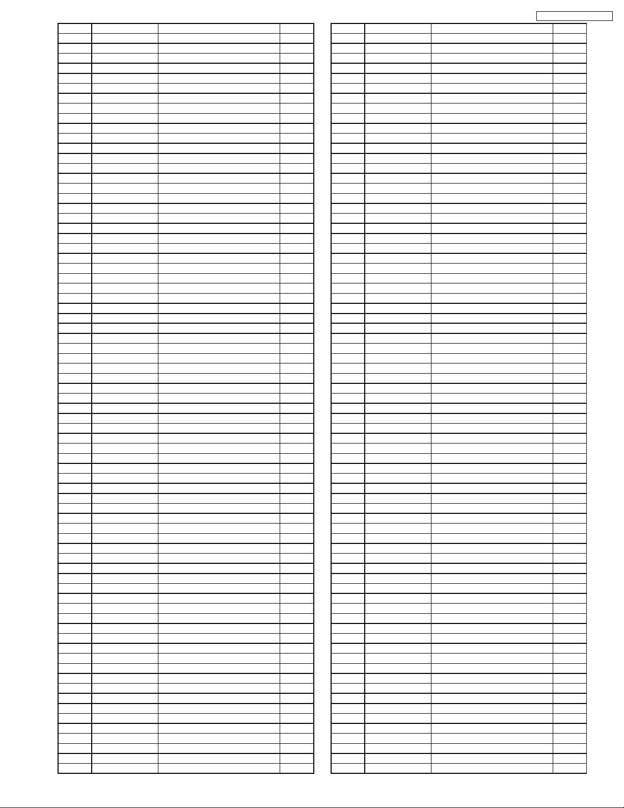
10.2. Main Block [CQ-C7113U]
Pin
No.
1 PANEL OPEN Panel open detection I 0 5.2 5.2
2 PANEL CLOSE Panel close detection I 0 0 5.2
3 SUBM CNT 3.3V power control for
4 BATT Battery power check I 4.8 5 5
5 ACC Acc. power check I 4.8 5 5
6 SDA Serial data for
7 SCLK Serial clock for
8 CD MUTE Signal mute from CD
9 Vss GND - 0 0 0
10 ST FM stereo detection I 5.1 5.2 5.2
11 PLL DI (MO) Serial data to PLL O 0.6 0 0
12 PLL DO (MI) Serial data from PLL I 5.2 5.2 5.2
13 PLL CLK Serial clock for PLL O 4.9 4.9 4.9
14 PLL CE Chip enable for PLL O 0 0 0
15 CD RESET Reset for CD deck O 4.9 4.9 4.9
16 SUB SI Serial data to Display
17 CD IN Disc-in detection I 5 5 5
18 SUB SO Serial data from
19 CH DATA/ UPSOXM SO/UP SO Serial
20 CH CLK/ UP
21 Vdd +5V power supply - 4.9 4.9 4.9
22 XM SI (MO)/ UPSISerial data to Satellite
23 CD SI (MO) Serial data to CD deck O 0 0 0
24 CD SCLK Serial clock for CD
25 CONDENSOR Capacitor connection
26 CD SO (MI) Serial data from CD
27 CH STB Strobe from Changer I 0 0 0
28 CH REM OUT Remote control codes
29 DECK V CONT Power control for CD
30 NC Not connected - - - 31 CD FS Frame sync. for CD
32 Avdd +5V power supply - 5.1 5.1 5.1
33 AVREF +5V power supply - 5.1 5.1 5.1
34 AVGND GND - 0 0 0
35 AVSS GND - 0 0 0
36 SD FM/AM signal level
37 INIT A Model setting A by
38 INIT B Model setting B by
39 AIN Spectrum analyzer
40 Vss GND - 0 0 0
41 SYS ID1 Hub connection device
42 SYS ID2 Hub connection device
43 HUB EVENT Bluetooth incoming
Port Part Name &
CLK
IC601 : C2CBKG000035
Description
Display
electronic volume
electronic volume
deck
CPU
Display CPU
data from Changer
Serial clock for
Changer or Flash
writer
or Flash writer
deck
for power
deck
to Changer
deck
deck
meter
voltage level
voltage level
data
detection ID 1
detection ID 2
detection
I/O FM AM CD
O 5 - -
I/O 4.9 4.9 4.9
O 4.9 4.9 4.9
I 5 5 5
O 0.6 0.6 0.8
I 4.4 4.4 4.4
I 1.6 1.6 1.6
I 4.9 4.9 4.9
O 0 0 0
I/O 0 0.4 0
- 3.3 3.3 3.3
I 0 0 0
O 4.9 4.9 0.4
O 4.9 4.9 4.9
O - - -
I 0.2 0 0.3
I 0 0 0
I 0 0 0
I 0 0 0
I 0 0 0
I 5.2 5.2 5.2
I 5.2 5.2 5.2
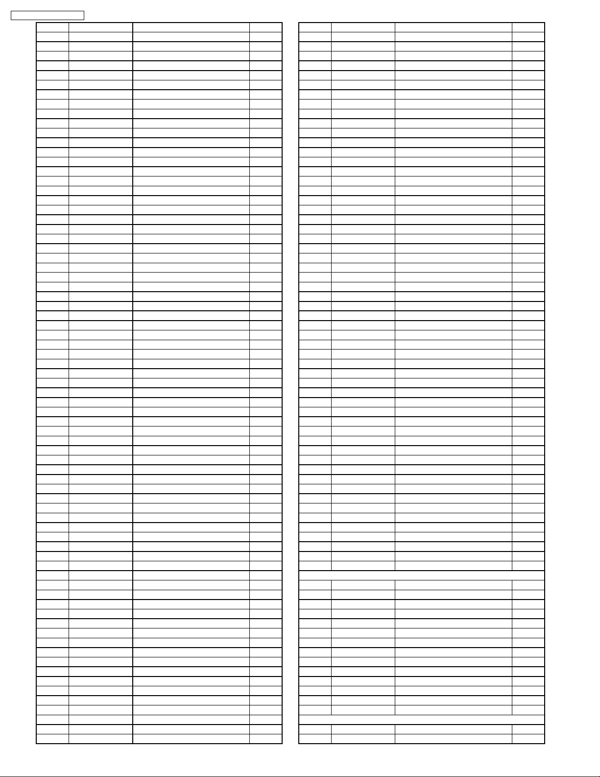
10
Pin
No.
44 HUB CNT Request of hub
Port Part Name &
Description
I/O FM AM CD
O 0 0 0
connection check
45 CD SW1 Disc detection switch 1 I 0 0 0
46 CD SW2 Disc detection switch 2 I 0 0 0
47 MOD0 Operating mode
I 5.1 5.1 5.1
control 0 from Flash
writer
48 MOD1 Operating mode
- 5.1 5.1 5.1
control 1: pulled up to
H
49 MOD2 Operating mode
I 0 0 0
control 2 from Flash
writer
50 H STANDBY Standby control from
I 5 5 5
external
51 DCDC CONT Not connected - - - 52 FP MOTOR1 Open/Close of Front
O 4.9 5 4.9
panel 1
53 FP MOTOR2 Open/Close of Front
O 4.9 5 4.9
panel 2
54 V CONT1 Reference voltage
O 0 0 5
control for motor driver
55 REMO 1 Remote control data I 5 5 5
56 SA CLK Spectrum analyzer
O 5 5 4.9
clock
57 EXT MUTE Pulled up to H I 5.3 5.2 5.2
58 AMP CONT Power control for
O 4.9 5 4.9
external Amplifier
59 BZ OUT Buzzer signal O 0 0 0
60 NC Not connected - - - 61 WOW MODE1 Not connected - - - 62 WOW MODE2 Not connected - - - 63 WOW MODE3 Not connected - - - 64 DIM1 Not connected - - - 65 DIM2 Not connected - - - 66 MAIN CNT2 Power control for Hub O 5 5 5
67 SRC KEY SOURCE key
I 5 4.9 5
detection
68 PANEL IN Panel attachment
I - - detection
69 NC Not connected - - - 70 NC Not connected - - - 71 NC Not connected - - - 72 MAIN CONT Main power control O 4.9 4.9 4.9
73 INV CONT Dimmer power control O 5 5 5
74 AF MUTE Audio mute O 5 5 5
75 RESET Reset I 5 5 5
76 FOCUS ELV Not connected - - - 77 X1A Oscillator clock O 2.1 2.1 2.1
78 X0A Oscillator clock I 1.6 1.6 1.6
79 Vss GND - 0 0 0
80 X1 Crystal oscillator clock I 2 2 2
81 X2 Crystal oscillator clock O 2.5 2.5 2.5
82 Vdd +5V power supply - 5 5 5
83 P00 Pulled down to L - 0 0 0
84 P01 Pulled up to H - 5.1 5 5.1
85 OFFSET DET Audio clipping level
I 0 0 0
detection from Power
amp.
86 STBY Standby for Power
O 5 5 5
amp.
87 MUTE Mute for Power amp. O 0 0 0
88 ILL SENS Pulled up to H - 5 5 5
89 NC Not connected - - - 90 NC Not connected - - - 91 NC Not connected - - - 92 NC Not connected - - - 93 SUB RESET Reset for display CPU O 4.9 5 4.9
CQ-C7413U / CQ-C7113U
Pin
No.
94 DISPM CONT 5V power control for
Port Part Name &
Description
I/O FM AM CD
O 0 0 0
Display
95 EJE IU Not connected - - - 96 NC Not connected - - - 97 NC Not connected - - - 98 S LED Security LED drive O 0 0 5
99 ANT CONT Power control for
O 5.2 5.2 5.2
antenna motor
100 EP CS Not connected - - - -
11
CQ-C7413U / CQ-C7113U
10.3. Display Block
IC900 : C2CBJH000133 [CQ-C7413U]
Pin
No.
1 A18 A18 in Address bus O 1.5
2 A19 A19 in Address bus O 1.7
3 A20 A20 in Address bus O 1.3
4 NC Not connected - 5 LED G - - 6 LED B - - 7 A0 A0 in address bus for LCD O 1.3
8 A1 A1 in Address bus O 0.3
9 VSS GND - 10 A2 A2 in Address bus O 0.4
11 A3 A3 in Address bus O 0.4
12 A4 A4 in Address bus O 0.4
13 A5 A5 in Address bus O 1.3
14 A6 A6 in Address bus O 0.4
15 A7 A7 in Address bus O 0
16 A8 A8 in Address bus O 1.3
17 A9 A9 in Address bus O 0
18 A10 A10 in Address bus O 0
19 A11 A11 in Address bus O 1.5
20 A12 A12 in Address bus O 1.7
21 VCC +3.3V Power supply - 3.5
22 A13 A13 in Address bus O 1.4
23 A14 A14 in Address bus O 1.5
24 A15 A15 in Address bus O 1.7
25 SIN0 Serial data from Main CPU or Flash
26 SOT0 Serial data to Main CPU or Flash
27 SCK0 Serial clock for Flash writer I 3.5
28 NC Not connected - 29 FRASH
30 KS1 Key scan 1 O 0
31 NC Not connected - 32 NC Not connected - 33 AVCC +3.3V Power supply - 3.5
34 AVRH +3.3V Power supply - 3.5
35 AVSS/
36 TH
37 KS2 Key scan 2 O 0
38 KS3 Key scan 3 O 0
39 NC Not connected - 40 VSS GND - 41 KI5 Key-in return 5 I 0
42 KI4 Key-in return 4 I 0
43 KI3 Key-in return 3 I 0
44 KI2 Key-in return 2 I 0
45 NC Pulled down to L - 0
46 NC Pulled up to H - 3.5
47 MD0 Operating mode control 0 from Flash
48 MD1 Operating mode control 1: pulled up
49 MD2 Operating mode control 2 from Flash
50 NC Not connected - 51 ROTA
52 ROTA
53 NC Not connected - -
IC900 : C2CBJH000134 [CQ-C7113U]
Port Part Name & Description I/O (V)
writer
writer
RESET
AVRL
DETEC
T
RY 1
RY 2
Reset for Flash memory O 3.5
GND - -
Pulled up to H - 1.3
writer
to H
writer
Volume-up detection from Rotary
encoder
Volume-down detection from Rotary
encoder
I 0.5
O 1.8
I 3.5
- 3.5
I 0
I 2.5
I 2.5
Pin
Port Part Name & Description I/O (V)
No.
54 NC Not connected - 55 NC Not connected - 56 NC Not connected - 57 NC Not connected - 58 FLASHCEChip enable for Flash memory O 3.4
59 LCDCSLCD chip select O 3.4
60 LED R
61 NC Not connected - 62 NC Not connected - 63 NC Not connected - 64 VLCD
CONT
65 NC Not connected - 66 NC Not connected - 67 NC Not connected - 68 NC Not connected - 69 OE/RD Output enable for Flash memory or
70 LCDWRWrite strobe for LCD O 3.4
71 FLASHWEWrite enable for Flash memory O 3.4
72 NC Not connected - 73 LCD
RESET
74 FLASH
RY/BY
75 RST Reset I 3.5
76 NC Not connected - 77 NC Not connected - 78 X0A GND - 79 VSS GND - 80 X0 System clock (12.5MHz) I 1.3
81 X1 System clock (12.5MHz) O 1.5
82 VCC +3.3V Power supply - 3.5
83 D0 D0 in Data bus I/O 0.9
84 D1 D0 in Data bus I/O 0.9
85 D2 D0 in Data bus I/O 1.1
86 D3 D0 in Data bus I/O 0.9
87 D4 D0 in Data bus I/O 1.0
88 D5 D0 in Data bus I/O 1.1
89 D6 D0 in Data bus I/O 1.1
90 D7 D0 in Data bus I/O 0.9
91 D8 D0 in Data bus I/O 0.9
92 D9 D0 in Data bus I/O 0.9
93 D10 D0 in Data bus I/O 0.9
94 D11 D0 in Data bus I/O 0.5
95 D12 D0 in Data bus I/O 0.9
96 D13 D0 in Data bus I/O 0.7
97 D14 D0 in Data bus I/O 0.7
98 D15 D0 in Data bus I/O 0.7
99 A16 A16 in Address bus O 3.0
100 A17 A17 in Address bus O 1.7
Power control for LCD O 3.4
O 3.4
Read strobe for LCD
Reset for LCD O 3.4
Ready/Busy from Flash memory I 3.4
12
10.4. CD Servo Block
IC101 : YESAM337
Pin No. Port Descriptions I/O (V)
1 AVSS GND - 0
2 LD-MT Loading Motor drive IC control 1 O 3.2
3 CNT Loading Motor drive IC control 2 O 3.2
4 - - - 5 LD-EJ Loading Motor drive IC control
(Eject)
6 AMUTE Mute signal output O 0
7 - - - 8 SBSY DSP IC SBSY O 0
9 - - - -
10 - - - 11 TXD0 Serial data output O 0
12 RXD0 Serial data input I 0
13 CLK0 Clock input I 2.9
14 - - - 15 - - - 16 - - - 17 AMD - - 3.2
18 DVCC Power supply (3.3V) - 3.2
19 X2 Crystal oscillator - 1.3
20 DVSS GND - 0
21 X1 Crystal oscillator - 1.3
22 AMI - - 3.2
23 RESET Reset I 3
24 - - - 25 - - - 26 NMI - - 3.2
27 - - - 28 STBY DSP IC STBY O 0
29 RST DSP IC RST O 3.2
30 CCE DSP IC CCE O 2.6
31 BUCK DSP IC CK O 2.8
32 BUS3 DSP IC BUS3 O 2.8
33 BUS2 DSP IC BUS2 O 2.8
34 BUS1 DSP IC BUS1 O 2.8
35 BUS0 DSP IC BUS0 O 2.9
36 RESETSWMechanics deck REST SW input I 3.2
O 0
CQ-C7413U / CQ-C7113U
37 SW1 Mechanics deck SW1 input I 0
38 SW2 Mechanics deck SW2 input I 0
39 CONT
(P13)
40 - - - 41 - - - 42 - - - 43 CONT
(P17)
44 PIO0 DSP IC PIO0 O 0
45 ZDET LOAD detect I 0
46-48 - - - -
49 - - - 3.2
50-58 - - - -
59 CDFS Serial frame sink signal input
60 P50/AN0 Reference voltage I 0.3
61 P51/AN0 Loading motor detect I 2.1
62 P52/AN2 - - 0
63 P53/AN3 - - 0
64 AVCC Power supply (3.3V) - 3.2
DSP IC power control 1 O 3.2
DSP IC power control 2 O 3.2
I 2.3
(CD ON)
13
CQ-C7413U / CQ-C7113U
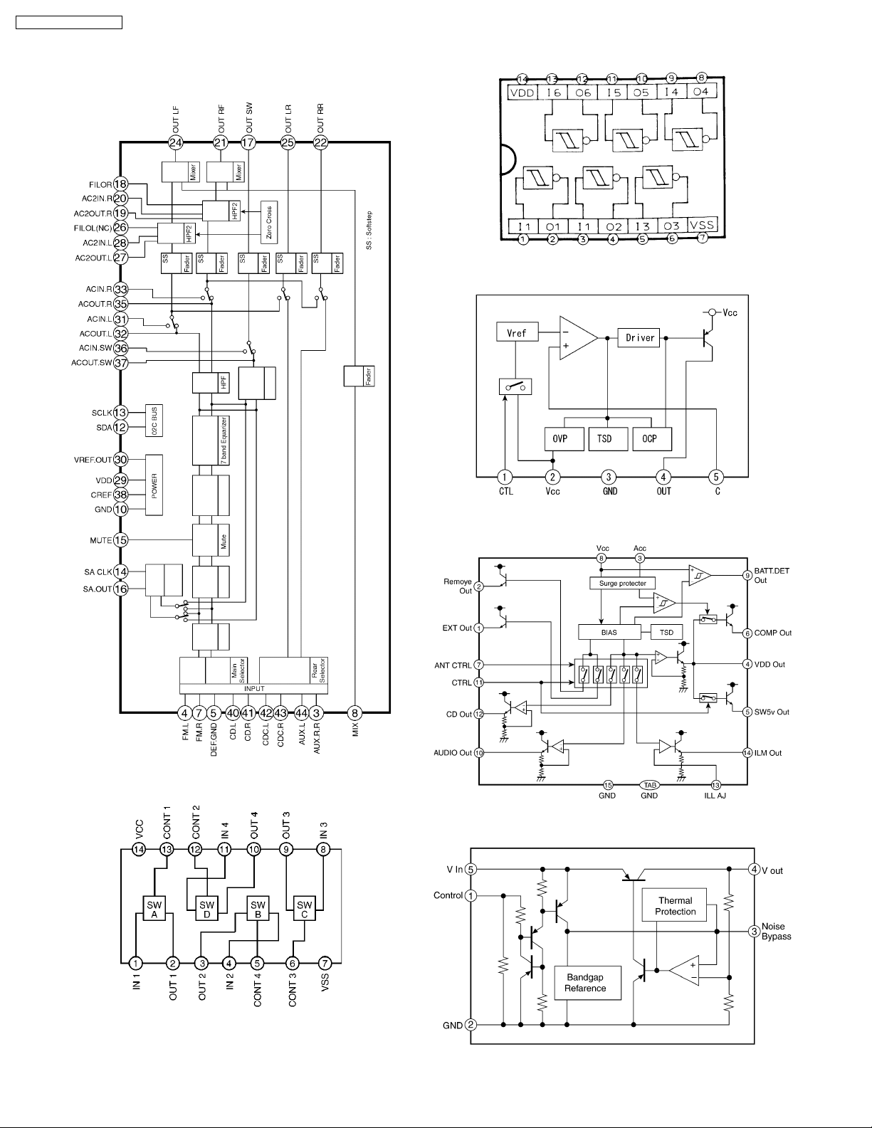
11 IC BLOCK DIAGRAM
11.1. Main Block
IC670 : YEAMC14584BE
IC201 : C1BB00000796
IC730 : C0DAEKG00002
IC701 : C0DAZHF00004
IC231 : C0JBZS000003 [CQ-C7413U]
IC755 : C0DBZGD00040
14
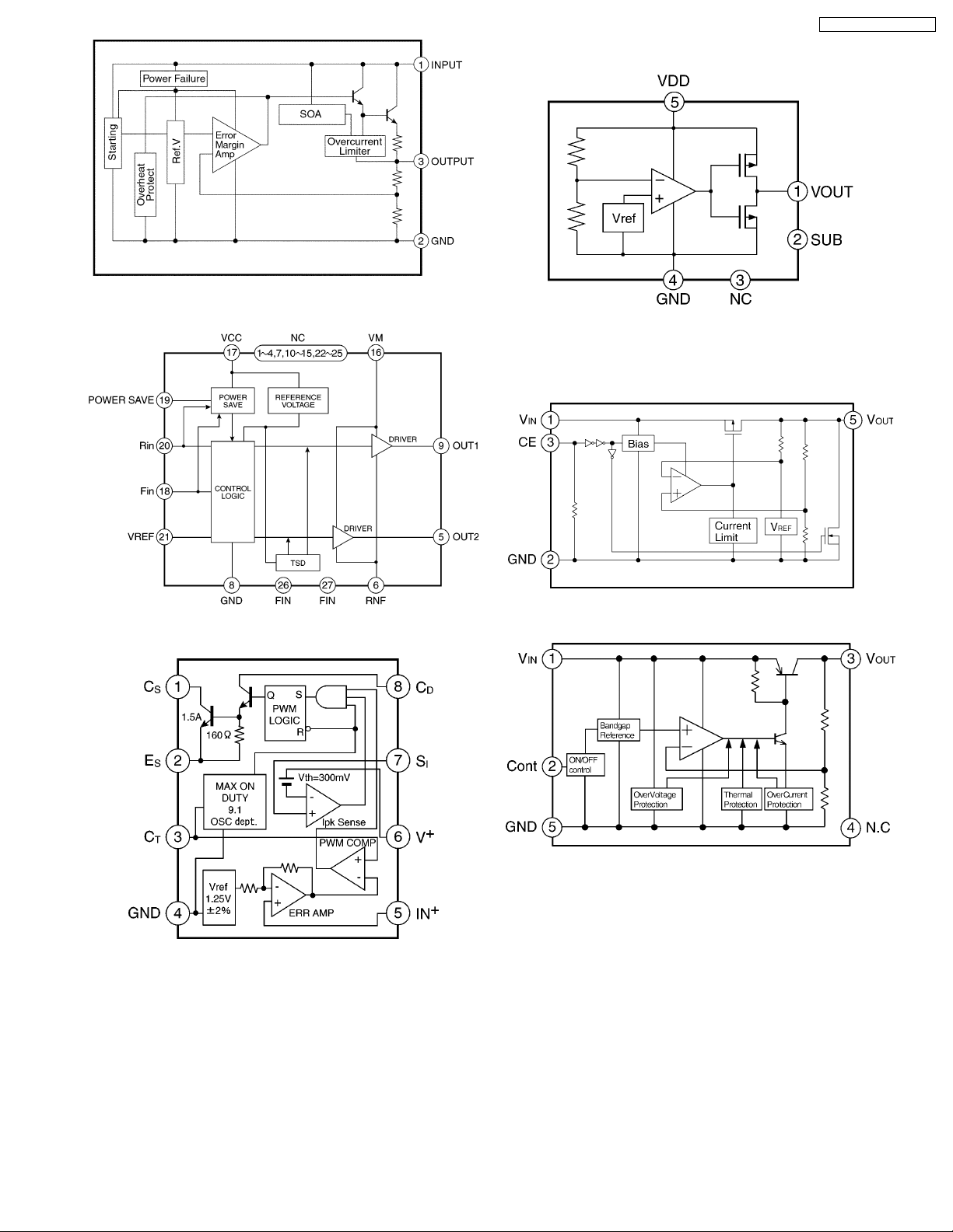
IC752 : C0CAABG00012
CQ-C7413U / CQ-C7113U
11.2. Display Block
IC902 : C0EBF0000374
11.3. CD Servo Block
IC760 : C0GBG0000032
IC770 : C0DBAHG00020 [CQ-C7413U]
IC401, IC403 : YESAM341
IC402 : YESAM342
15
CQ-C7413U / CQ-C7113U
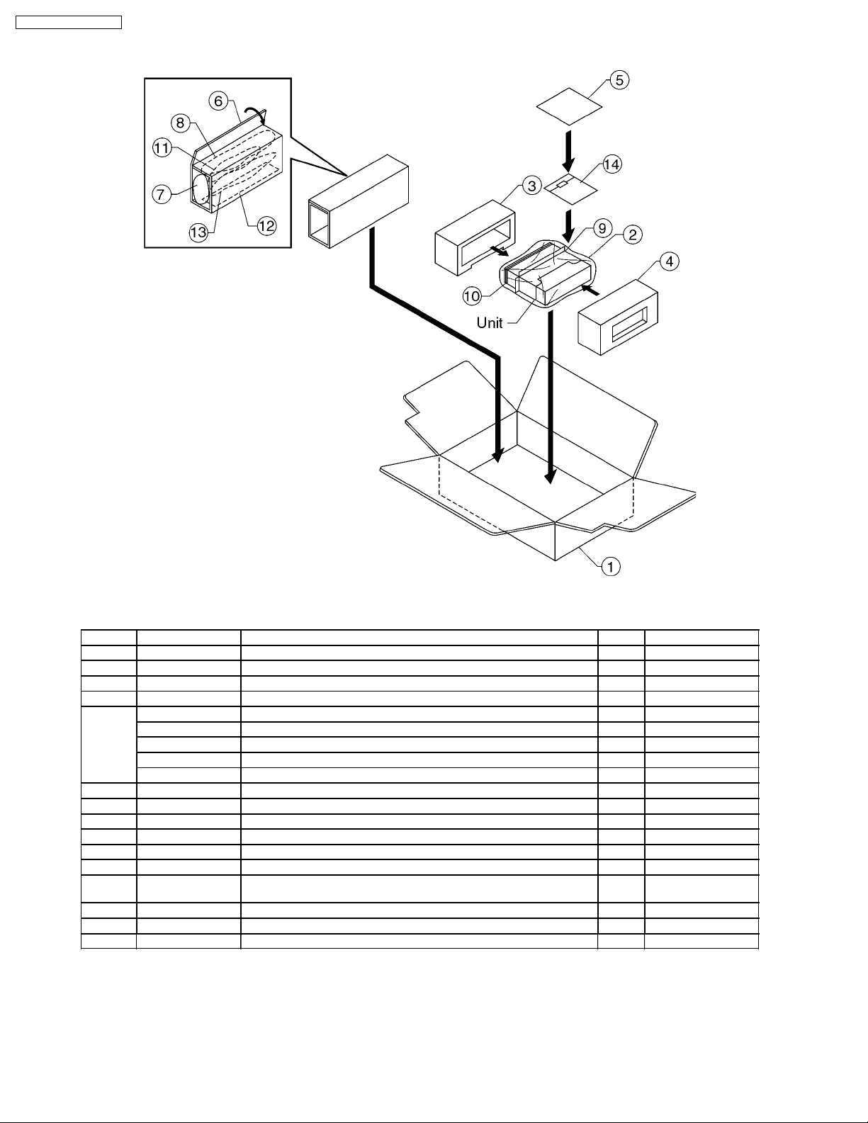
12 PACKING PARTS LIST
· Item numbers listed below should not order regular spare parts. (not available)
Item No. Part No. Part Name & Description Q´ty Remarks
1 - Inner Carton 1 Not available
2 - Polyethylene Bag 1 Not available
3 - Packing Pad Front 1 Not available
4 - Packing Pad Rear 1 Not available
5 - Instruction Kit 1 Not available
- Operating Instructions (1) Not available
- System Upgrade Guidebook (1) Not available
- Installation Instructions (1) Not available
- Owners Information Card (1) Not available
6 - Sleeve 1 Not available
7 EUR7641010 Remote Control Unit (includes a battery) 1
- CR2025/1F Lithium Battery 1
8 YGAJ021009 Power Connector 1
9 YEFX0217222 Mounting Collar 1
10 YEFC051013 Trim Plate 1
11 YEP0FZ5701 Installation Kit (Lock Cancel Plate, Mounting Bolt, Tapping Screw, Hex
Nut)
12 YEFG04019 Rear Support Strap 1
13 YEFA134150 Removable Face Plate Case 1
14 YEP0FZ5702 Security Screw Kit 1
1
16
13 REPLACEMENT PARTS
LIST [CQ-C7413U]
Notes :
1. Be sure to make your orders of replacement parts
according to this list.
2. Important safety notice: Components, identified by
have special characteristics important for safety. When
replacing any of these components, use only
manufacturer´s specified parts.
3. Location keys in the remarks column indicates the general
location of the parts shown in the exploded drawing, as in a
road map.
4. The marking (RTL) indicates that Retention Time is limited
for this item. After the discontinuation of assembly in
production, the item will continue to be available for a
specific period of time. The retention period of availability is
dependent on the type of assembly, and in accordance with
the laws governing part and product retention. After the end
of this period, the assembly will no longer be available.
5. Reference materials of parts with the “TSN“ mark in the
remarks column are uploaded in the TSN (Technical
Service Navigation) system website. Please download from
that website for references.
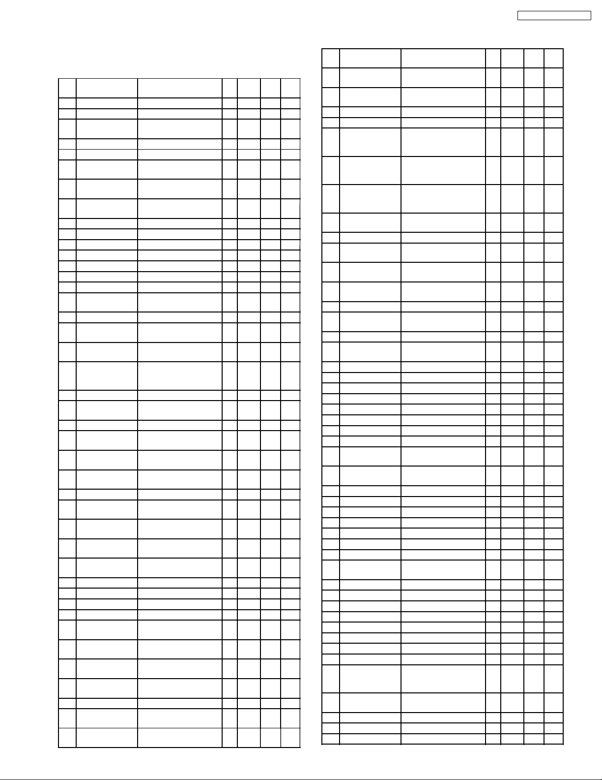
Ref. No. Part No. Part Name & Description Remarks
[E3108] Main/Sub Block
IC´s AND TRANSISTORs
IC201 C1BB00000796 IC
IC221 C1BB00001131 IC
IC231 C0JBZS000003 IC
IC251 C0ABBA000221 IC
IC252 C0ABCA000121 IC
IC271 C1ZAZ0001450 IC
IC401 C1BB00001045 IC
IC601 C2CBKG000035 IC
IC630 C0JBAA000372 IC
IC650 C0JBAA000372 IC
IC670 YEAMC14584BE IC
IC701 C0DAZHF00004 IC
IC702 C0EBZ0000035 IC
IC730 C0DAEKG00002 IC
IC752 C0CBCBG00012 IC
IC755 C0DBZGD00040 IC
IC760 C0GBG0000032 IC
IC770 C0DBAHG00020 IC
IC790 C0CBCYG00004 IC
PA51 C5BA00000122 Electronic Tuner
Q55 B1GDGFEH0001 Transistor
Q56 B1AAEC000002 Transistor
Q220 B1GBCFNN0004 Transistor
Q235 B1GBHBEA0004 Transistor
Q241 B1GBHBEA0004 Transistor
Q251 B1GBHBEA0004 Transistor
Q252 B1GBHBEA0004 Transistor
Q320 B1GBCFNN0004 Transistor
Q335 B1GBHBEA0004 Transistor
Q341 B1GBHBEA0004 Transistor
Q351 B1GBHBEA0004 Transistor
Q352 B1GBHBEA0004 Transistor
Q353 B1GBHBEA0004 Transistor
Q354 B1GDCFJJ0002 Transistor
Q371 B1GBCFNN0004 Transistor
Q372 YEANC114YKX Transistor
Q376 B1GBCFNN0004 Transistor
Q411 B1CBGF000005 Transistor
Q630 B1GBCFNN0004 Transistor
Q633 B1GDCFJJ0002 Transistor
mark
CQ-C7413U / CQ-C7113U
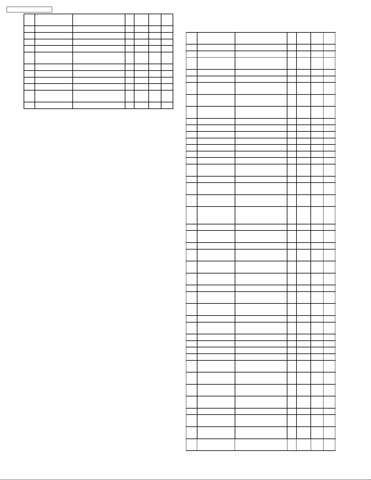
Ref. No. Part No. Part Name & Description Remarks
Q650 YEANC114YKX Transistor
Q651 YEANC114YKX Transistor
Q652 YEANC114YKX Transistor
Q680 B1GDGFEH0001 Transistor
Q681 B1GDCFJJ0002 Transistor
Q701 B1BACF000026 Transistor
Q760 B1GBCFNN0004 Transistor
Q771 B1ABCF000187 Transistor
Q791 B1GBNCEJ0003 Transistor
Q793 YEANC114YKX Transistor
DIODEs
D201 B0JCME000012 Diode
D202 B0JCME000012 Diode
D203 B0JCME000012 Diode
D204 B0JCME000012 Diode
D251 B0JCMC000004 Diode
D301 B0JCME000012 Diode
D302 B0JCME000012 Diode
D303 B0JCME000012 Diode
D304 B0JCME000012 Diode
D601 B0JCMC000004 Diode
D630 B3AAB0000143 Diode
D631 B0BC5R600003 Diode
D632 MA152WATX Diode
D635 B0BC5R600003 Diode
D636 B0BC5R600003 Diode
D637 B0BC5R600003 Diode
D638 B0BC5R600003 Diode
D639 B0BC5R600003 Diode
D670 B0JCMC000004 Diode
D672 B0JCMC000004 Diode
D673 B0BC5R000020 Diode
D701 YEADDAM3MA47 Diode
D702 MA736TX Diode
D703 B0BC5R7A0062 Diode
D704 B0JCMC000004 Diode
D705 YEADSR1544TL Diode
D706 YEADSR1544TL Diode
D707 YEADRB051L40 Diode
D708 MA736TX Diode
D710 B0JCMC000004 Diode
D715 MA3X152A0L Diode
D716 MA721TX Diode
D751 YEADSR1544TL Diode
D752 YEADSR1544TL Diode
D760 B0BC5R000020 Diode
D761 B0BC3R0A0058 Diode
D770 B0JCMC000004 Diode
D771 B0JCQD000002 Diode
D772 B0BC013A0063 Diode
CAPACITORs
C52 YECUS1H470JC Ceramic, 47PF 50WV
C53 F1J1H103A513 Ceramic, 0.01µF 50WV
C54 F2A1A221A449 Electrolytic, 220µF 10WV
C55 F1J1H103A513 Ceramic, 0.01µF 50WV
C56 F3F1E105A001 Tantalum, 1µF 25WV
C57 F2A1A101A450 Electrolytic, 100µF 10WV
C61 YECUS1E273KX Ceramic, 0.027µF 25WV
C62 YECUS1E273KX Ceramic, 0.027µF 25WV
C65 F1J1H1020024 Ceramic, 1000PF 50WV
C206 F2A1C100A502 Electrolytic, 10µF 16WV
C213 F1J1A2250004 Ceramic, 2.2µF 10WV
C215 F1J1A2250004 Ceramic, 2.2µF 10WV
C217 YECUS1C334KX Ceramic, 0.33µF 16WV
C220 F1J1C225A138 Ceramic, 2.2µF 16WV
C237 F1J1C225A138 Ceramic, 2.2µF 16WV
C242 F1J1C225A138 Ceramic, 2.2µF 16WV
C251 YECUS1C474KX Ceramic, 0.47µF 16WV
C252 YECUS1H470JM Ceramic, 47PF 50WV
C253 F1J1C225A138 Ceramic, 2.2µF 16WV
17
CQ-C7413U / CQ-C7113U
Ref. No. Part No. Part Name & Description Remarks
C254 YECUS1C474KX Ceramic, 0.47µF 16WV
C255 YECUS1H470JM Ceramic, 47PF 50WV
C256 F1J1C225A138 Ceramic, 2.2µF 16WV
C271 F1J1H472A675 Ceramic, 4700PF 50WV
C272 F1J1H472A675 Ceramic, 4700PF 50WV
C274 F2A1C470A630 Electrolytic, 47µF 16WV
C275 F1J1C1050013 Ceramic, 1µF 16WV
C278 YECUS1E104ZF Ceramic, 0.1µF 25WV
C279 F2A1C4720027 Electrolytic, 4700µF 16WV
C281 F1K1C1060001 Ceramic, 10µF 16WV
C282 YECUZ1C104KX Ceramic, 0.1µF 16WV
C283 F1K1C1060001 Ceramic, 10µF 16WV
C296 F1K1C4740009 Ceramic, 0.47µF 16WV
C297 F1K1C4740009 Ceramic, 0.47µF 16WV
C306 F2A1C100A502 Electrolytic, 10µF 16WV
C313 F1J1A2250004 Ceramic, 2.2µF 10WV
C315 F1J1A2250004 Ceramic, 2.2µF 10WV
C317 YECUS1C334KX Ceramic, 0.33µF 16WV
C320 F1J1C225A138 Ceramic, 2.2µF 16WV
C321 F1J1C225A138 Ceramic, 2.2µF 16WV
C323 F2A1C100A502 Electrolytic, 10µF 16WV
C324 F2A1H2R2A634 Electrolytic, 2.2µF 50WV
C325 F2A1H2R2A634 Electrolytic, 2.2µF 50WV
C326 F1J1A2250004 Ceramic, 2.2µF 10WV
C327 F2A1A221A449 Electrolytic, 220µF 10WV
C328 F1J1H103A513 Ceramic, 0.01µF 50WV
C330 F1J1A2250004 Ceramic, 2.2µF 10WV
C331 F1J1C225A138 Ceramic, 2.2µF 16WV
C332 YECUZ1C104KX Ceramic, 0.1µF 16WV
C333 F1H1E103A011 Ceramic, 0.01µF 25WV
C334 YECUZ1C104KX Ceramic, 0.1µF 16WV
C335 YECUZ1C104KX Ceramic, 0.1µF 16WV
C336 YECUZ1C104KX Ceramic, 0.1µF 16WV
C337 YECUZ1C104KX Ceramic, 0.1µF 16WV
C338 YECUZ1C104KX Ceramic, 0.1µF 16WV
C339 YECUZ1C104KX Ceramic, 0.1µF 16WV
C340 F1J1C1050013 Ceramic, 1µF 16WV
C341 F1K1C1060001 Ceramic, 10µF 16WV
C342 YECUZ1C333KX Ceramic, 0.033µF 16WV
C343 F1H1E103A011 Ceramic, 0.01µF 25WV
C344 YECUS1C334KX Ceramic, 0.33µF 16WV
C346 YECUS1C474KX Ceramic, 0.47µF 16WV
C347 YECUZ1H221JC Ceramic, 220PF 50WV
C351 YECUS1C474KX Ceramic, 0.47µF 16WV
C352 YECUS1H470JM Ceramic, 47PF 50WV
C353 F1J1C225A138 Ceramic, 2.2µF 16WV
C354 YECUS1C474KX Ceramic, 0.47µF 16WV
C355 YECUS1H470JM Ceramic, 47PF 50WV
C356 F1J1C225A138 Ceramic, 2.2µF 16WV
C361 YECUS1C474KX Ceramic, 0.47µF 16WV
C362 YECUS1H470JM Ceramic, 47PF 50WV
C363 ECEA1EKS3R3I Electrolytic, 3.3µF 25WV
C364 F2A1C100A502 Electrolytic, 10µF 16WV
C365 YECUS1C104KX Ceramic, 0.1µF 16WV
C366 YECUS1C104KX Ceramic, 0.1µF 16WV
C367 YECUS1C104KX Ceramic, 0.1µF 16WV
C368 F2A1C470A630 Electrolytic, 47µF 16WV
C371 F1J1H472A675 Ceramic, 4700PF 50WV
C372 F1J1H472A675 Ceramic, 4700PF 50WV
C374 F2A1H2R20044 Electrolytic, 2.2µF 50WV
C375 F2A1C100A502 Electrolytic, 10µF 16WV
C378 YECUS1E104ZF Ceramic, 0.1µF 25WV
C381 F1K1C1060001 Ceramic, 10µF 16WV
C382 YECUZ1C104KX Ceramic, 0.1µF 16WV
C383 F1K1C1060001 Ceramic, 10µF 16WV
C384 F2A1A101A450 Electrolytic, 100µF 10WV
C385 F1K1C1060001 Ceramic, 10µF 16WV
C386 F1K1C1060001 Ceramic, 10µF 16WV
C387 F1K1C1060001 Ceramic, 10µF 16WV
C388 F1K1C1060001 Ceramic, 10µF 16WV
C389 F1K1C1060001 Ceramic, 10µF 16WV
C396 F1K1C4740009 Ceramic, 0.47µF 16WV
C397 F1K1C4740009 Ceramic, 0.47µF 16WV
C401 F1J1H120A034 Ceramic, 12PF 50WV
Ref. No. Part No. Part Name & Description Remarks
C402 F1J1H120A034 Ceramic, 12PF 50WV
C403 F2A0J101A500 Electrolytic, 100µF 6.3WV
C404 F1J1H103A513 Ceramic, 0.01µF 50WV
C405 F1H1H101A231 Ceramic, 100PF 50WV
C411 F1J1H103A513 Ceramic, 0.01µF 50WV
C412 YECUS1E223KX Ceramic, 0.022µF 25WV
C413 ECQV1H224JL2 Plastic Film, 0.22µF 50WV
C414 F2A1A221A449 Electrolytic, 220µF 10WV
C601 YECUS1C104KX Ceramic, 0.1µF 16WV
C602 F1H1E103A011 Ceramic, 0.01µF 25WV
C603 F2A0J3310051 Electrolytic, 330µF 6.3WV
C604 ECA0JM471I Electrolytic, 470µF 6.3WV
C605 YECUS1C104KX Ceramic, 0.1µF 16WV
C606 F1H1H2200008 Ceramic, 22PF 50WV
C607 YECUS1H220JC Ceramic, 22PF 50WV
C608 YECUS1C104KX Ceramic, 0.1µF 16WV
C609 F1J1A106A023 Ceramic, 10µF 10WV
C610 YECUS1C104KX Ceramic, 0.1µF 16WV
C612 F1H1H120A231 Ceramic, 12PF 50WV
C613 F1H1H100A226 Ceramic, 10PF 50WV
C631 F2A1H4R7A632 Electrolytic, 4.7µF 50WV
C632 YECUS1E104ZF Ceramic, 0.1µF 25WV
C633 F2A1C470A630 Electrolytic, 47µF 16WV
C634 F1H1E103A011 Ceramic, 0.01µF 25WV
C635 F1J1H103A513 Ceramic, 0.01µF 50WV
C650 F1J1H103A513 Ceramic, 0.01µF 50WV
C670 F2A1C100A502 Electrolytic, 10µF 16WV
C671 F1H1E103A011 Ceramic, 0.01µF 25WV
C680 F2A1H2R2A634 Electrolytic, 2.2µF 50WV
C701 YECUS1C154KX Ceramic, 0.15µF 16WV
C702 F2A1C1020069 Electrolytic, 1000µF 16WV
C704 F2A0J3310051 Electrolytic, 330µF 6.3WV
C705 F1H1E103A011 Ceramic, 0.01µF 25WV
C707 F2A1C1020069 Electrolytic, 1000µF 16WV
C708 F2A1H1R00095 Electrolytic, 1µF 50WV
C713 YECUS1C474KX Ceramic, 0.47µF 16WV
C715 YECUS1E104ZF Ceramic, 0.1µF 25WV
C716 YECUS1C104KX Ceramic, 0.1µF 16WV
C717 YECUS1C104KX Ceramic, 0.1µF 16WV
C718 YECUS1E104ZF Ceramic, 0.1µF 25WV
C719 EEAFC1A820H Electrolytic, 82µF 10WV
C720 YECUS1C104KX Ceramic, 0.1µF 16WV
C721 YECUS1C104KX Ceramic, 0.1µF 16WV
C730 F1K1E334A022 Ceramic, 0.33µF 25WV
C731 YECUX1C334KX Ceramic, 0.33µF 16WV
C732 EEAFC1C560H Electrolytic, 56µF 16WV
C752 YECUS1C334KX Ceramic, 0.33µF 16WV
C753 YECUS1C334KX Ceramic, 0.33µF 16WV
C754 EEAFC0J560H Electrolytic, 56µF 6.3WV
C755 YECUZ1C104KX Ceramic, 0.1µF 16WV
C756 F1J1C1050013 Ceramic, 1µF 16WV
C757 F1H1E103A011 Ceramic, 0.01µF 25WV
C758 F2A0J470A558 Electrolytic, 47µF 6.3WV
C760 F1H1E103A011 Ceramic, 0.01µF 25WV
C761 YECUS1E104ZF Ceramic, 0.1µF 25WV
C762 F2A1C470A630 Electrolytic, 47µF 16WV
C763 YECUS1E104ZF Ceramic, 0.1µF 25WV
C771 F2A1C1010089 Electrolytic, 100µF 16WV
C772 YECUS1C104KX Ceramic, 0.1µF 16WV
C773 F1J1H271A025 Ceramic, 270PF 50WV
C774 EEEFK1E101P Electrolytic, 100µF 25WV
C775 YECUZ1C104KX Ceramic, 0.1µF 16WV
C776 F2A1E101A575 Electrolytic, 100µF 25WV
C777 F1J1H103A513 Ceramic, 0.01µF 50WV
C778 F2A1C100A502 Electrolytic, 10µF 16WV
C791 EEAFC1C560H Electrolytic, 56µF 16WV
C792 YECUX1C334KX Ceramic, 0.33µF 16WV
C793 F1J1E334A009 Ceramic, 0.33µF 25WV
C797 YECUS1C104KX Ceramic, 0.1µF 16WV
RESISTORs
J401 ERJ6GEY0R00V Chip, 0Ω 1/10W
J403 ERJ8GEY0R00V Chip, 0Ω 1/8W
18
Ref. No. Part No. Part Name & Description Remarks
J404 ERJ6GEY0R00V Chip, 0Ω 1/10W
J474 ERJ8GX0R00V Chip, 0Ω 1/8W
J475 ERJ8GX0R00V Chip, 0Ω 1/8W
J476 ERJ8GX0R00V Chip, 0Ω 1/8W
J477 ERJ8GX0R00V Chip, 0Ω 1/8W
J478 ERJ8GX0R00V Chip, 0Ω 1/8W
J479 ERJ8GX0R00V Chip, 0Ω 1/8W
J480 ERJ8GX0R00V Chip, 0Ω 1/8W
J481 ERJ8GX0R00V Chip, 0Ω 1/8W
J482 ERJ8GX0R00V Chip, 0Ω 1/8W
J483 ERJ8GX0R00V Chip, 0Ω 1/8W
J501 ERJ8GEY0R00V Chip, 0Ω 1/8W
J502 ERJ8GEY0R00V Chip, 0Ω 1/8W
J503 ERJ8GEY0R00V Chip, 0Ω 1/8W
J504 ERJ8GEY0R00V Chip, 0Ω 1/8W
J506 ERJ8GEY0R00V Chip, 0Ω 1/8W
J507 ERJ8GEY0R00V Chip, 0Ω 1/8W
J508 ERJ8GEY0R00V Chip, 0Ω 1/8W
J509 ERJ8GEY0R00V Chip, 0Ω 1/8W
J510 ERJ8GEY0R00V Chip, 0Ω 1/8W
J511 ERJ8GEY0R00V Chip, 0Ω 1/8W
J512 ERJ8GEY0R00V Chip, 0Ω 1/8W
J513 ERJ8GEY0R00V Chip, 0Ω 1/8W
J514 ERJ8GEY0R00V Chip, 0Ω 1/8W
J515 ERJ8GEY0R00V Chip, 0Ω 1/8W
J516 ERJ8GEY0R00V Chip, 0Ω 1/8W
J523 ERJ8GX0R00V Chip, 0Ω 1/8W
J524 ERJ8GX0R00V Chip, 0Ω 1/8W
J525 ERJ8GX0R00V Chip, 0Ω 1/8W
J526 ERJ8GX0R00V Chip, 0Ω 1/8W
J529 ERJ8GX0R00V Chip, 0Ω 1/8W
J531 ERJ8GX0R00V Chip, 0Ω 1/8W
J534 ERJ8GX0R00V Chip, 0Ω 1/8W
J536 ERJ8GX0R00V Chip, 0Ω 1/8W
J537 ERJ8GX0R00V Chip, 0Ω 1/8W
J538 ERJ8GX0R00V Chip, 0Ω 1/8W
J539 ERJ8GX0R00V Chip, 0Ω 1/8W
J540 ERJ8GX0R00V Chip, 0Ω 1/8W
J542 ERJ8GX0R00V Chip, 0Ω 1/8W
J544 ERJ8GX0R00V Chip, 0Ω 1/8W
J545 ERJ8GX0R00V Chip, 0Ω 1/8W
J546 ERJ8GX0R00V Chip, 0Ω 1/8W
J550 ERJ8GX0R00V Chip, 0Ω 1/8W
J551 ERJ8GX0R00V Chip, 0Ω 1/8W
J552 ERJ8GX0R00V Chip, 0Ω 1/8W
J553 ERJ8GX0R00V Chip, 0Ω 1/8W
J554 ERJ8GX0R00V Chip, 0Ω 1/8W
J555 ERJ8GEY0R00V Chip, 0Ω 1/8W
J556 ERJ8GX0R00V Chip, 0Ω 1/8W
J557 ERJ8GX0R00V Chip, 0Ω 1/8W
J560 ERJ8GEY0R00V Chip, 0Ω 1/8W
J561 ERJ8GEY0R00V Chip, 0Ω 1/8W
J563 ERJ8GX0R00V Chip, 0Ω 1/8W
J565 ERJ8GX0R00V Chip, 0Ω 1/8W
J570 ERJ8GX0R00V Chip, 0Ω 1/8W
J571 ERJ8GX0R00V Chip, 0Ω 1/8W
J573 ERJ8GX0R00V Chip, 0Ω 1/8W
J579 ERJ8GEY0R00V Chip, 0Ω 1/8W
J580 ERJ8GX0R00V Chip, 0Ω 1/8W
J582 ERJ8GEY0R00V Chip, 0Ω 1/8W
J583 ERJ8GEY0R00V Chip, 0Ω 1/8W
J590 ERJ8GEY0R00V Chip, 0Ω 1/8W
J591 ERJ6GEY0R00V Chip, 0Ω 1/10W
J592 ERJ8GX0R00V Chip, 0Ω 1/8W
R50 ERJ6GEYJ5R6V Chip, 5.6Ω 1/10W
R54 ERJ6GEYJ101 Chip, 100Ω 1/10W
R55 ERJ6GEYJ221 Chip, 220Ω 1/10W
R56 ERJ6GEYJ102 Chip, 1kΩ 1/10W
R59 ERJ3GEYJ104V Chip, 100kΩ 1/16W
R65 ERJ6GEYJ393 Chip, 39kΩ 1/10W
R202 ERJ6GEYJ152 Chip, 1.5kΩ 1/10W
R203 ERJ6GEYJ103 Chip, 10kΩ 1/10W
R213 ERJ6GEYJ562 Chip, 5.6kΩ 1/10W
R214 ERJ6GEYJ103 Chip, 10kΩ 1/10W
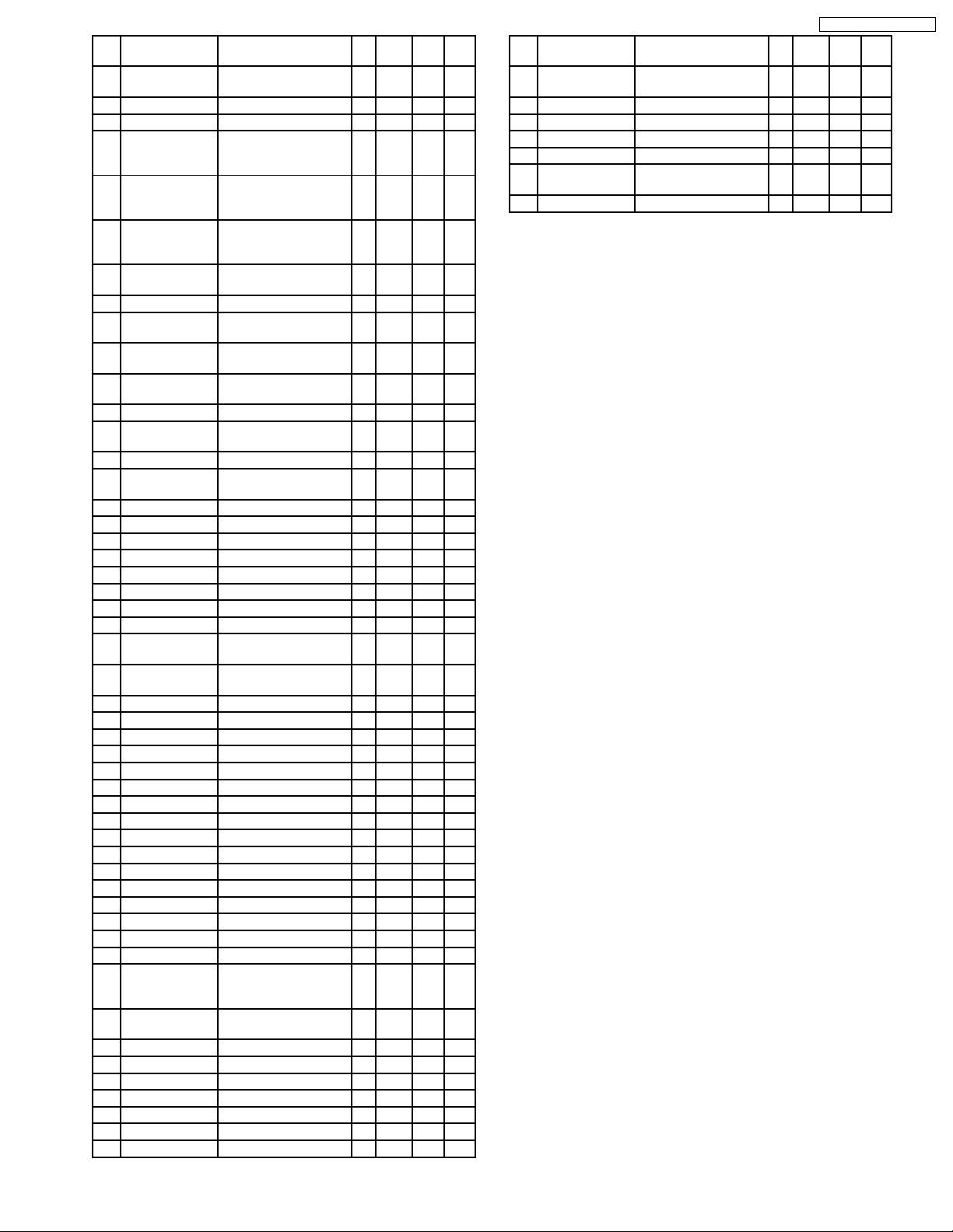
CQ-C7413U / CQ-C7113U
Ref. No. Part No. Part Name & Description Remarks
R215 ERJ3GEYJ472V Chip, 4.7kΩ 1/16W
R216 ERJ3GEYJ123V Chip, 12kΩ 1/16W
R217 ERJ3GEYJ183V Chip, 18kΩ 1/16W
R220 ERJ3GEYJ750V Chip, 75Ω 1/16W
R221 ERJ3GEYJ153V Chip, 15kΩ 1/16W
R235 ERJ3GEYJ104V Chip, 100kΩ 1/16W
R237 ERJ3GEYJ271V Chip, 270Ω 1/16W
R241 ERJ3GEYJ104V Chip, 100kΩ 1/16W
R242 ERJ3GEYJ271V Chip, 270Ω 1/16W
R251 ERJ3GEYJ104V Chip, 100kΩ 1/16W
R252 ERJ3GEYJ393V Chip, 39kΩ 1/16W
R253 ERJ3GEYJ433V Chip, 43kΩ 1/16W
R254 ERJ3GEYJ560V Chip, 56Ω 1/16W
R255 ERJ3GEYJ104V Chip, 100kΩ 1/16W
R256 ERJ3GEYJ104V Chip, 100kΩ 1/16W
R257 ERJ3GEYJ393V Chip, 39kΩ 1/16W
R258 ERJ3GEYJ433V Chip, 43kΩ 1/16W
R259 ERJ3GEYJ560V Chip, 56Ω 1/16W
R260 ERJ6GEYJ104 Chip, 100kΩ 1/10W
R275 ERJ8GEYJ223V Chip, 22kΩ 1/8W
R281 ERJ3GEYJ104V Chip, 100kΩ 1/16W
R282 ERJ3GEYJ104V Chip, 100kΩ 1/16W
R283 ERJ3GEYJ103V Chip, 10kΩ 1/16W
R284 ERJ3GEYJ103V Chip, 10kΩ 1/16W
R285 ERJ3GEYJ272V Chip, 2.7kΩ 1/16W
R286 ERJ3GEYJ102V Chip, 1kΩ 1/16W
R291 ERJ3GEYJ104V Chip, 100kΩ 1/16W
R296 ERJ6GEYJ271 Chip, 270Ω 1/10W
R297 ERJ6GEYJ271 Chip, 270Ω 1/10W
R298 ERJ3GEYJ222V Chip, 2.2kΩ 1/16W
R302 ERJ3GEYJ152V Chip, 1.5kΩ 1/16W
R303 ERJ3GEYJ103V Chip, 10kΩ 1/16W
R313 ERJ6GEYJ562 Chip, 5.6kΩ 1/10W
R314 ERJ6GEYJ103 Chip, 10kΩ 1/10W
R315 ERJ3GEYJ472V Chip, 4.7kΩ 1/16W
R316 ERJ3GEYJ123V Chip, 12kΩ 1/16W
R317 ERJ3GEYJ183V Chip, 18kΩ 1/16W
R320 ERJ3GEYJ750V Chip, 75Ω 1/16W
R321 ERJ3GEYJ153V Chip, 15kΩ 1/16W
R323 ERJ3GEYJ102V Chip, 1kΩ 1/16W
R324 ERJ3GEYJ103V Chip, 10kΩ 1/16W
R325 ERJ6GEYJ102 Chip, 1kΩ 1/10W
R326 ERJ6GEYJ101 Chip, 100Ω 1/10W
R327 ERJ6GEYJ823 Chip, 82kΩ 1/10W
R330 ERJ6GEYJ221 Chip, 220Ω 1/10W
R335 ERJ3GEYJ104V Chip, 100kΩ 1/16W
R336 ERJ3GEYJ271V Chip, 270Ω 1/16W
R341 ERJ3GEYJ104V Chip, 100kΩ 1/16W
R342 ERJ3GEYJ271V Chip, 270Ω 1/16W
R351 ERJ3GEYJ104V Chip, 100kΩ 1/16W
R352 ERJ3GEYJ393V Chip, 39kΩ 1/16W
R353 ERJ3GEYJ433V Chip, 43kΩ 1/16W
R354 ERJ3GEYJ560V Chip, 56Ω 1/16W
R355 ERJ3GEYJ104V Chip, 100kΩ 1/16W
R356 ERJ3GEYJ104V Chip, 100kΩ 1/16W
R357 ERJ3GEYJ393V Chip, 39kΩ 1/16W
R358 ERJ3GEYJ433V Chip, 43kΩ 1/16W
R359 ERJ3GEYJ560V Chip, 56Ω 1/16W
R360 ERJ3GEYJ104V Chip, 100kΩ 1/16W
R361 ERJ6GEYJ104 Chip, 100kΩ 1/10W
R362 ERJ6GEYJ393 Chip, 39kΩ 1/10W
R363 ERJ6GEYJ393 Chip, 39kΩ 1/10W
R364 ERJ6GEYJ560 Chip, 56Ω 1/10W
R365 ERJ6GEYJ104 Chip, 100kΩ 1/10W
R366 ERJ6GEYJ103 Chip, 10kΩ 1/10W
R367 ERJ6GEYJ103 Chip, 10kΩ 1/10W
R368 ERJ3GEYJ563V Chip, 56kΩ 1/16W
R369 ERJ3GEYJ133V Chip, 13kΩ 1/16W
R370 ERJ3GEYJ363V Chip, 36kΩ 1/16W
R371 ERJ3GEYJ822V Chip, 8.2kΩ 1/16W
R372 ERJ3GEYJ103V Chip, 10kΩ 1/16W
R373 ERJ6GEYJ183 Chip, 18kΩ 1/10W
R374 ERJ3GEYJ164V Chip, 160kΩ 1/16W
R375 ERJ6GEYJ562 Chip, 5.6kΩ 1/10W
19
CQ-C7413U / CQ-C7113U
Ref. No. Part No. Part Name & Description Remarks
R376 ERJ3GEYJ103V Chip, 10kΩ 1/16W
R377 ERJ3GEYJ104V Chip, 100kΩ 1/16W
R378 ERJ3GEY0R00V Chip, 0Ω 1/16W
R379 ERJ3GEYJ472V Chip, 4.7kΩ 1/16W
R381 ERJ3GEYJ104V Chip, 100kΩ 1/16W
R382 ERJ3GEYJ104V Chip, 100kΩ 1/16W
R383 ERJ3GEYJ103V Chip, 10kΩ 1/16W
R384 ERJ3GEYJ103V Chip, 10kΩ 1/16W
R385 ERJ3GEYJ272V Chip, 2.7kΩ 1/16W
R386 ERJ3GEYJ102V Chip, 1kΩ 1/16W
R387 ERJ6GEYJ103 Chip, 10kΩ 1/10W
R388 ERJ6GEYJ103 Chip, 10kΩ 1/10W
R389 ERJ6GEYJ103 Chip, 10kΩ 1/10W
R390 ERJ3GEYJ473V Chip, 47kΩ 1/16W
R391 ERJ3GEYJ104V Chip, 100kΩ 1/16W
R392 ERJ6GEYJ104 Chip, 100kΩ 1/10W
R393 ERJ3GEYJ104V Chip, 100kΩ 1/16W
R396 ERJ6GEYJ271 Chip, 270Ω 1/10W
R397 ERJ6GEYJ271 Chip, 270Ω 1/10W
R398 ERJ3GEYJ222V Chip, 2.2kΩ 1/16W
R401 ERJ3GEYJ152V Chip, 1.5kΩ 1/16W
R402 ERJ3GEYJ472V Chip, 4.7kΩ 1/16W
R403 ERJ3GEYJ473V Chip, 47kΩ 1/16W
R404 ERJ3GEYJ102V Chip, 1kΩ 1/16W
R405 ERJ3GEYJ102V Chip, 1kΩ 1/16W
R406 ERJ3GEYJ102V Chip, 1kΩ 1/16W
R407 ERJ3GEYJ102V Chip, 1kΩ 1/16W
R408 ERJ3GEYJ473V Chip, 47kΩ 1/16W
R409 ERJ3GEYJ102V Chip, 1kΩ 1/16W
R410 ERJ3GEY0R00V Chip, 0Ω 1/16W
R411 ERJ3GEYJ221V Chip, 220Ω 1/16W
R413 ERJ6GEYJ182 Chip, 1.8kΩ 1/10W
R414 ERJ8GEYJ561V Chip, 560Ω 1/8W
R417 ERJ3GEYJ100V Chip, 10Ω 1/16W
R600 ERJ8GX0R00V Chip, 0Ω 1/8W
R601 ERJ3GEYJ432V Chip, 4.3kΩ 1/16W
R602 ERJ3GEYJ432V Chip, 4.3kΩ 1/16W
R603 ERJ6GEYJ103 Chip, 10kΩ 1/10W
R604 ERJ6GEYJ103 Chip, 10kΩ 1/10W
R605 ERJ3GEYJ102V Chip, 1kΩ 1/16W
R607 ERJ3GEYJ333V Chip, 33kΩ 1/16W
R608 ERJ3GEYJ822V Chip, 8.2kΩ 1/16W
R609 ERJ3GEYJ473V Chip, 47kΩ 1/16W
R611 ERJ3GEYJ683V Chip, 68kΩ 1/16W
R612 ERJ3GEYJ153V Chip, 15kΩ 1/16W
R613 ERJ3GEYJ103V Chip, 10kΩ 1/16W
R614 ERJ3GEYJ103V Chip, 10kΩ 1/16W
R615 ERJ6GEYJ103 Chip, 10kΩ 1/10W
R616 ERJ3GEYJ684V Chip, 680kΩ 1/16W
R617 ERJ3GEYJ103V Chip, 10kΩ 1/16W
R618 ERJ3GEYJ223V Chip, 22kΩ 1/16W
R619 ERJ3GEYJ473V Chip, 47kΩ 1/16W
R620 ERJ3GEYJ103V Chip, 10kΩ 1/16W
R621 ERJ3GEYJ472V Chip, 4.7kΩ 1/16W
R622 ERJ6GEYJ473 Chip, 47kΩ 1/10W
R624 ERJ3GEYJ104V Chip, 100kΩ 1/16W
R625 ERJ3GEYJ473V Chip, 47kΩ 1/16W
R626 ERJ6GEYJ102 Chip, 1kΩ 1/10W
R627 ERJ3GEYJ103V Chip, 10kΩ 1/16W
R628 ERJ3GEYJ103V Chip, 10kΩ 1/16W
R629 ERJ8GEYJ104V Chip, 100kΩ 1/8W
R631 ERJ6GEYJ821 Chip, 820Ω 1/10W
R632 ERJ6GEYJ473 Chip, 47kΩ 1/10W
R634 ERJ6GEYJ561 Chip, 560Ω 1/10W
R638 ERJ3GEYJ102V Chip, 1kΩ 1/16W
R639 ERJ3GEYJ102V Chip, 1kΩ 1/16W
R640 ERJ6GEYJ561 Chip, 560Ω 1/10W
R641 ERJ3GEYJ102V Chip, 1kΩ 1/16W
R646 ERJ3GEYJ104V Chip, 100kΩ 1/16W
R653 ERJ3GEYJ512V Chip, 5.1kΩ 1/16W
R654 ERJ6GEYJ512V Chip, 5.1kΩ 1/10W
R655 ERJ6GEYJ103 Chip, 10kΩ 1/10W
R656 ERJ6GEYJ272 Chip, 2.7kΩ 1/10W
R657 ERJ3GEYJ272V Chip, 2.7kΩ 1/16W
Ref. No. Part No. Part Name & Description Remarks
R658 ERJ6GEYJ473 Chip, 47kΩ 1/10W
R659 ERJ6GEYJ272 Chip, 2.7kΩ 1/10W
R660 ERJ6GEYJ272 Chip, 2.7kΩ 1/10W
R661 ERJ6GEYJ473 Chip, 47kΩ 1/10W
R662 ERJ3GEYJ472V Chip, 4.7kΩ 1/16W
R663 ERJ6GEYJ512V Chip, 5.1kΩ 1/10W
R664 ERJ6GEYJ512V Chip, 5.1kΩ 1/10W
R670 ERJ3GEYJ104V Chip, 100kΩ 1/16W
R671 ERJ3GEYJ104V Chip, 100kΩ 1/16W
R673 ERJ3GEYJ104V Chip, 100kΩ 1/16W
R674 ERJ3GEYJ272V Chip, 2.7kΩ 1/16W
R675 ERJ6GEYJ272 Chip, 2.7kΩ 1/10W
R676 ERJ3GEYJ472V Chip, 4.7kΩ 1/16W
R677 ERJ6GEYJ561 Chip, 560Ω 1/10W
R678 ERJ3GEYJ104V Chip, 100kΩ 1/16W
R680 ERJ6GEYJ271 Chip, 270Ω 1/10W
R681 ERJ6GEYJ562 Chip, 5.6kΩ 1/10W
R682 ERJ3GEYJ473V Chip, 47kΩ 1/16W
R684 ERJ6GEYJ561 Chip, 560Ω 1/10W
R685 ERJ3GEYJ561V Chip, 560Ω 1/16W
R686 ERJ3GEYJ561V Chip, 560Ω 1/16W
R687 ERJ6GEYJ561 Chip, 560Ω 1/10W
R688 ERJ6GEYJ561 Chip, 560Ω 1/10W
R689 ERJ3GEYJ561V Chip, 560Ω 1/16W
R690 ERJ3GEYJ561V Chip, 560Ω 1/16W
R701 ERJ6GEYJ102 Chip, 1kΩ 1/10W
R702 ERJ3GEYJ224V Chip, 220kΩ 1/16W
R703 ERJ6GEYJ473 Chip, 47kΩ 1/10W
R704 ERJ8GEYJ4R7V Chip, 4.7Ω 1/8W
R705 ERJ6GEYJ682 Chip, 6.8kΩ 1/10W
R715 ERJ3GEYJ472V Chip, 4.7kΩ 1/16W
R716 ERJ6GEYJ473 Chip, 47kΩ 1/10W
R717 ERJ3GEYJ433V Chip, 43kΩ 1/16W
R719 ERJ3GEYJ684V Chip, 680kΩ 1/16W
R722 ERJ3GEYJ104V Chip, 100kΩ 1/16W
R732 ERJ6ENF1802V Chip, 18kΩ 1/10W
R733 ERJ6ENF1303V Chip, 130kΩ 1/10W
R734 ERJ6ENF2201V Chip, 2.2kΩ 1/10W
R755 ERJ6GEYJ102 Chip, 1kΩ 1/10W
R760 ERJ6GEYJ152 Chip, 1.5kΩ 1/10W
R761 ERDS1FJ3R9 Carbon, 3.9Ω 1/2W
R771 D0GFR47JA016 Metal Film, 0.47Ω 1/2W
R772 ERJ3GEYJ181V Chip, 180Ω 1/16W
R773 ERJ6ENF7501V Chip, 7.5kΩ 1/10W
R774 ERJ6ENF6340V Chip, 634Ω 1/10W
R776 ERJ6GEYJ561 Chip, 560Ω 1/10W
R778 ERJ8GEYJ1R0V Chip, 1Ω 1/8W
R779 ERJ8GX0R00V Chip, 0Ω 1/8W
R780 ERJ8GEYJ470V Chip, 47Ω 1/8W
R790 ERJ3GEYJ223V Chip, 22kΩ 1/16W
R791 ERJ6GEYJ223 Chip, 22kΩ 1/10W
R795 ERJ6ENF1002 Chip, 10kΩ 1/10W
R796 ERJ6ENF2703V Chip, 270kΩ 1/10W
R797 ERJ6ENF2001V Chip, 2kΩ 1/10W
CONNECTORs
CN201 K2KF29Z00040 Plug, 4P
CN253 K2KF29Z00036 Plug, 4P
CN301 K2KF29Z00039 Plug, 4P
CN351 K2KF29Z00033 Plug, 4P
CN361 YEAE0108TUCP Connector, 8P
CN371 YEAE0108TUCX Connector, 8P
CN601 K1MN16BA0111 Connector, 16P
CN651 K1KA18A00074 Connector, 18P
CN670 K1PQ07A00005 Connector, 7P
CN680 K1AA113B0002 Connector, 13P
CN701 K1FA116B0028 Connector, 16P
CN760 YEAE5339802 Connector, 2P
COILs
L50 G1C150K00011 Coil
L52 G1CR56JA0036 Coil
20

Ref. No. Part No. Part Name & Description Remarks
L53 G1C101JA0036 Coil
L401 G1C101JA0036 Coil
L601 G1C330JA0036 Coil
L602 G1C101JA0036 Coil
L603 G1C330JA0036 Coil
L630 G0C330K00004 RF Coil
L701 YELTBL01R1AT Coil
L702 G0A151J00006 Coil
L770 G0C101KA0120 RF Coil
L771 G1C331MA0226 Coil
L772 G0C101KA0120 RF Coil
SWITCHes
SW601 K0L1BA000099 Switch
SW602 K0L1BA000104 Switch
CRYSTALs
XL401 H0D720400006 Crystal Oscillator
XL601 H0D368400015 Crystal Oscillator
XL602 H0J327200161 Crystal Oscillator
NETWORK RESISTORs
R606 EXBV8V102JV Network Resistor
FILTERs
CF51 J0E8405A0002 NOISE FILTER
Z50 J0LM00000001 Noise Filter
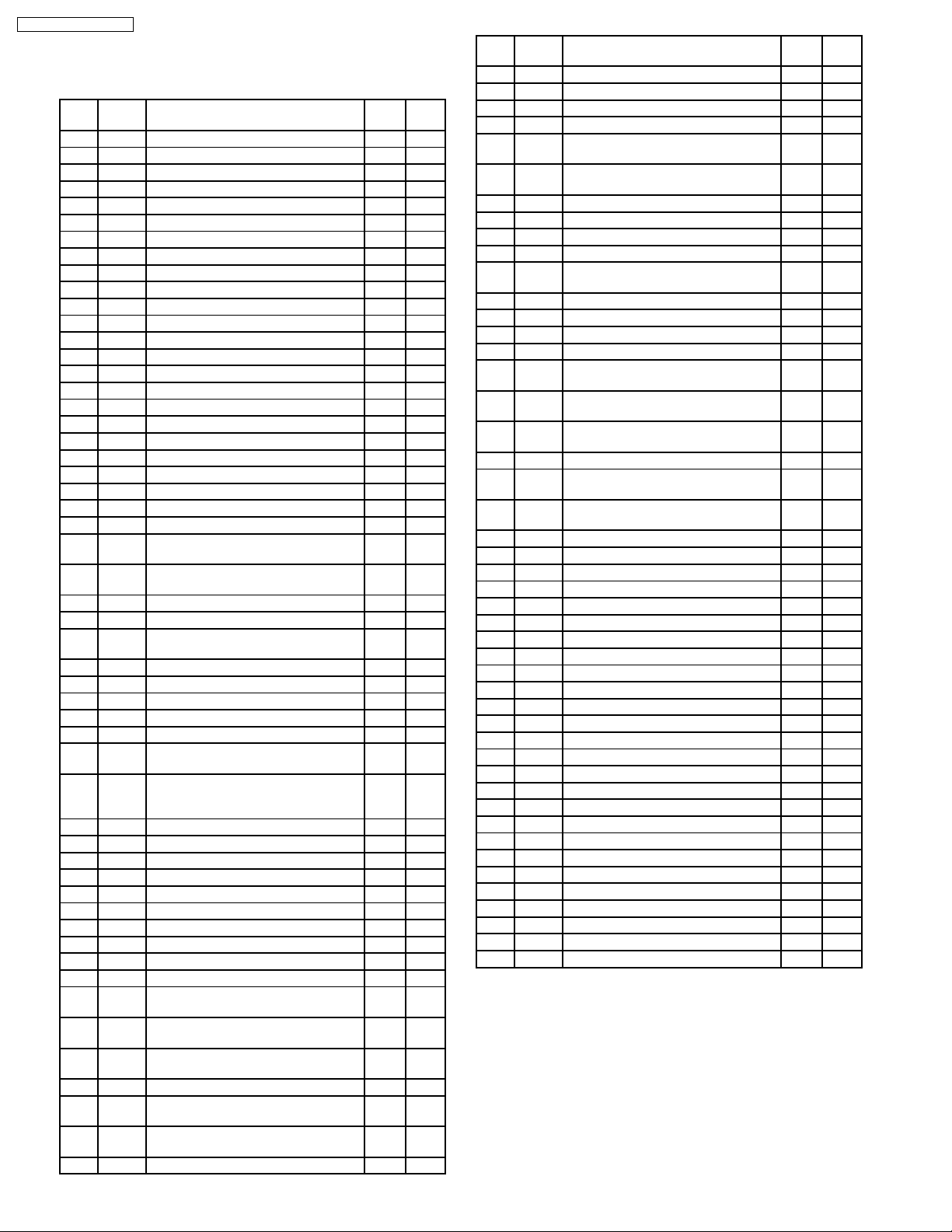
CQ-C7413U / CQ-C7113U
Ref. No. Part No. Part Name & Description Remarks
IC903 B3RAB0000054 Diode
CAPACITORs
C902 YECUZ1C104KX Ceramic, 0.1µF 16WV
C903 YECUZ1C104KX Ceramic, 0.1µF 16WV
C904 YECSW1C106MS Tantalum, 10µF 16WV
C907 YECUZ1C104KX Ceramic, 0.1µF 16WV
C908 YECUZ1C104KX Ceramic, 0.1µF 16WV
C911 YECUZ1C104KX Ceramic, 0.1µF 16WV
C912 YECSW1C106MS Tantalum, 10µF 16WV
C913 YECUZ1C104KX Ceramic, 0.1µF 16WV
C914 YECUS1C105ZF Ceramic, 1µF 16WV
C915 YECUS1C105ZF Ceramic, 1µF 16WV
C916 F1J1H102A672 Ceramic, 1000PF 50WV
C917 YECSW1C106MS Tantalum, 10µF 16WV
C918 YECSW1C106MS Tantalum, 10µF 16WV
C919 YECUZ1H103KX Ceramic, 0.01µF 50WV
C931 YECUV1C225KX Ceramic, 2.2µF 16WV
C932 YECUV1C225KX Ceramic, 2.2µF 16WV
C933 YECUV1C225KX Ceramic, 2.2µF 16WV
C934 YECUV1C225KX Ceramic, 2.2µF 16WV
C935 YECUV1C225KX Ceramic, 2.2µF 16WV
C936 YECUV1C225KX Ceramic, 2.2µF 16WV
C937 YECUV1C225KX Ceramic, 2.2µF 16WV
C938 YECUZ1C104KX Ceramic, 0.1µF 16WV
C939 YECUV1C225KX Ceramic, 2.2µF 16WV
C940 YECUV1C225KX Ceramic, 2.2µF 16WV
C941 YECUV1C225KX Ceramic, 2.2µF 16WV
C942 YECUV1C225KX Ceramic, 2.2µF 16WV
C973 YECUZ1H103KX Ceramic, 0.01µF 50WV
C974 YECUZ1H103KX Ceramic, 0.01µF 50WV
THERMISTORs
PT701 YERT7AR4R7MT Thermistor
[E9782] Display Block
IC´s AND TRANSISTORs
IC900 C2CBJH000133 IC
IC901 C3FBMD000236 IC
IC902 C0EBF0000374 IC
Q902 B1GDCFNN0002 Transistor
Q903 B1GBCFNN0004 Transistor
Q912 B1BBAC000014 Transistor
Q941 B1ABCF000187 Transistor
Q942 B1ABCF000187 Transistor
Q943 B1ABCF000187 Transistor
DIODEs
D901 B0BC5R600003 Diode
D903 B0BC4R000006 Diode
D906 B0BC01100039 Diode
D907 B3AFB0000091 Diode
D909 MA152WKTX Diode
D910 B0BC4R000006 Diode
D911 B0BC4R000006 Diode
D912 B0BC4R000006 Diode
D913 B0BC4R000006 Diode
D914 B0BC4R000006 Diode
D917 B0BC4R000006 Diode
D918 B0BC4R000006 Diode
D919 B0BC4R000006 Diode
D920 B0BC4R000006 Diode
D931 B3AZB0000031 Diode
D932 B3AZB0000031 Diode
D933 B3AZB0000031 Diode
D934 B3AZB0000031 Diode
D935 B3AZB0000031 Diode
D951 B3AFB0000091 Diode
D952 B3AFB0000091 Diode
D964 B0BC9R0A0058 Diode
RESISTORs
R902 ERJ3GEYJ103V Chip, 10kΩ 1/16W
R903 ERJ3GEYJ103V Chip, 10kΩ 1/16W
R904 ERJ3GEYJ103V Chip, 10kΩ 1/16W
R905 ERJ3GEYJ103V Chip, 10kΩ 1/16W
R911 ERJ3GEYJ222V Chip, 2.2kΩ 1/16W
R912 ERJ3GEYJ222V Chip, 2.2kΩ 1/16W
R913 ERJ3GEYJ222V Chip, 2.2kΩ 1/16W
R914 ERJ3GEYJ222V Chip, 2.2kΩ 1/16W
R916 ERJ3GEYJ184V Chip, 180kΩ 1/16W
R917 ERJ3GEYJ184V Chip, 180kΩ 1/16W
R918 ERJ3GEYJ184V Chip, 180kΩ 1/16W
R923 ERJ3GEYJ473V Chip, 47kΩ 1/16W
R924 ERJ3GEYJ104V Chip, 100kΩ 1/16W
R925 ERJ3GEYJ302V Chip, 3kΩ 1/16W
R928 ERJ3GEYJ222V Chip, 2.2kΩ 1/16W
R929 ERJ3GEYJ122V Chip, 1.2kΩ 1/16W
R932 ERJ3GEYJ101V Chip, 100Ω 1/16W
R933 ERJ6GEYJ751V Chip, 750Ω 1/10W
R934 ERJ3GEYJ103V Chip, 10kΩ 1/16W
R935 ERJ3GEYJ103V Chip, 10kΩ 1/16W
R936 ERJ3GEYJ103V Chip, 10kΩ 1/16W
R937 ERJ3GEYJ103V Chip, 10kΩ 1/16W
R941 ERJ8GEYJ471V Chip, 470Ω 1/8W
R942 ERJ8GEYJ331V Chip, 330Ω 1/8W
R943 ERJ8GEYJ391V Chip, 390Ω 1/8W
R944 ERJ8GEYJ471V Chip, 470Ω 1/8W
R945 ERJ8GEYJ331V Chip, 330Ω 1/8W
R946 ERJ8GEYJ391V Chip, 390Ω 1/8W
R947 ERJ3GEYJ562V Chip, 5.6kΩ 1/16W
R948 ERJ3GEYJ562V Chip, 5.6kΩ 1/16W
R949 ERJ3GEYJ562V Chip, 5.6kΩ 1/16W
R950 ERJ3GEYJ103V Chip, 10kΩ 1/16W
R952 ERJ3GEYJ473V Chip, 47kΩ 1/16W
R953 ERJ3GEYJ473V Chip, 47kΩ 1/16W
R954 ERJ3GEYJ473V Chip, 47kΩ 1/16W
R955 ERJ8GEYJ751V Chip, 750Ω 1/8W
R956 ERJ8GEYJ331V Chip, 330Ω 1/8W
R957 ERJ8GEYJ391V Chip, 390Ω 1/8W
R958 ERJ8GEYJ751V Chip, 750Ω 1/8W
21

CQ-C7413U / CQ-C7113U
Ref. No. Part No. Part Name & Description Remarks
R959 ERJ8GEYJ331V Chip, 330Ω 1/8W
R960 ERJ8GEYJ391V Chip, 390Ω 1/8W
R961 ERJ8GEYJ751V Chip, 750Ω 1/8W
R962 ERJ8GEYJ331V Chip, 330Ω 1/8W
R963 ERJ8GEYJ391V Chip, 390Ω 1/8W
R964 ERJ6GEYJ132V Chip, 1.3kΩ 1/10W
R969 ERJ3GEYJ473V Chip, 47kΩ 1/16W
R970 ERJ3GEYJ103V Chip, 10kΩ 1/16W
R971 ERJ3GEYJ103V Chip, 10kΩ 1/16W
R981 ERJ6GEYJ182 Chip, 1.8kΩ 1/10W
R982 ERJ6GEYJ102 Chip, 1kΩ 1/10W
TH900 ERJ3GEYJ473V Chip, 47kΩ 1/16W
CONNECTORs
CN901 K1NZ16D00001 Connector, 16P
CN902 K1MN30BA0109 Connector, 30P
CP904 YEAE0102ILA Connector, 2P
CP905 YEAE0102ILA Connector, 2P
SWITCHes
SW901 K9AA024A0013 Switch
SW902 K0H1BA000445 Switch
SW903 K0H1BA000445 Switch
SW905 K0H1BA000445 Switch
SW906 K0H1BA000445 Switch
SW907 K0H1BA000445 Switch
SW908 K0H1BA000445 Switch
SW909 K0H1BA000445 Switch
SW910 K0H1BA000445 Switch
SW911 K0H1BA000445 Switch
SW912 K0H1BA000445 Switch
SW913 K0H1BA000445 Switch
SW914 K0H1BA000445 Switch
CRYSTALs
XL900 H2C122500003 Ceramic Oscillator
LCD
LCD901 L5F000000010 LCD
Accessories
PRINTINGs
INSTALLATION PARTS
EUR7641010 Remote Control Unit (includes a
CR2025/1F Lithium Battery
YGAJ021009 Power Connector
YEFX0217222 Mounting Collar
YEFC051013 Trim Plate
YEP0FZ5701 Installation Kit (Lock Cancel Plate,
YEFG04019 Rear Support Strap
YEFA134150 Removable Face Plate Case
YEP0FZ5702 Security Screw Kit
- Operating Instructions TSN
- System Upgrade Guidebook TSN
- Installation Instructions TSN
battery)
Mounting Bolt, Tapping Screw, Hex
Nut)
Ref. No. Part No. Part Name & Description Remarks
AP2 YGAP2985 FPC
AT1-3 K4ZZ01000048 Terminal
CN1 K1NZ16H00002 Connector, 16P
HP1 YEAT03324 Terminal
HP2 K4ZZ01000044 Terminal
1 YEFA031898A Upper Cover
2 YEP0FX13468 Removable Face Plate Unit RTL
3 YEFA134121 Back Cover, Detachable
4 YEFX9995929 Optical Shade
5 YGP0PT9782V9 Display PCB w/Component RTL
8 YEFX0013087 Prism Mirror
9 YEFX9995567 Reflection Sheet
10 YEFK061408 LCD Holder
11 YEFX0052572 Spring, Knob Vol
12 YEFE071005 Knob, Vol
13 YEFV023487 Diffusion Sheet, LCD901
14 YEFX0217430 Case, LCD901
15 YEFX9995490 Spacer
16 YESFC02229 Detachable Face Ass´y
17 YEFE1310578 Button, TUNE/TRACK Base
18 YEFJ013161 Vol Plate B
19 YEFE1310577 Button, TUNE/TRACK Cap
21 YEFK061410 Shading Cover
22 YEFV023497 Optical Shade
23 YEFX0013229 Transparent Plate
24 YEFV023498 Optical Shade
25 YEFE1310573 Button, SRC
26 YEFE1310574 Button, MENU, BAND, D
27 YEFE1310723 Button, EJ/D-M/SQ/MUTE
28 YEFE1310579 Button, RELEASE
29 YEFX0053029 Spring, RELEASE
35 YEFR041000 Cap
36 YEFM031549 Laser Seal
40 YEFA07669 Front Plate
41 YEFC028113 Rear Cover, Escutcheon
42 YEFS02431 Pad
43 YEFX0012368 Transparent Plate, Escutcheon
44 YEFS012112 Pad, Escutcheon
45 YEFC028112 Front Cover, Escutcheon
46 YEFA131827 Flexible PCB Case
47 YEP9FX352 Drive, Mechanical Assy
48 YGP0PT3108Q9 Main/Sub PCB W/Component RTL
49 YEFX0216269 Bracket, IC730
50 YEFX0213945B Bracket, IC271
51 YEFF011230 Heat Sink
52 YEFX007685 Clamper
53 YEFA081009 Rear Plate
54 YEFV012641 Insulator
55 YEFX0217229 Bracket, IC701
56 YEFV034018 Magnetic Shield
70 YEJS06404A Binding Screw
71 XTB2+6GFJ Tapping Screw
73 YEJT03333A Tapping Screw
74 XQN2+C4FJK Machin Screw
75 XQN2+BG8FJK Machin Screw
76 XSB3+14FJ Binding Screw
77 XSB3+6FJ Binding Screw
78 XSB26+5FJ Binding Screw
80 XTB3+6FFJ Tapping Screw
81 XTB26+6FFJ Tapping Screw
Mechanical Parts
MISCELLANEOUS
ANT51 YEAA10090 Antenna Receptacle
22
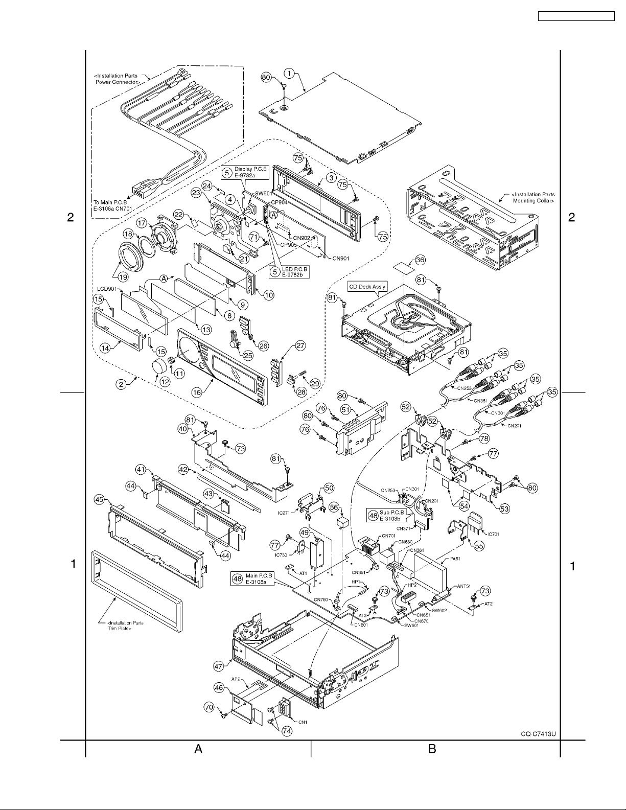
14 EXPLODED VIEW (Unit) [CQ-C7413U]
CQ-C7413U / CQ-C7113U
23

CQ-C7413U / CQ-C7113U
15 REPLACEMENT PARTS
LIST [CQ-C7113U]
Notes :
1. Be sure to make your orders of replacement parts
according to this list.
2. Important safety notice: Components, identified by
have special characteristics important for safety. When
replacing any of these components, use only
manufacturer´s specified parts.
3. Location keys in the remarks column indicates the general
location of the parts shown in the exploded drawing, as in a
road map.
4. The marking (RTL) indicates that Retention Time is limited
for this item. After the discontinuation of assembly in
production, the item will continue to be available for a
specific period of time. The retention period of availability is
dependent on the type of assembly, and in accordance with
the laws governing part and product retention. After the end
of this period, the assembly will no longer be available.
· Order intake period is basically six months after the first
shipment.
5. Reference materials of parts with the “TSN“ mark in the
remarks column are uploaded in the TSN (Technical
Service Navigation) system website. Please download from
that website for references.
Ref. No. Part No. Part Name & Description Remarks
[E3109] Main Block
IC´s AND TRANSISTORs
IC201 C1BB00001132 IC
IC271 C1ZAZ0001450 IC
IC401 C1BB00001045 IC
IC601 C2CBKG000035 IC
IC630 C0JBAA000372 IC
IC650 C0JBAA000372 IC
IC670 YEAMC14584BE IC
IC701 C0DAZHF00004 IC
IC702 C0EBZ0000035 IC
IC720 C0CBCYG00004 IC
IC730 C0DAEKG00002 IC
IC752 C0CAABG00012 IC
IC755 C0DBZGD00040 IC
IC760 C0GBG0000032 IC
PA51 C5BA00000122 Electronic Tuner
Q55 B1GDGFEH0001 Transistor
Q56 B1AAEC000002 Transistor
Q220 B1GBCFNN0004 Transistor
Q262 B1GBHBEA0004 Transistor
Q266 B1GBHBEA0004 Transistor
Q320 B1GBCFNN0004 Transistor
Q346 B1GBHBEA0004 Transistor
Q362 B1GBHBEA0004 Transistor
Q366 B1GBHBEA0004 Transistor
Q372 YEANC114YKX Transistor
Q376 B1GBCFNN0004 Transistor
Q411 B1CBGF000005 Transistor
Q630 B1GBCFNN0004 Transistor
Q633 B1GDCFJJ0002 Transistor
Q650 YEANC114YKX Transistor
Q651 B1GBCFNN0004 Transistor
Q652 B1GBCFNN0004 Transistor
Q680 B1GDGFEH0001 Transistor
Q681 B1GDCFJJ0002 Transistor
Q701 B1BACF000026 Transistor
Q760 B1GBCFNN0004 Transistor
Q791 B1GBNCEJ0003 Transistor
mark
Ref. No. Part No. Part Name & Description Remarks
Q793 YEANC114YKX Transistor
DIODEs
D201 B0JCME000012 Diode
D202 B0JCME000012 Diode
D203 B0JCME000012 Diode
D204 B0JCME000012 Diode
D301 B0JCME000012 Diode
D302 B0JCME000012 Diode
D303 B0JCME000012 Diode
D304 B0JCME000012 Diode
D346 B0JCMC000004 Diode
D601 B0JCMC000004 Diode
D630 B3AAB0000143 Diode
D631 B0BC5R600003 Diode
D632 B0BC5R600003 Diode
D633 MA3X152A0L Diode
D635 B0BC5R600003 Diode
D636 B0BC5R600003 Diode
D638 B0BC5R600003 Diode
D639 B0BC5R600003 Diode
D670 B0JCMC000004 Diode
D672 B0JCMC000004 Diode
D673 B0BC5R000020 Diode
D701 YEADDAM3MA47 Diode
D702 MA736TX Diode
D703 B0BC5R7A0062 Diode
D704 B0JCMC000004 Diode
D705 YEADSR1544TL Diode
D706 YEADSR1544TL Diode
D707 YEADRB051L40 Diode
D708 MA736TX Diode
D710 B0JCMC000004 Diode
D715 MA3X152A0L Diode
D716 MA721TX Diode
D760 B0BC5R000020 Diode
D761 B0BC3R0A0058 Diode
CAPACITORs
C52 YECUS1H470JC Ceramic, 47PF 50WV
C53 F1J1H103A513 Ceramic, 0.01µF 50WV
C54 F2A1A221A449 Electrolytic, 220µF 10WV
C55 F1J1H103A513 Ceramic, 0.01µF 50WV
C56 F3F1E105A001 Tantalum, 1µF 25WV
C57 F2A1A101A450 Electrolytic, 100µF 10WV
C61 YECUS1E273KX Ceramic, 0.027µF 25WV
C62 YECUS1E273KX Ceramic, 0.027µF 25WV
C65 F1J1H1020024 Ceramic, 1000PF 50WV
C206 YECUV1A225KX Ceramic, 2.2µF 10WV
C213 F1J1A2250004 Ceramic, 2.2µF 10WV
C215 F1J1A2250004 Ceramic, 2.2µF 10WV
C217 YECUS1C334KX Ceramic, 0.33µF 16WV
C220 F2A1H2R2A634 Electrolytic, 2.2µF 50WV
C250 YECUS1C224KX Ceramic, 0.22µF 16WV
C261 F2A1H4R7A632 Electrolytic, 4.7µF 50WV
C263 ECQV1H474JL2 Plastic Film, 0.47µF 50WV
C265 F2A1H4R7A632 Electrolytic, 4.7µF 50WV
C267 ECQV1H474JL2 Plastic Film, 0.47µF 50WV
C271 F1J1H472A675 Ceramic, 4700PF 50WV
C272 F1J1H472A675 Ceramic, 4700PF 50WV
C274 F2A1C470A630 Electrolytic, 47µF 16WV
C275 F1J1C1050013 Ceramic, 1µF 16WV
C278 YECUS1E104ZF Ceramic, 0.1µF 25WV
C279 F2A1C2220069 Electrolytic, 2200µF 16WV
C306 YECUV1A225KX Ceramic, 2.2µF 10WV
C313 F1J1A2250004 Ceramic, 2.2µF 10WV
C314 F1L1C1060018 Ceramic, 10µF 16WV
C315 F1J1A2250004 Ceramic, 2.2µF 10WV
C317 YECUS1C334KX Ceramic, 0.33µF 16WV
C320 F2A1H2R2A634 Electrolytic, 2.2µF 50WV
C323 YECUV1A225KX Ceramic, 2.2µF 10WV
C327 F2A1A221A449 Electrolytic, 220µF 10WV
24

Ref. No. Part No. Part Name & Description Remarks
C328 F1J1H103A513 Ceramic, 0.01µF 50WV
C345 F2A1C100A502 Electrolytic, 10µF 16WV
C361 F2A1H4R7A632 Electrolytic, 4.7µF 50WV
C363 ECQV1H474JL2 Plastic Film, 0.47µF 50WV
C365 F2A1H4R7A632 Electrolytic, 4.7µF 50WV
C367 ECQV1H474JL2 Plastic Film, 0.47µF 50WV
C371 F1J1H472A675 Ceramic, 4700PF 50WV
C372 F1J1H472A675 Ceramic, 4700PF 50WV
C374 F2A1H2R2A634 Electrolytic, 2.2µF 50WV
C375 F2A1C100A502 Electrolytic, 10µF 16WV
C378 YECUS1E104ZF Ceramic, 0.1µF 25WV
C401 F1J1H120A034 Ceramic, 12PF 50WV
C402 F1J1H120A034 Ceramic, 12PF 50WV
C403 F2A0J101A500 Electrolytic, 100µF 6.3WV
C404 F1J1H103A513 Ceramic, 0.01µF 50WV
C405 F1H1H101A231 Ceramic, 100PF 50WV
C411 F1J1H103A513 Ceramic, 0.01µF 50WV
C412 YECUS1E223KX Ceramic, 0.022µF 25WV
C413 ECQV1H224JL2 Plastic Film, 0.22µF 50WV
C414 F2A1A221A449 Electrolytic, 220µF 10WV
C601 YECUZ1C104KX Ceramic, 0.1µF 16WV
C602 YECUZ1H103KX Ceramic, 0.01µF 50WV
C603 F2A0J3310051 Electrolytic, 330µF 6.3WV
C605 YECUZ1C104KX Ceramic, 0.1µF 16WV
C606 F1H1H2200008 Ceramic, 22PF 50WV
C607 F1H1H2200008 Ceramic, 22PF 50WV
C608 YECUS1C104KX Ceramic, 0.1µF 16WV
C609 F1J1A106A023 Ceramic, 10µF 10WV
C610 YECUS1C104KX Ceramic, 0.1µF 16WV
C616 F1H1H120A231 Ceramic, 12PF 50WV
C617 F1H1H120A231 Ceramic, 12PF 50WV
C631 F2A1H4R7A632 Electrolytic, 4.7µF 50WV
C632 YECUS1E104ZF Ceramic, 0.1µF 25WV
C633 F2A1C470A630 Electrolytic, 47µF 16WV
C634 YECUZ1H103KX Ceramic, 0.01µF 50WV
C635 F1J1H103A513 Ceramic, 0.01µF 50WV
C650 F1J1H103A513 Ceramic, 0.01µF 50WV
C651 YECUS1C224ZF Ceramic, 0.22µF 16WV
C652 YECUS1C224ZF Ceramic, 0.22µF 16WV
C670 F2A1C100A502 Electrolytic, 10µF 16WV
C671 YECUZ1H103KX Ceramic, 0.01µF 50WV
C680 F2A1H2R2A634 Electrolytic, 2.2µF 50WV
C701 F1H1A154A007 Ceramic, 0.15µF 10WV
C702 F2A1C1020069 Electrolytic, 1000µF 16WV
C704 F2A0J470A558 Electrolytic, 47µF 6.3WV
C705 YECUZ1H103KX Ceramic, 0.01µF 50WV
C706 ECA0JM102 Electrolytic, 1000µF 6.3WV
C707 F2A1C1020069 Electrolytic, 1000µF 16WV
C708 F2A1H1R00095 Electrolytic, 1µF 50WV
C713 YECUS1C474KX Ceramic, 0.47µF 16WV
C715 YECUS1E104ZF Ceramic, 0.1µF 25WV
C716 YECUS1C104KX Ceramic, 0.1µF 16WV
C717 YECUS1C104KX Ceramic, 0.1µF 16WV
C718 YECUS1E104ZF Ceramic, 0.1µF 25WV
C719 EEAFC1A820H Electrolytic, 82µF 10WV
C720 YECUS1C104KX Ceramic, 0.1µF 16WV
C721 YECUS1C104KX Ceramic, 0.1µF 16WV
C727 F1K1E334A022 Ceramic, 0.33µF 25WV
C728 YECUS1C334KX Ceramic, 0.33µF 16WV
C729 EEAFC1C560H Electrolytic, 56µF 16WV
C730 F1K1E334A022 Ceramic, 0.33µF 25WV
C731 YECUX1C334KX Ceramic, 0.33µF 16WV
C732 EEAFC1C560H Electrolytic, 56µF 16WV
C752 YECUS1C104KX Ceramic, 0.1µF 16WV
C753 YECUS1C104KX Ceramic, 0.1µF 16WV
C754 EEAFC0J560H Electrolytic, 56µF 6.3WV
C755 YECUZ1C104KX Ceramic, 0.1µF 16WV
C756 F1J1C1050013 Ceramic, 1µF 16WV
C757 YECUZ1H103KX Ceramic, 0.01µF 50WV
C758 F2A0J470A558 Electrolytic, 47µF 6.3WV
C760 YECUZ1H103KX Ceramic, 0.01µF 50WV
C761 YECUS1E104ZF Ceramic, 0.1µF 25WV
C762 F2A1C470A630 Electrolytic, 47µF 16WV
C763 YECUS1E104ZF Ceramic, 0.1µF 25WV
CQ-C7413U / CQ-C7113U
Ref. No. Part No. Part Name & Description Remarks
C797 YECUS1E104ZF Ceramic, 0.1µF 25WV
RESISTORs
J401 ERJ8GEY0R00V Chip, 0Ω 1/8W
J403 ERJ6GEY0R00V Chip, 0Ω 1/10W
J404 ERJ6GEY0R00V Chip, 0Ω 1/10W
J409 ERJ6GEY0R00V Chip, 0Ω 1/10W
J410 ERJ6GEY0R00V Chip, 0Ω 1/10W
J501 ERJ8GEY0R00V Chip, 0Ω 1/8W
J502 ERJ8GEY0R00V Chip, 0Ω 1/8W
J504 ERJ6GEY0R00V Chip, 0Ω 1/10W
J506 ERJ8GEY0R00V Chip, 0Ω 1/8W
J507 ERJ8GEY0R00V Chip, 0Ω 1/8W
J510 ERJ8GEY0R00V Chip, 0Ω 1/8W
J513 ERJ8GEY0R00V Chip, 0Ω 1/8W
J514 ERJ8GEY0R00V Chip, 0Ω 1/8W
J515 ERJ8GEY0R00V Chip, 0Ω 1/8W
J517 ERJ8GEY0R00V Chip, 0Ω 1/8W
J518 ERJ8GEY0R00V Chip, 0Ω 1/8W
J520 ERJ8GX0R00V Chip, 0Ω 1/8W
J521 ERJ8GX0R00V Chip, 0Ω 1/8W
J522 ERJ8GX0R00V Chip, 0Ω 1/8W
J523 ERJ8GX0R00V Chip, 0Ω 1/8W
J524 ERJ8GX0R00V Chip, 0Ω 1/8W
J525 ERJ8GX0R00V Chip, 0Ω 1/8W
J526 ERJ8GX0R00V Chip, 0Ω 1/8W
J527 ERJ8GX0R00V Chip, 0Ω 1/8W
J529 ERJ8GX0R00V Chip, 0Ω 1/8W
J531 ERJ8GX0R00V Chip, 0Ω 1/8W
J532 ERJ8GX0R00V Chip, 0Ω 1/8W
J533 ERJ8GX0R00V Chip, 0Ω 1/8W
J534 ERJ8GX0R00V Chip, 0Ω 1/8W
J536 ERJ8GX0R00V Chip, 0Ω 1/8W
J537 ERJ8GX0R00V Chip, 0Ω 1/8W
J538 ERJ8GX0R00V Chip, 0Ω 1/8W
J539 ERJ8GX0R00V Chip, 0Ω 1/8W
J540 ERJ8GX0R00V Chip, 0Ω 1/8W
J541 ERJ8GEY0R00V Chip, 0Ω 1/8W
J542 ERJ8GX0R00V Chip, 0Ω 1/8W
J544 ERJ8GX0R00V Chip, 0Ω 1/8W
J545 ERJ8GX0R00V Chip, 0Ω 1/8W
J546 ERJ8GX0R00V Chip, 0Ω 1/8W
J550 ERJ8GX0R00V Chip, 0Ω 1/8W
J551 ERJ8GX0R00V Chip, 0Ω 1/8W
J553 ERJ8GX0R00V Chip, 0Ω 1/8W
J554 ERJ8GX0R00V Chip, 0Ω 1/8W
J555 ERJ6GEY0R00V Chip, 0Ω 1/10W
J558 ERJ6GEY0R00V Chip, 0Ω 1/10W
J560 ERJ8GEY0R00V Chip, 0Ω 1/8W
J561 ERJ8GEY0R00V Chip, 0Ω 1/8W
J562 ERJ6GEY0R00V Chip, 0Ω 1/10W
J563 ERJ8GX0R00V Chip, 0Ω 1/8W
J564 ERJ8GEY0R00V Chip, 0Ω 1/8W
J565 ERJ8GX0R00V Chip, 0Ω 1/8W
J566 ERJ8GEY0R00V Chip, 0Ω 1/8W
J568 ERJ8GX0R00V Chip, 0Ω 1/8W
J570 ERJ8GEY0R00V Chip, 0Ω 1/8W
J571 ERJ8GEY0R00V Chip, 0Ω 1/8W
J572 ERJ8GEY0R00V Chip, 0Ω 1/8W
J578 ERJ6GEY0R00V Chip, 0Ω 1/10W
J579 ERJ8GEY0R00V Chip, 0Ω 1/8W
J580 ERJ8GX0R00V Chip, 0Ω 1/8W
J582 ERJ8GEY0R00V Chip, 0Ω 1/8W
J583 ERJ8GEY0R00V Chip, 0Ω 1/8W
J584 ERJ6GEY0R00V Chip, 0Ω 1/10W
J585 ERJ6GEY0R00V Chip, 0Ω 1/10W
J589 ERJ8GEY0R00V Chip, 0Ω 1/8W
J590 ERJ8GEY0R00V Chip, 0Ω 1/8W
J591 ERJ6GEY0R00V Chip, 0Ω 1/10W
J593 ERJ8GX0R00V Chip, 0Ω 1/8W
J594 ERJ8GX0R00V Chip, 0Ω 1/8W
J595 ERJ6GEY0R00V Chip, 0Ω 1/10W
J596 ERJ8GX0R00V Chip, 0Ω 1/8W
25

CQ-C7413U / CQ-C7113U
Ref. No. Part No. Part Name & Description Remarks
J597 ERJ8GEY0R00V Chip, 0Ω 1/8W
J599 ERJ8GX0R00V Chip, 0Ω 1/8W
J794 ERJ8GX0R00V Chip, 0Ω 1/8W
L53 ERJ8GEY0R00V Chip, 0Ω 1/8W
L295 ERD6GEYJ180 Chip, 18Ω 1/10W
L296 ERD6GEYJ180 Chip, 18Ω 1/10W
L395 ERD6GEYJ180 Chip, 18Ω 1/10W
L396 ERD6GEYJ180 Chip, 18Ω 1/10W
R50 ERJ6GEYJ5R6V Chip, 5.6Ω 1/10W
R51 ERJ6GEY0R00V Chip, 0Ω 1/10W
R54 ERJ6GEYJ101 Chip, 100Ω 1/10W
R55 ERJ6GEYJ221 Chip, 220Ω 1/10W
R56 ERJ6GEYJ102 Chip, 1kΩ 1/10W
R59 ERJ3GEYJ104V Chip, 100kΩ 1/16W
R65 ERJ6GEYJ393 Chip, 39kΩ 1/10W
R202 ERJ6GEYJ152 Chip, 1.5kΩ 1/10W
R203 ERJ6GEYJ103 Chip, 10kΩ 1/10W
R209 ERJ6GEYJ102 Chip, 1kΩ 1/10W
R213 ERJ6GEYJ562 Chip, 5.6kΩ 1/10W
R214 ERJ3GEYJ103V Chip, 10kΩ 1/16W
R215 ERJ3GEYJ472V Chip, 4.7kΩ 1/16W
R216 ERJ3GEYJ123V Chip, 12kΩ 1/16W
R217 ERJ3GEYJ183V Chip, 18kΩ 1/16W
R220 ERJ6GEYJ750V Chip, 75Ω 1/10W
R221 ERJ6GEYJ563 Chip, 56kΩ 1/10W
R247 ERJ8GEY0R00V Chip, 0Ω 1/8W
R248 ERD6GEYJ180 Chip, 18Ω 1/10W
R250 ERJ6GEYJ102 Chip, 1kΩ 1/10W
R251 ERJ6GEY0R00V Chip, 0Ω 1/10W
R257 ERJ6GEY0R00V Chip, 0Ω 1/10W
R261 ERJ6GEYJ181 Chip, 180Ω 1/10W
R262 ERJ3GEYJ103V Chip, 10kΩ 1/16W
R263 ERJ6GEYJ561 Chip, 560Ω 1/10W
R265 ERJ6GEYJ181 Chip, 180Ω 1/10W
R266 ERJ3GEYJ103V Chip, 10kΩ 1/16W
R267 ERJ8GEYJ561V Chip, 560Ω 1/8W
R275 ERJ8GEYJ223V Chip, 22kΩ 1/8W
R302 ERJ6GEYJ152 Chip, 1.5kΩ 1/10W
R303 ERJ6GEYJ103 Chip, 10kΩ 1/10W
R313 ERJ6GEYJ562 Chip, 5.6kΩ 1/10W
R314 ERJ3GEYJ103V Chip, 10kΩ 1/16W
R315 ERJ3GEYJ472V Chip, 4.7kΩ 1/16W
R316 ERJ3GEYJ123V Chip, 12kΩ 1/16W
R317 ERJ3GEYJ183V Chip, 18kΩ 1/16W
R320 ERJ6GEYJ750V Chip, 75Ω 1/10W
R321 ERJ6GEYJ563 Chip, 56kΩ 1/10W
R323 ERJ3GEYJ102V Chip, 1kΩ 1/16W
R324 ERJ6GEYJ103 Chip, 10kΩ 1/10W
R325 ERJ6GEYJ102 Chip, 1kΩ 1/10W
R326 ERJ6GEYJ101 Chip, 100Ω 1/10W
R327 ERJ6GEYJ823 Chip, 82kΩ 1/10W
R345 ERJ6GEYJ181 Chip, 180Ω 1/10W
R346 ERJ3GEYJ223V Chip, 22kΩ 1/16W
R348 ERD6GEYJ180 Chip, 18Ω 1/10W
R351 ERJ8GEY0R00V Chip, 0Ω 1/8W
R357 ERJ6GEY0R00V Chip, 0Ω 1/10W
R361 ERJ6GEYJ181 Chip, 180Ω 1/10W
R362 ERJ3GEYJ103V Chip, 10kΩ 1/16W
R363 ERJ6GEYJ561 Chip, 560Ω 1/10W
R365 ERJ6GEYJ181 Chip, 180Ω 1/10W
R366 ERJ3GEYJ103V Chip, 10kΩ 1/16W
R367 ERJ6GEYJ561 Chip, 560Ω 1/10W
R373 ERJ3GEYJ183V Chip, 18kΩ 1/16W
R375 ERJ6GEYJ562 Chip, 5.6kΩ 1/10W
R376 ERJ3GEYJ103V Chip, 10kΩ 1/16W
R401 ERJ3GEYJ152V Chip, 1.5kΩ 1/16W
R402 ERJ3GEYJ472V Chip, 4.7kΩ 1/16W
R403 ERJ3GEYJ473V Chip, 47kΩ 1/16W
R404 ERJ3GEYJ102V Chip, 1kΩ 1/16W
R405 ERJ3GEYJ102V Chip, 1kΩ 1/16W
R406 ERJ3GEYJ102V Chip, 1kΩ 1/16W
R407 ERJ3GEYJ102V Chip, 1kΩ 1/16W
R408 ERJ3GEYJ473V Chip, 47kΩ 1/16W
R409 ERJ3GEYJ102V Chip, 1kΩ 1/16W
Ref. No. Part No. Part Name & Description Remarks
R410 ERJ3GEY0R00V Chip, 0Ω 1/16W
R411 ERJ3GEYJ221V Chip, 220Ω 1/16W
R413 ERJ6GEYJ182 Chip, 1.8kΩ 1/10W
R414 ERJ8GEYJ561V Chip, 560Ω 1/8W
R417 ERJ3GEYJ100V Chip, 10Ω 1/16W
R601 ERJ3GEYJ432V Chip, 4.3kΩ 1/16W
R602 ERJ3GEYJ432V Chip, 4.3kΩ 1/16W
R605 ERJ3GEYJ102V Chip, 1kΩ 1/16W
R607 ERJ3GEYJ333V Chip, 33kΩ 1/16W
R608 ERJ3GEYJ822V Chip, 8.2kΩ 1/16W
R610 ERJ3GEYJ473V Chip, 47kΩ 1/16W
R611 ERJ3GEYJ683V Chip, 68kΩ 1/16W
R612 ERJ3GEYJ153V Chip, 15kΩ 1/16W
R613 ERJ3GEYJ103V Chip, 10kΩ 1/16W
R614 ERJ3GEYJ103V Chip, 10kΩ 1/16W
R615 ERJ6GEYJ103 Chip, 10kΩ 1/10W
R617 ERJ3GEYJ103V Chip, 10kΩ 1/16W
R618 ERJ3GEYJ223V Chip, 22kΩ 1/16W
R619 ERJ3GEYJ104V Chip, 100kΩ 1/16W
R620 ERJ3GEYJ103V Chip, 10kΩ 1/16W
R621 ERJ3GEYJ472V Chip, 4.7kΩ 1/16W
R622 ERJ6GEYJ473 Chip, 47kΩ 1/10W
R625 ERJ3GEYJ473V Chip, 47kΩ 1/16W
R626 ERJ6GEYJ102 Chip, 1kΩ 1/10W
R627 ERJ3GEYJ103V Chip, 10kΩ 1/16W
R628 ERJ3GEYJ103V Chip, 10kΩ 1/16W
R631 ERJ6GEYJ821 Chip, 820Ω 1/10W
R632 ERJ3GEYJ684V Chip, 680kΩ 1/16W
R634 ERJ6GEYJ561 Chip, 560Ω 1/10W
R636 ERJ6GEYJ473 Chip, 47kΩ 1/10W
R638 ERJ3GEYJ102V Chip, 1kΩ 1/16W
R639 ERJ3GEYJ102V Chip, 1kΩ 1/16W
R640 ERJ6GEYJ561 Chip, 560Ω 1/10W
R642 ERJ6GEYJ102 Chip, 1kΩ 1/10W
R645 ERJ3GEYJ561V Chip, 560Ω 1/16W
R646 ERJ3GEYJ104V Chip, 100kΩ 1/16W
R649 ERJ3GEYJ473V Chip, 47kΩ 1/16W
R653 ERJ3GEYJ512V Chip, 5.1kΩ 1/16W
R654 ERJ6GEYJ512V Chip, 5.1kΩ 1/10W
R655 ERJ6GEYJ103 Chip, 10kΩ 1/10W
R656 ERJ6GEYJ272 Chip, 2.7kΩ 1/10W
R657 ERJ3GEYJ272V Chip, 2.7kΩ 1/16W
R658 ERJ6GEYJ473 Chip, 47kΩ 1/10W
R659 ERJ6GEYJ272 Chip, 2.7kΩ 1/10W
R660 ERJ6GEYJ272 Chip, 2.7kΩ 1/10W
R661 ERJ3GEYJ473V Chip, 47kΩ 1/16W
R662 ERJ6GEYJ472 Chip, 4.7kΩ 1/10W
R663 ERJ6GEYJ512V Chip, 5.1kΩ 1/10W
R664 ERJ6GEYJ512V Chip, 5.1kΩ 1/10W
R666 ERJ3GEYJ561V Chip, 560Ω 1/16W
R670 ERJ6GEYJ104 Chip, 100kΩ 1/10W
R671 ERJ6GEYJ104 Chip, 100kΩ 1/10W
R672 ERJ6GEYJ104 Chip, 100kΩ 1/10W
R673 ERJ6GEYJ104 Chip, 100kΩ 1/10W
R674 ERJ3GEYJ272V Chip, 2.7kΩ 1/16W
R675 ERJ6GEYJ272 Chip, 2.7kΩ 1/10W
R676 ERJ6GEYJ472 Chip, 4.7kΩ 1/10W
R677 ERJ6GEYJ561 Chip, 560Ω 1/10W
R679 ERJ6GEYJ473 Chip, 47kΩ 1/10W
R680 ERJ6GEYJ561 Chip, 560Ω 1/10W
R681 ERJ6GEYJ562 Chip, 5.6kΩ 1/10W
R684 ERJ3GEYJ561V Chip, 560Ω 1/16W
R685 ERJ6GEYJ561 Chip, 560Ω 1/10W
R686 ERJ3GEYJ561V Chip, 560Ω 1/16W
R688 ERJ3GEYJ473V Chip, 47kΩ 1/16W
R689 ERJ3GEYJ473V Chip, 47kΩ 1/16W
R690 ERJ6GEYJ561 Chip, 560Ω 1/10W
R691 ERJ6GEYJ561 Chip, 560Ω 1/10W
R701 ERJ3GEYJ104V Chip, 100kΩ 1/16W
R702 ERJ3GEYJ224V Chip, 220kΩ 1/16W
R703 ERJ3GEYJ473V Chip, 47kΩ 1/16W
R704 ERJ8GEYJ4R7V Chip, 4.7Ω 1/8W
R705 ERJ8GEYJ682V Chip, 6.8kΩ 1/8W
R706 ERJ6GEYJ684 Chip, 680kΩ 1/10W
26

Ref. No. Part No. Part Name & Description Remarks
R715 ERJ3GEYJ472V Chip, 4.7kΩ 1/16W
R716 ERJ6GEYJ473 Chip, 47kΩ 1/10W
R717 ERJ3GEYJ433V Chip, 43kΩ 1/16W
R727 ERJ6ENF1002 Chip, 10kΩ 1/10W
R728 ERJ6ENF2703V Chip, 270kΩ 1/10W
R729 ERJ6ENF2001V Chip, 2kΩ 1/10W
R732 ERJ6ENF1802V Chip, 18kΩ 1/10W
R733 ERJ6ENF1303V Chip, 130kΩ 1/10W
R734 ERJ6ENF2201V Chip, 2.2kΩ 1/10W
R755 ERJ6GEYJ102 Chip, 1kΩ 1/10W
R760 ERJ6GEYJ152 Chip, 1.5kΩ 1/10W
R761 ERDS1FJ3R9 Carbon, 3.9Ω 1/2W
R770 ERJ6GEY0R00V Chip, 0Ω 1/10W
R790 ERJ3GEYJ223V Chip, 22kΩ 1/16W
R791 ERJ6GEYJ223 Chip, 22kΩ 1/10W
CONNECTORs
CN201 K2KF29Z00038 Plug, 4P
CN253 K2KF29Z00035 Plug, 4P
CN301 K2KF29Z00037 Plug, 4P
CN351 K2KF29Z00033 Plug, 4P
CN600 K1KB08A00068 Connector, 8P
CN601 K1MN16BA0111 Connector, 16P
CN651 K1KA18A00074 Connector, 18P
CN670 K1PQ07A00005 Connector, 7P
CN680 K1AA113B0002 Connector, 13P
CN701 K1FA116B0028 Connector, 16P
CN760 YEAE5339802 Connector, 2P
CQ-C7413U / CQ-C7113U
Ref. No. Part No. Part Name & Description Remarks
Q912 B1BBAC000014 Transistor
Q941 B1ABCF000187 Transistor
Q942 B1ABCF000187 Transistor
Q943 B1ABCF000187 Transistor
DIODEs
D901 B0BC5R600003 Diode
D903 B0BC4R000006 Diode
D906 B0BC01100039 Diode
D907 B3AFB0000091 Diode
D909 MA152WKTX Diode
D910 B0BC4R000006 Diode
D911 B0BC4R000006 Diode
D912 B0BC4R000006 Diode
D913 B0BC4R000006 Diode
D914 B0BC4R000006 Diode
D917 B0BC4R000006 Diode
D918 B0BC4R000006 Diode
D919 B0BC4R000006 Diode
D920 B0BC4R000006 Diode
D931 B3AZB0000031 Diode
D932 B3AZB0000031 Diode
D933 B3AZB0000031 Diode
D934 B3AZB0000031 Diode
D935 B3AZB0000031 Diode
D951 B3AFB0000091 Diode
D952 B3AFB0000091 Diode
D964 B0BC9R0A0058 Diode
IC903 B3RAB0000054 Diode
COILs
L50 G1C150K00011 Coil
L52 G1CR56JA0036 Coil
L401 G1C101JA0036 Coil
L601 G1C330JA0036 Coil
L602 G1C101JA0036 Coil
L603 G1C330JA0036 Coil
L630 G0C330K00004 RF Coil
L701 YELTBL01R1AT Coil
L702 G0A151J00006 Coil
SWITCHes
SW601 K0L1BA000099 Switch
SW602 K0L1BA000104 Switch
CRYSTALs
XL401 H0D720400006 Crystal Oscillator
XL601 H0D368400015 Crystal Oscillator
XL602 H0J327200161 Crystal Oscillator
NETWORK RESISTORs
R606 EXBV8V102JV Network Resistor
FILTERs
Z50 J0LM00000001 Noise Filter
CAPACITORs
C902 YECUZ1C104KX Ceramic, 0.1µF 16WV
C903 YECUZ1C104KX Ceramic, 0.1µF 16WV
C904 YECSW1C106MS Tantalum, 10µF 16WV
C907 YECUZ1C104KX Ceramic, 0.1µF 16WV
C908 YECUZ1C104KX Ceramic, 0.1µF 16WV
C911 YECUZ1C104KX Ceramic, 0.1µF 16WV
C912 YECSW1C106MS Tantalum, 10µF 16WV
C913 YECUZ1C104KX Ceramic, 0.1µF 16WV
C914 YECUS1C105ZF Ceramic, 1µF 16WV
C915 YECUS1C105ZF Ceramic, 1µF 16WV
C916 F1J1H102A672 Ceramic, 1000PF 50WV
C917 YECSW1C106MS Tantalum, 10µF 16WV
C918 YECSW1C106MS Tantalum, 10µF 16WV
C919 YECUZ1H103KX Ceramic, 0.01µF 50WV
C931 YECUV1C225KX Ceramic, 2.2µF 16WV
C932 YECUV1C225KX Ceramic, 2.2µF 16WV
C933 YECUV1C225KX Ceramic, 2.2µF 16WV
C934 YECUV1C225KX Ceramic, 2.2µF 16WV
C935 YECUV1C225KX Ceramic, 2.2µF 16WV
C936 YECUV1C225KX Ceramic, 2.2µF 16WV
C937 YECUV1C225KX Ceramic, 2.2µF 16WV
C938 YECUZ1C104KX Ceramic, 0.1µF 16WV
C939 YECUV1C225KX Ceramic, 2.2µF 16WV
C940 YECUV1C225KX Ceramic, 2.2µF 16WV
C941 YECUV1C225KX Ceramic, 2.2µF 16WV
C942 YECUV1C225KX Ceramic, 2.2µF 16WV
C973 YECUZ1H103KX Ceramic, 0.01µF 50WV
C974 YECUZ1H103KX Ceramic, 0.01µF 50WV
THERMISTORs
PT701 YERT7AR4R7MT Thermistor
[E9782] Display Block
IC´s AND TRANSISTORs
IC900 C2CBJH000134 IC
IC901 C3FBMD000236 IC
IC902 C0EBF0000374 IC
Q902 B1GDCFNN0002 Transistor
Q903 B1GBCFNN0004 Transistor
RESISTORs
R902 ERJ3GEYJ103V Chip, 10kΩ 1/16W
R903 ERJ3GEYJ103V Chip, 10kΩ 1/16W
R904 ERJ3GEYJ103V Chip, 10kΩ 1/16W
R905 ERJ3GEYJ103V Chip, 10kΩ 1/16W
R911 ERJ3GEYJ222V Chip, 2.2kΩ 1/16W
R912 ERJ3GEYJ222V Chip, 2.2kΩ 1/16W
R913 ERJ3GEYJ222V Chip, 2.2kΩ 1/16W
R914 ERJ3GEYJ222V Chip, 2.2kΩ 1/16W
R916 ERJ3GEYJ184V Chip, 180kΩ 1/16W
R917 ERJ3GEYJ184V Chip, 180kΩ 1/16W
27

CQ-C7413U / CQ-C7113U
Ref. No. Part No. Part Name & Description Remarks
R918 ERJ3GEYJ184V Chip, 180kΩ 1/16W
R923 ERJ3GEYJ473V Chip, 47kΩ 1/16W
R924 ERJ3GEYJ104V Chip, 100kΩ 1/16W
R925 ERJ3GEYJ302V Chip, 3kΩ 1/16W
R928 ERJ3GEYJ222V Chip, 2.2kΩ 1/16W
R929 ERJ3GEYJ122V Chip, 1.2kΩ 1/16W
R932 ERJ3GEYJ101V Chip, 100Ω 1/16W
R933 ERJ6GEYJ561 Chip, 560Ω 1/10W
R934 ERJ3GEYJ103V Chip, 10kΩ 1/16W
R935 ERJ3GEYJ103V Chip, 10kΩ 1/16W
R936 ERJ3GEYJ103V Chip, 10kΩ 1/16W
R937 ERJ3GEYJ103V Chip, 10kΩ 1/16W
R941 ERJ8GEYJ471V Chip, 470Ω 1/8W
R942 ERJ8GEYJ331V Chip, 330Ω 1/8W
R943 ERJ8GEYJ391V Chip, 390Ω 1/8W
R944 ERJ8GEYJ471V Chip, 470Ω 1/8W
R945 ERJ8GEYJ331V Chip, 330Ω 1/8W
R946 ERJ8GEYJ391V Chip, 390Ω 1/8W
R947 ERJ3GEYJ562V Chip, 5.6kΩ 1/16W
R948 ERJ3GEYJ562V Chip, 5.6kΩ 1/16W
R949 ERJ3GEYJ562V Chip, 5.6kΩ 1/16W
R950 ERJ3GEYJ103V Chip, 10kΩ 1/16W
R952 ERJ3GEYJ473V Chip, 47kΩ 1/16W
R953 ERJ3GEYJ473V Chip, 47kΩ 1/16W
R954 ERJ3GEYJ473V Chip, 47kΩ 1/16W
R955 ERJ8GEYJ471V Chip, 470Ω 1/8W
R956 ERJ8GEYJ331V Chip, 330Ω 1/8W
R957 ERJ8GEYJ391V Chip, 390Ω 1/8W
R958 ERJ8GEYJ471V Chip, 470Ω 1/8W
R959 ERJ8GEYJ331V Chip, 330Ω 1/8W
R960 ERJ8GEYJ391V Chip, 390Ω 1/8W
R961 ERJ8GEYJ471V Chip, 470Ω 1/8W
R962 ERJ8GEYJ331V Chip, 330Ω 1/8W
R963 ERJ8GEYJ391V Chip, 390Ω 1/8W
R964 ERJ6GEYJ132V Chip, 1.3kΩ 1/10W
R969 ERJ3GEYJ473V Chip, 47kΩ 1/16W
R970 ERJ3GEYJ103V Chip, 10kΩ 1/16W
R971 ERJ3GEYJ103V Chip, 10kΩ 1/16W
R981 ERJ6GEYJ132V Chip, 1.3kΩ 1/10W
R982 ERJ6GEYJ132V Chip, 1.3kΩ 1/10W
TH900 ERJ3GEYJ473V Chip, 47kΩ 1/16W
CONNECTORs
CN901 K1NZ16D00001 Connector, 16P
CN902 K1MN30BA0109 Connector, 30P
CP904 YEAE0102ILA Connector, 2P
CP905 YEAE0102ILA Connector, 2P
SWITCHes
SW901 K9AA024A0013 Switch
SW902 K0H1BA000445 Switch
SW903 K0H1BA000445 Switch
SW905 K0H1BA000445 Switch
SW906 K0H1BA000445 Switch
SW907 K0H1BA000445 Switch
SW908 K0H1BA000445 Switch
SW909 K0H1BA000445 Switch
SW910 K0H1BA000445 Switch
SW911 K0H1BA000445 Switch
SW912 K0H1BA000445 Switch
SW913 K0H1BA000445 Switch
SW914 K0H1BA000445 Switch
CRYSTALs
XL900 H2C122500003 Ceramic Oscillator
LCD
LCD901 L5F000000010 LCD
Ref. No. Part No. Part Name & Description Remarks
Accessories
PRINTINGs
INSTALLATION PARTS
EUR7641010 Remote Control Unit (includes a
CR2025/1F Lithium Battery
YGAJ021009 Power Connector
YEFX0217222 Mounting Collar
YEFC051013 Trim Plate
YEP0FZ5701 Installation Kit (Lock Cancel Plate,
YEFG04019 Rear Support Strap
YEFA134150 Removable Face Plate Case
YEP0FZ5702 Security Screw Kit
Mechanical Parts
MISCELLANEOUS
ANT51 YEAA10090 Antenna Receptacle
AP2 YGAP2985 FPC
AT1-3 K4ZZ01000048 Terminal
CN1 K1NZ16H00002 Connector, 16P
HP1 YEAT03324 Terminal
HP2 YEAT03324 Terminal
1 YEFA031898A Upper Cover
2 YEP0FX13469 Removable Face Plate Unit RTL
3 YEFA134121 Back Cover, Detachable
4 YEFX9995929 Optical Shade
5 YGP0PT9782U9 Display PCB w/Component RTL
8 YEFX0013087 Prism Mirror
9 YEFX9995567 Reflection Sheet
10 YEFK061408 LCD Holder
11 YEFX0052572 Spring, Knob Vol
12 YEFE071005 Knob, Vol
13 YEFV023487 Diffusion Sheet, LCD901
14 YEFX0217430 Case, LCD901
15 YEFX9995490 Spacer
16 YESFC02230 Detachable Face Ass´y
17 YEFE1310578 Button, TUNE/TRACK Base
18 YEFJ013162 Vol Plate A
19 YEFE1310577 Button, TUNE/TRACK Cap
21 YEFK061410 Shading Cover
22 YEFV023497 Optical Shade
23 YEFX0013229 Transparent Plate
24 YEFV023498 Optical Shade
25 YEFE1310573 Button, SRC
26 YEFE1310574 Button, MENU, BAND, D
27 YEFE1310723 Button, EJ/D-M/SQ/MUTE
28 YEFE1310579 Button, Release
29 YEFX0053029 Spring
35 YEFR041000 Cap
36 YEFM031549 Laser Seal
40 YEFA07669 Front Plate
41 YEFC028113 Rear Cover, Escutcheon
42 YEFS02431 Pad
43 YEFX0012368 Transparent Plate, Escutcheon
44 YEFS012112 Pad, Escutcheon
45 YEFC028112 Front Cover, Escutcheon
46 YEFA131827 Flexible PCB Case
47 YEP9FX352 Drive, Mechanical Assy
48 YGP0PT3109X9 Main/Sub PCB W/Component RTL
49 YEFX0216269 Bracket, IC730
50 YEFX0213945B Bracket, IC271
51 YEFF011230 Heat Sink
52 YEFX007685 Clamper
53 YEFA081009 Rear Plate
- Operating Instructions TSN
- System Upgrade Guidebook TSN
- Installation Instructions TSN
battery)
Mounting Bolt, Tapping Screw, Hex
Nut)
28

Ref. No. Part No. Part Name & Description Remarks
54 YEFV012641 Insulator
55 YEFX0217229 Bracket, IC701
70 YEJS06404A Binding Screw
71 XTB2+6GFJ Tapping Screw
73 YEJT03333A Tapping Screw
74 XQN2+C4FJK Machin Screw
75 XQN2+BG8FJK Machin Screw
76 XSB3+14FJ Binding Screw
77 XSB3+6FJ Binding Screw
78 XSB26+5FJ Binding Screw
80 XTB3+6FFJ Tapping Screw
81 XTB26+6FFJ Tapping Screw
CQ-C7413U / CQ-C7113U
29

CQ-C7413U / CQ-C7113U
16 EXPLODED VIEW (Unit) [CQ-C7113U]
30

17 CD PLAYER PARTS LIST
Notes :
1. Be sure to make your orders of replacement parts
according to this list.
2. Important safety notice: Components, identified by
have special characteristics important for safety. When
replacing any of these components, use only
manufacturer´s specified parts.
3. Location keys in the remarks column indicates the general
location of the parts shown in the exploded drawing, as in a
road map.
4. The marking (RTL) indicates that Retention Time is limited
for this item. After the discontinuation of assembly in
production, the item will continue to be available for a
specific period of time. The retention period of availability is
dependent on the type of assembly, and in accordance with
the laws governing part and product retention. After the end
of this period, the assembly will no longer be available.
· Order intake period is basically six months after the first
shipment.
Ref. No. Part No. Part Name & Description Remarks
[3032-14-35] CD Servo Block
IC´s and TRANSISTORs
IC101 YESAM337 IC
IC201 YESAM343 IC
IC301 YESAM339 IC
IC401 YESAM341 IC
IC402 YESAM342 IC
IC403 YESAM341 IC
Q201 YESAN086 Transistor
Q202 B1GDCFJJ0008 Transistor
Q203 YESAN116 Transistor
Q204 YESAN116 Transistor
CAPACITORS
C101 YESCC439 Ceramic, 0.1µF 25WV
C102 YESCC439 Ceramic, 0.1µF 25WV
C103 YESCC439 Ceramic, 0.1µF 25WV
C104 YESCC441 Ceramic, 1000pF 50WV
C105 YESCC441 Ceramic, 1000pF 50WV
C151 YESCC388 Electrolytic, 100uF 16WV
C201 YESCC448 Ceramic, 0.033µF 25WV
C202 YESCC448 Ceramic, 0.033µF 25WV
C203 YESCC439 Ceramic, 0.1µF 25WV
C204 YESCC439 Ceramic, 0.1µF 25WV
C205 YESCC439 Ceramic, 0.1µF 25WV
C206 YESCC439 Ceramic, 0.1µF 25WV
C207 YESCC439 Ceramic, 0.1µF 25WV
C208 YESCC439 Ceramic, 0.1µF 25WV
C209 YESCC446 Ceramic, 2200pF 50WV
C210 YESCC439 Ceramic, 0.1µF 25WV
C211 YESCC439 Ceramic, 0.1µF 25WV
C212 YESCC439 Ceramic, 0.1µF 25WV
C213 YESCC439 Ceramic, 0.1µF 25WV
C214 YESCC435 Ceramic, 47pF 50WV
C215 YESCC444 Ceramic, 0.015µF 50WV
C216 YESCC442 Ceramic, 0.01µF 50WV
C218 YESCC442 Ceramic, 0.01µF 50WV
C219 YESCC525 Ceramic, 0.047µF 50WV
C220 YESCC439 Ceramic, 0.1µF 25WV
C221 YESCC442 Ceramic, 0.01µF 50WV
C222 YESCC439 Ceramic, 0.1µF 25WV
C223 YESCC444 Ceramic, 0.015µF 50WV
C224 YESCC439 Ceramic, 0.1µF 25WV
C225 YESCC520 Ceramic, 68pF 50WV
C226 YESCC439 Ceramic, 0.1µF 25WV
C227 YESCC439 Ceramic, 0.1µF 25WV
mark
CQ-C7413U / CQ-C7113U
Ref. No. Part No. Part Name & Description Remarks
C228 YESCC439 Ceramic, 0.1µF 25WV
C229 YESCC439 Ceramic, 0.1µF 25WV
C230 YESCC442 Ceramic, 0.01µF 50WV
C231 YESCC442 Ceramic, 0.01µF 50WV
C232 YESCC388 Electrolytic, 100uF 16WV
C233 YESCC388 Electrolytic, 100uF 16WV
C234 YESCC439 Ceramic, 0.1µF 25WV
C235 YESCC442 Ceramic, 0.01µF 50WV
C236 YESCC439 Ceramic, 0.1µF 25WV
C237 YESCC432 Ceramic, 220pF 50WV
C238 YESCC432 Ceramic, 220pF 50WV
C241 YESCC521 Ceramic, 680pF 50WV
C242 YESCC521 Ceramic, 680pF 50WV
C251 YESCC459 Electrolytic, 47µF 6.3WV
C252 YESCC388 Electrolytic, 100uF 16WV
C253 YESCC458 Electrolytic, 100µF 4WV
C256 YESCC388 Electrolytic, 100uF 16WV
C257 YESCC388 Electrolytic, 100uF 16WV
C258 YESCC391 Electrolytic, 100uF 16WV
C260 YESCC439 Ceramic, 0.1µF 25WV
C261 YESCC439 Ceramic, 0.1µF 25WV
C263 YESCC439 Ceramic, 0.1µF 25WV
C264 YESCC524 Ceramic, 0.033µF 50WV
C301 YESCC519 Ceramic, 470pF 50WV
C302 YESCC519 Ceramic, 470pF 50WV
C303 YESCC450 Ceramic, 0.047µF 25WV
C305 YESCC450 Ceramic, 0.047µF 25WV
C306 YESCC439 Ceramic, 0.1µF 25WV
C351 YESCC390 Electrolytic, 220uF 10WV
C352 YESCC390 Electrolytic, 220uF 10WV
C401 YESCC452 Ceramic, 1µF 16WV
C403 YESCC453 Ceramic, 0.47µF 25WV
C407 YESCC452 Ceramic, 1µF 16WV
C408 YESCC453 Ceramic, 0.47µF 25WV
C451 YESCC459 Electrolytic, 47µF 6.3WV
C452 YESCC459 Electrolytic, 47µF 6.3WV
C454 YESCC459 Electrolytic, 47µF 6.3WV
C455 YESCC553 Electrolytic, 47uF 10WV
RESISTORs
L101 YESRG241 Chip, 0Ω 1/8W
L301 YESRG241 Chip, 0Ω 1/8W
L401 YESRG241 Chip, 0Ω 1/8W
L403 YESRG241 Chip, 0Ω 1/8W
R101 YESRG233 Chip, 47kΩ 1/10W
R102 YESRG233 Chip, 47kΩ 1/10W
R103 YESRG233 Chip, 47kΩ 1/10W
R104 ERJ3GEY0R00V Chip, 0Ω 1/16W
R109 YESRG221 Chip, 100Ω 1/10W
R110 YESRG223 Chip, 10kΩ 1/10W
R111 YESRG221 Chip, 100Ω 1/10W
R113 YESRG221 Chip, 100Ω 1/10W
R115 YESRG223 Chip, 10kΩ 1/10W
R116 YESRG232 Chip, 4.7kΩ 1/10W
R117 YESRG232 Chip, 4.7kΩ 1/10W
R118 YESRG232 Chip, 4.7kΩ 1/10W
R119 YESRG232 Chip, 4.7kΩ 1/10W
R120 YESRG232 Chip, 4.7kΩ 1/10W
R121 YESRG232 Chip, 4.7kΩ 1/10W
R122 YESRG232 Chip, 4.7kΩ 1/10W
R124 YESRG223 Chip, 10kΩ 1/10W
R125 YESRG230 Chip, 3.3kΩ 1/10W
R126 YESRG230 Chip, 3.3kΩ 1/10W
R128 YESRG228 Chip, 22kΩ 1/10W
R129 YESRG227 Chip, 2.2kΩ 1/10W
R130 YESRG221 Chip, 100Ω 1/10W
R131 YESRG221 Chip, 100Ω 1/10W
R132 YESRG221 Chip, 100Ω 1/10W
R134 YESRG223 Chip, 10kΩ 1/10W
R135 YESRG221 Chip, 100Ω 1/10W
R136 YESRG226 Chip, 220Ω 1/10W
R139 YESRG223 Chip, 10kΩ 1/10W
R142 ERJ3GEY0R00V Chip, 0Ω 1/16W
31

CQ-C7413U / CQ-C7113U
Ref. No. Part No. Part Name & Description Remarks
R201 YESRG224 Chip, 100kΩ 1/10W
R202 YESRG355 Chip, 1MΩ 1/10W
R203 ERJ3GEY0R00V Chip, 0Ω 1/16W
R204 ERJ3GEY0R00V Chip, 0Ω 1/16W
R205 ERJ3GEY0R00V Chip, 0Ω 1/16W
R206 ERJ3GEY0R00V Chip, 0Ω 1/16W
R207 YESRG224 Chip, 100kΩ 1/10W
R208 YESRG224 Chip, 100kΩ 1/10W
R209 YESRG226 Chip, 220Ω 1/10W
R210 YESRG224 Chip, 100kΩ 1/10W
R211 YESRG224 Chip, 100kΩ 1/10W
R212 YESRG224 Chip, 100kΩ 1/10W
R213 YESRG224 Chip, 100kΩ 1/10W
R214 YESRG224 Chip, 100kΩ 1/10W
R215 YESRG224 Chip, 100kΩ 1/10W
R217 YESRG237 Chip, 5.6kΩ 1/10W
R218 YESRG357 Chip, 150kΩ 1/10W
R219 YESRG233 Chip, 47kΩ 1/10W
R221 ERJ3GEY0R00V Chip, 0Ω 1/16W
R222 YESRG356 Chip, 15kΩ 1/10W
R223 ERJ3GEY0R00V Chip, 0Ω 1/16W
R224 YESRG228 Chip, 22kΩ 1/10W
R225 ERJ3GEY0R00V Chip, 0Ω 1/16W
R226 ERJ3GEY0R00V Chip, 0Ω 1/16W
R229 ERJ3GEY0R00V Chip, 0Ω 1/16W
R231 YESRG234 Chip, 4.7Ω 1/10W
R232 YESRG223 Chip, 10kΩ 1/10W
R233 YESRG228 Chip, 22kΩ 1/10W
R241 YESRG229 Chip, 330Ω 1/10W
R242 YESRG233 Chip, 47kΩ 1/10W
R243 YESRG229 Chip, 330Ω 1/10W
R244 YESRG233 Chip, 47kΩ 1/10W
R245 YESRG224 Chip, 100kΩ 1/10W
R246 ERJ3GEY0R00V Chip, 0Ω 1/16W
R247 ERJ3GEY0R00V Chip, 0Ω 1/16W
R248 ERJ3GEY0R00V Chip, 0Ω 1/16W
R249 ERJ3GEY0R00V Chip, 0Ω 1/16W
R250 YESRG229 Chip, 330Ω 1/10W
R253 YESRG222 Chip, 1kΩ 1/10W
R254 YESRG222 Chip, 1kΩ 1/10W
R301 YESRG230 Chip, 3.3kΩ 1/10W
R302 YESRG227 Chip, 2.2kΩ 1/10W
R303 ERJ3GEY0R00V Chip, 0Ω 1/16W
R304 YESRG230 Chip, 3.3kΩ 1/10W
R305 YESRG223 Chip, 10kΩ 1/10W
R306 ERJ3GEY0R00V Chip, 0Ω 1/16W
R307 YESRG230 Chip, 3.3kΩ 1/10W
R308 YESRG227 Chip, 2.2kΩ 1/10W
R309 ERJ3GEY0R00V Chip, 0Ω 1/16W
R310 YESRG230 Chip, 3.3kΩ 1/10W
R311 YESRG227 Chip, 2.2kΩ 1/10W
R312 ERJ3GEY0R00V Chip, 0Ω 1/16W
R314 YESRG356 Chip, 15kΩ 1/10W
R324 YESRG223 Chip, 10kΩ 1/10W
R325 YESRG223 Chip, 10kΩ 1/10W
R326 ERJ3GEY0R00V Chip, 0Ω 1/16W
CONNECTORs
CN101 YESAE409 Connector, 18P
CN102 YESAE350 Connector, 16P
COILs
L201 YESLQ036 Inductor
L202 YESLQ036 Inductor
L402 YESLQ011 Inductor
CRYSTALs
X101 YESXL033 Crystal
X201 YESXL018 Crystal
Ref. No. Part No. Part Name & Description Remarks
MECAHNICAL PARTS
MISCELLANEOUS
1 YESFX046136 Frame
2 YESFX046137 Top Cover
3 YERFS04003 Damper F
4 YERFS04004 Damper R
11 YESFA01075 Chassis Rivet Ass´y
12 YERFX046001 Change Plate Rivet Ass´y
13 YERFX007001 Clamper Ass´y
14 YESAK01047 Spindle Motor Ass´y
15 YERFX046002 Clamper Arm
16 YERFX005001 Change Gear Spring
17 YERFX03001 Change Gear 2
18 YERFX03002 Feed Gear
19 YERFX03003 Feed Rack
20 YERFX046003 Changer Lock Lever
21 YERFW04001 Feed Switch Holder
22 YERFW04002 Pick-up Shaft Holder
23 YERFX005002 Clamper Sub Spring
24 YERFW04003 FD Sub Holder
25 YESFX046139 Top Plate
26 YERFX046004 Select Lock Arm
27 YERFX046006 Slide Hook
28 YERFW01001 Pick-up Shaft
29 YERFX005003 Clamper Arm Spring
30 YERFX005004 Select Lock Arm Spring
31 YERFX005013 Suspension Spring
32 YESFX046140 Select Arm R
33 YERFX03004 Link Plate
34 YESFX005137 Link Plate Spring
35 YERFS01001 Cushion F
36 YERFS01002 Cushion R
37 YERFX005014 Feed Spring Plate
38 YERFX046005 Trigger Arm
43 YERFX046008 Select Plate L
44 YERFX046009 Select Plate R
45 YERFX046010 Select Piece R
46 YERFX046011 Select Piece L
61 YESSZ1099WM Optical Pick-up Ass´y
62 YERAS0001 Detection Switch
71 YESAP469 Servo PC Board w/component RTL
72 YESFX046176 Mode Switch
73 YESAJ07014 Loding Motor Wire
74 YESAJ07015 Mode Switch Wire
77 YERFX999001 Wire Clamper M
78 YESFX024021 WIRE TUBE SPM
79 YESFX024022 Wire Tube MSW
81 YERFX03005 Roller Shaft Ass´y
82 YERFX046012 Loading Gear Plate Rivet Ass´y
83 YERFX046013 Loading Plate Ass´y
84 YESFX046173 Lock Arm Rivet Ass´y
85 YESAK01042 Loading/Feed Motor Ass´y
86 YERFX03006 Loading Gear 1
87 YERFX03007 Loading Gear 2
88 YERFX03008 Loading Gear 3
89 YERFX03009 Loading Gear 4
90 YERFX03010 Loading Gear 5
91 YERFX03011 Loading Gear 6
92 YERFX03012 Loading Gear 7
93 YESFW05023 Roller Guide
94 YERFX005007 Roller Guide Spring
95 YERFX046015 Disc Stopper Arm
96 YERFX005008 Disc Stop Arm Spring
97 YERFX046016 LD Gear Bracket
98 YESFX046174 L Slide Plate
99 YERFX005009 Loading Plate Spring
100 YESFX046150 Loading Roller
101 YESJS01175 Collar Screw
111 YERJT01001 Tapping Screw 2*3
112 YERJT01002 Tapping Screw 2*4
113 YEJT03117 Tapping Bind Screw, 2*4
114 YERJS01002 Camera Screw, 1.7*1.8
115 YERJS01003 Camera Screw, 2*2
32

Ref. No. Part No. Part Name & Description Remarks
116 YERJS01004 Camera Tapping Screw, 1.7*5
118 YESJS01148 Screw, 2*4
121 YERJW01001 P Washer, 3.5*8*0.3
122 YERJW01002 HL Washer, 1.85*5*0.13
123 YERJW01003 Lumilar Washer, 3.1*6*0.1
124 YEJE01028 E-Ring S 1.5
125 YERJW01005 P Washer, 2.1*4*0.13
CQ-C7413U / CQ-C7113U
33

CQ-C7413U / CQ-C7113U
18 EXPLODED VIEW (CD PLAYER)
34

19 WIRING DIAGRAM
19.1. Display Block
CQ-C7413U / CQ-C7113U
35
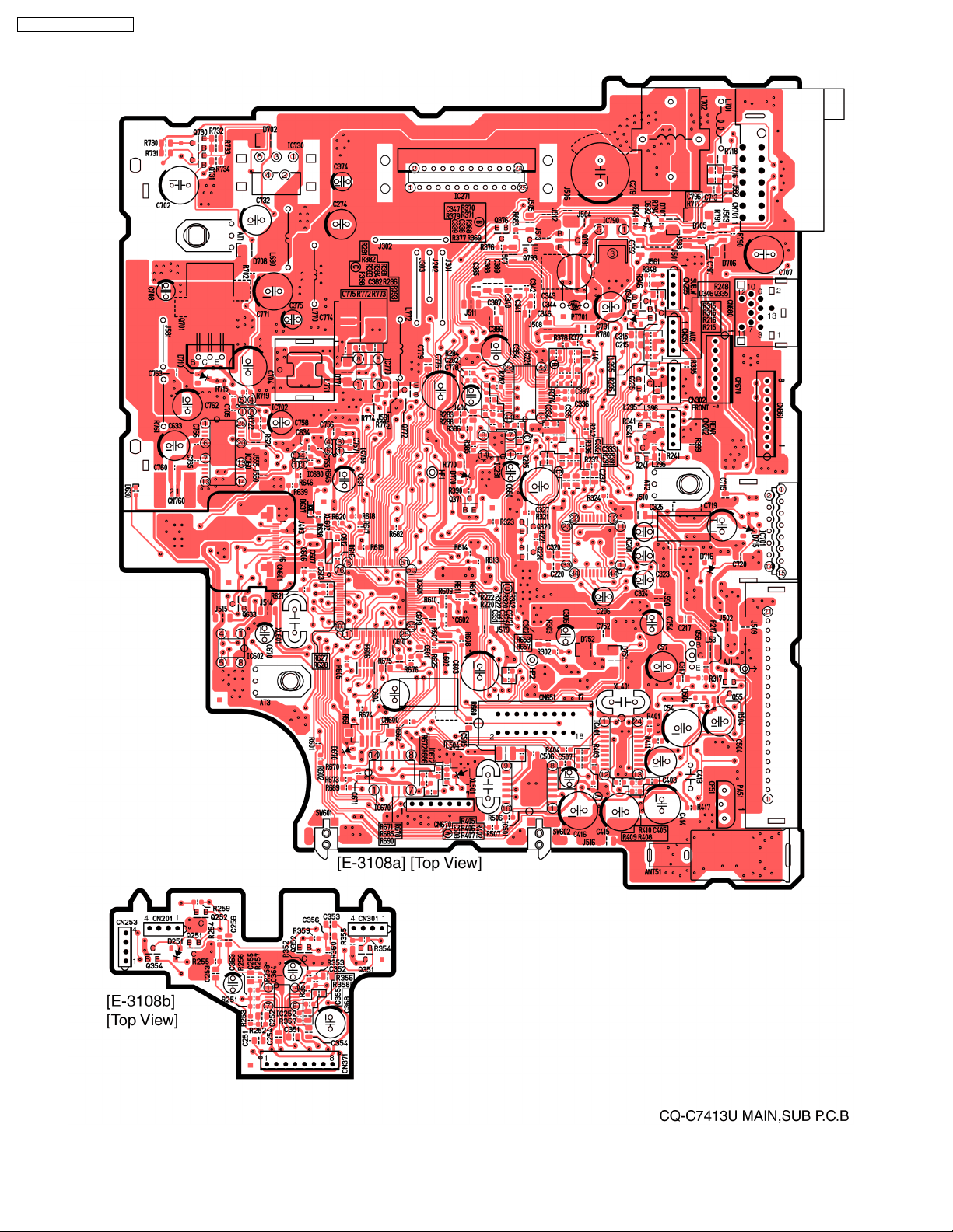
CQ-C7413U / CQ-C7113U
19.2. Main/Sub Block (Top View) [CQ-C7413U]
36

19.3. Main/Sub Block (Bottom View) [CQ-C7413U]
CQ-C7413U / CQ-C7113U
37
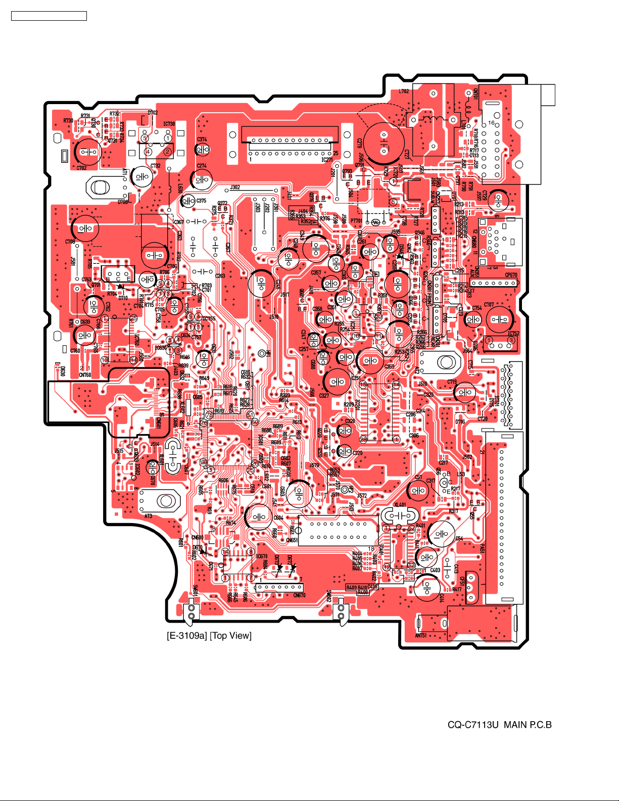
CQ-C7413U / CQ-C7113U
19.4. Main Block (Top View) [CQ-C7113U]
38

19.5. Main Block (Bottom View) [CQ-C7113U]
CQ-C7413U / CQ-C7113U
39

CQ-C7413U / CQ-C7113U
19.6. CD Servo Block (Top View)
40

19.7. CD Servo Block (Bottom View)
CQ-C7413U / CQ-C7113U
41

CQ-C7413U / CQ-C7113U
20 SCHEMATIC DIAGRAM-1
20.1. Sub Block [CQ-C7413U]
42

21 SCHEMATIC DIAGRAM-2
21.1. Main-1 Block [CQ-C7413U]
CQ-C7413U / CQ-C7113U
43

CQ-C7413U / CQ-C7113U
21.2. Main-2 Block [CQ-C7413U]
44

21.3. Main Block [CQ-C7113U]
CQ-C7413U / CQ-C7113U
45

CQ-C7413U / CQ-C7113U
21.4. Display Block [CQ-C7413U]
46

21.5. Display Block [CQ-C7113U]
CQ-C7413U / CQ-C7113U
47

CQ-C7413U / CQ-C7113U
21.6. CD Servo Block
3.1
2.5
YESAN086
1.8
3032-14-35
1.5
0
1.6
1.6
1.6
1.6
1.8
1.5
1.6
1.5
1.6
1.3
1.3
3.3
3.3
2.5
0.2
1.6
1.8
1.6
1.8
0.6
1.8
0
0
2.0
2.0
1.602.2
1.6
1.6
3.3
1.6
1.4
1.6
YESAM343
3.3
1.6
0
2.3
1.6
1.6
1.6
1.6
1.6
1.5
1.7
0
000
1.5
001.6
00000
0.7
0
0
3.3
0
0
3.3
0
3.2
2.6
2.8
2.8
2.9
2.8
2.9
0
1.5
3.3
0
0
1.6
1.6
3.3
1.6
0
0
0
0
1.5
0
1.5
1.6
L
R
2.8
2.8
2.8
2.8
2.9
3.2
0
0
3.2
3.2
0
0
3.2
2.6
3.2
0
3.2
2V/DIV,5ms/DIV
YESAM337
3.2
3.0
1.3
2V/DIV,1ms/DIV
2.3
0.5V/DIV,0.1µs/DIV
1.3
0
0
2.1
0.3
3.3V3.3V
3.2
3.2
0
0
3.2
2.9
0
0.5
0
2V/DIV,5ms/DIV
0
0
3.2
3.2
0
0
3.2
3.3V
To Optical Pic Up A'ssy
The following symbols are
shown on the schematic diagram.
3.3V
8V
8V
3.3V
CD(L,R)
YESAM339
3.3
B1GDCFJJ008
YESAN116
YESAN116
L
0
R
3.3V
L
YESAM342
3.2
8.0
3.3V
8V
3.3V 3.3V
R
8V
1.6
1.6
1.6
0
0
3.204.4
4.3
4.5
4.2
7.9
0
4.1
4.0
3.4
3.5
0
7.9
1.7
1.1
1.4
3.2
8.0
1.6
8V
3.2
3.2
3.3V
8V
3.2
0
3.2
1.5
YESAM341
3.3V
3.3V
8V8V
L
R
3.2
0
3.2
1.5
YESAM341
To
MAIN
CN651
48
CQ-C7413U/C7113U CD DECK

22 BLOCK DIAGRAM
22.1. Main-1/Sub Block [CQ-C7413U]
CQ-C7413U / CQ-C7113U
49

CQ-C7413U / CQ-C7113U
22.2. Main-2/ Display Block [CQ-C7413U]
50

22.3. Main-1 Block [CQ-C7113U]
CQ-C7413U / CQ-C7113U
51

CQ-C7413U / CQ-C7113U
22.4. Main-2/ Display Block [CQ-C7113U]
52

22.5. CD Servo Block
CQ-C7413U / CQ-C7113U
53

21 SCHEMATIC DIAGRAM-2
21.1. Main-1 Block [CQ-C7413U]
43

CQ-C7413U / CQ-C7113U
43

CQ-C7413U / CQ-C7113 U
21.2. Main-2 Block [CQ-C7413U]
44

44

21.3. Main Block [CQ-C7113U]
45

CQ-C7413U / CQ-C7113U
45

CQ-C7413U / CQ-C7113 U
21.4. Display Block [CQ-C7413U]
46

46

21.5. Display Block [CQ-C7113U]
47

CQ-C7413U / CQ-C7113U
47

CQ-C7413U / CQ-C7113 U
21.6. CD Servo Block
3.1
2.5
YESAN086
1.8
3032-14-35
1.5
0
1.6
1.6
1.6
1.6
1.8
1.5
1.6
1.5
1.6
1.3
1.3
3.3
3.3
2.5
0.2
1.6
1.8
1.6
1.8
0.6
1.8
0
0
2.0
2.0
1.602.2
1.6
1.6
3.3
1.4
1.6
1.6
YESAM343
3.3
1.6
0
2.3
1.6
1.6
1.6
1.6
1.6
1.5
1.7
0
000
1.5
001.6
00000
0.7
0
0
3.3
0
0
3.3
0
3.2
2.6
2.8
2.8
2.9
2.8
2.9
0
1.5
3.3
0
0
1.6
1.6
3.3
1.6
0
0
0
0
1.5
0
1.5
1.6
L
R
To Optical Pic Up A'ssy
The following symbols are
shown on the schematic diagram.
3.3V
8V
8V
3.3V
CD(L,R)
YESAM339
B1GDCFJJ008
YESAN116
8V
1.6
1.6
1.6
0
0
3.204.4
4.3
4.5
4.2
7.9
0
4.1
4.0
3.4
3.5
0
7.9
1.7
1.1
1.4
3.2
8.0
1.6
8V
3.2
3.2
3.3V
YESAN1
8V
48

2-14-35
0.5V/DIV,0.1µs/DIV
3.3V3.3V
2.8
0
2.8
2.8
2.8
2.9
3.2
0
0
3.2
3.2
0
0
3.2
2V/DIV,5ms/DIV
YESAM337
3.0
1.3
2V/DIV,1ms/DIV
2.3
1.3
0
0
0
3.2
2.9
0
0.5
0
2V/DIV,5ms/DIV
0
0
3.2
3.2
0
0
0
3.2
2.1
0.3
3.2
3.2
3.2
3.2
3.2
2.6
3.3V
B1GDCFJJ008
YESAN116
3.3
YESAN116
L
0
R
3.3V
L
YESAM342
3.2
8.0
3.3V
8V
3.3V 3.3V
R
8V
3.2
0
3.2
1.5
YESAM341
3.3V
3.3V
8V8V
L
To
MAIN
CN651
R
3.2
0
3.2
1.5
YESAM341
48
CQ-C7413U/C7113U CD DECK
 Loading...