

Panasonic CNZ1413 Datasheet
Integrated Photosensors
CNZ1413
Integrated Photosensors
Overview
CNZ1413 are ultraminiature, highly reliable transmissive
photosensors consisting of a high-efficiency GaAs infrared light
emitting diode chip that is integrated with a high-sensitivity Siintegrated-photodetector chip in a double molded resin package.
Features
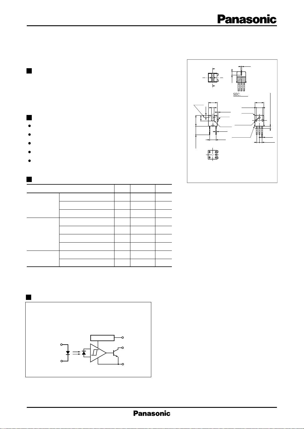
Ultraminiature : 4.2 × 4.2 mm (height : 5.2 mm)
Fast response : t
Highly precise position detection (slit width : 0.3 mm)
Gap width : 1.2 mm
With attachment positioning pin
Absolute Maximum Ratings (Ta = 25˚C)
Parameter
Input (Light
emitting diode)
Output
(Photo IC)
Temperature
*1
Input power derating ratio is 1.0 mW/˚C at Ta ≥ 25˚C.
*2
Output power derating ratio is 2.67 mW/˚C at Ta ≥ 25˚C.
PHL
= 2.5µs, t
= 6 µs (typ.) (ON1413A)
PLH
Symbol
Reverse voltage (DC) V
Forward current (DC) I
Power dissipation P
Output current I
Output voltage V
Supply voltage V
Power dissipation P
Operating ambient temperature
Storage temperature
R
F
*1
D
O
O
CC
*2
C
T
opr
T
stg
Ratings Unit
6V
50 mA
75 mW
20 mA
30 V
17 V
200 mW
–25 to +85 ˚C
– 40 to +100
˚C
A
A'
Device
4.2±0.1
center
1.2
+0.15
0.5
(R0.1)
(2-C0.3)
2-0.25
*3.2
3
4
5
–0
(1.0)
3.0
5.2
4.0 min.
1
2
(Note)
1. Tolerance unless otherwise specified is ±0.2
2. ( ) Dimension is reference
3. * is dimension at the root of leads
4. Burrs should be less than 0.15mm
(0.3)
(1.5)
SEC. A-A'
3.0±0.05
(2-C0.3)
2-ø0.8±0.05
Gate the rest
0.3 max.
1: Anode 4: V
2: Cathode 5: GND
3: V
CC
Unit : mm
4.2
Not soldered 1.0 max.
3-0.5
*2-1.27
O
Pin Connection
CNZ1413
(Normally ON type)
Anode 1
Cathode 2
Const. Voltage Cir.
3 V
CC
4 V
O
5 GND
1
CNZ1413 Integrated Photosensors
Electrical Characteristics (Ta = 25˚C)
Parameter Symbol Conditions min typ max Unit
Input
characteristics
Forward voltage (DC)
Reverse current (DC)
“H” Output current
Output
characteristics
“L” Output voltage V
Operating power voltage V
Low-level supply current
High-level supply current
Threshold input current I
Transfer
characteristics
Note) Normally ON type characteristics is shown, ( ) shows Normally OFF type.
*
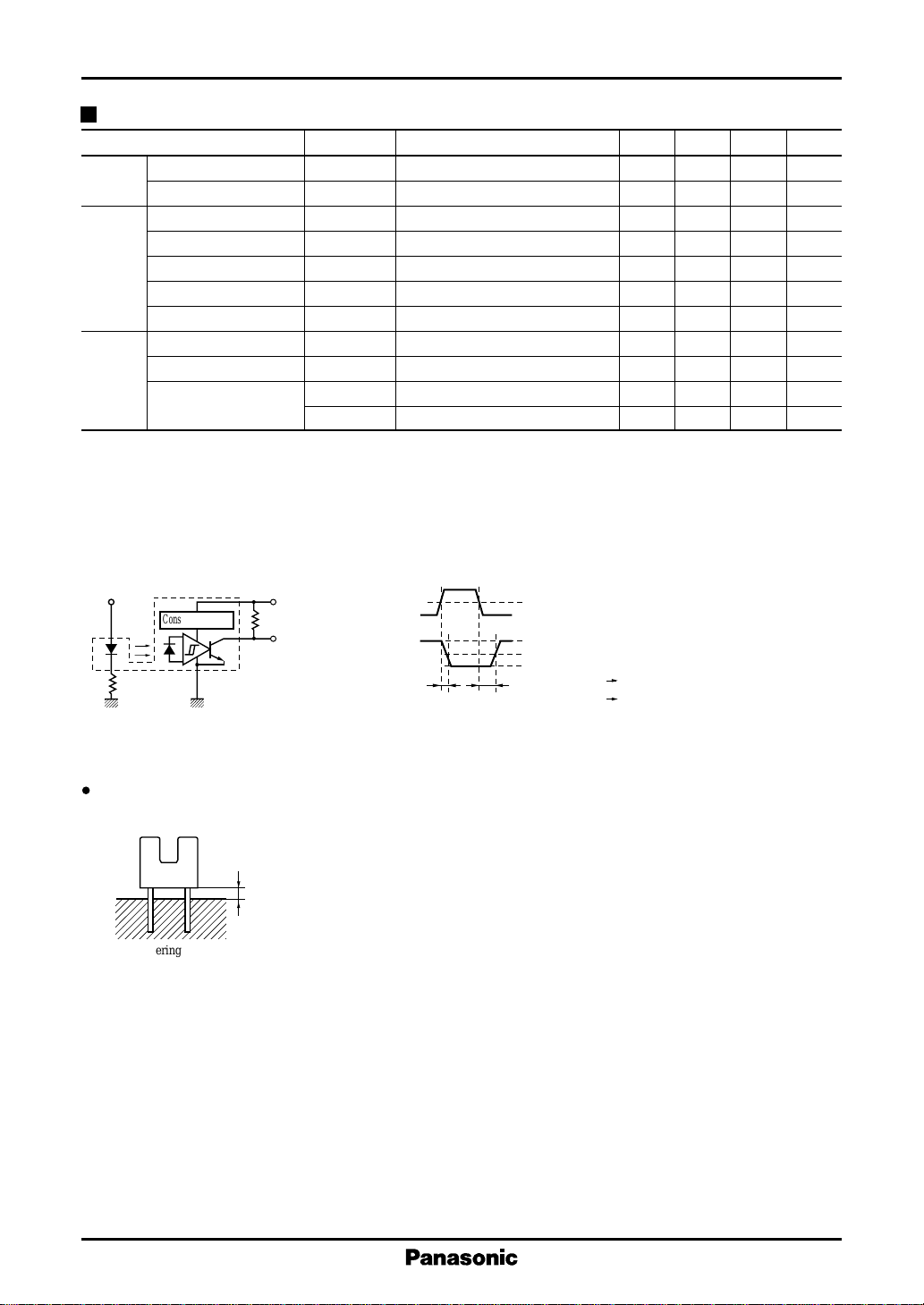
Switching time measurement circuit
Hysteresis
Response time
V
F
I
R
I
OH
OL
CC
I
CCL
I
CCH
FH→L(IFL→H
I
FLH/IFHL(IFHL/IFLH
t
)*V
PHL(tPLH
t
)*V
PLH(tPHL
IF = 20mA 1.2 1.4 V
VR = 3V 10 µA
V
V
= 5V, V
CC
= 5V, I
CC
= 30V, IF = 0mA
OH
= 20mA, IF = 5mA
OL
100 µA
0.15 0.4 V
4.5 17 V
V
= 5V, IF = 5mA 2.4 5 mA
CC
V
= 5V, IF = 0mA 0.8 3 mA
CC
)
V
= 5V 5 mA
CC
)
V
CC
CC
CC
= 5V
= 5V, I
= 5mA, RL = 1kΩ 2.5(3.5)
F
= 5V, I
= 5mA, RL = 1kΩ 6(5)
FP
0.7
µs
µs
Sig.IN
Const. Voltage Cir.
50Ω
V
CC
RL = 1kΩ
Sig.OUT
(Input pulse)
(Output pulse)
t
PHLtPLH
50%
V
OH
1.5V
V
OL
t
: H L Propagation time
PHL
: L H Propagation time
t
PLH
Important Information for Soldering
1. Soldering Position
A : Make sure the distance is 0.1 mm or more.
A
Soldering bath
2. Solder Temperature and Soldering Time
Temperature : 260˚C or less
Time : within 3 seconds
Note) Avoid using reflow soldering methods.
3. Other Issues
1) Soldering should not create excessive thermal or mechanical stress on the case package or leads.
Excessive stress may cause changes in the shape or characteristics of the package or leads.
2) Be careful not to allow solder, flux, solvents, etc. to remain on the case package.
Doing so may cause problems related to transmission characteristics, etc.
2
 Loading...