Panasonic CNC1S171 Datasheet

Optoisolators (Photocouplers)
CNC1S171
Optoisolator
For isolated signal transmission
Features
High current transfer ratio : CTR >50%
High I/O isolation voltage :
V
= 5000 V
ISO
Fast response :
t
= 2 µs, tf = 3 µs(typ.)
r
Low dark current : I
VDE approved (VDE0884)
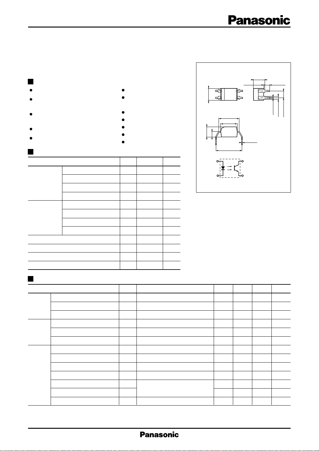
Absolute Maximum Ratings (Ta = 25˚C)
Input (Light
emitting diode)
Output (Photo
transistor)
Isolation voltage, input to output
Total power dissipation
Operating ambient temperature
Storage temperature
(min.)
rms
< 100nA
CEO
Parameter
Reverse voltage (DC)
Forward current (DC)
Pulse forward current
Power dissipation
Collector current
Collector to emitter voltage
Emitter to collector voltage
Collector power dissipation
Symbol
V
I
FP
P
V
V
P
V
T
T
UL listed (No. E79920)
BSI certified
(BS415 No. 7889, BS7002 No. 7890)
SEMKO certified (No. 9625004)
DEMKO certified (No. 305848)
NEMKO
certified
(No. 199633176)
FIMKO certified (No. 191784)
CSA approved (No. CA109151)
3.85±0.3
Ratings Unit
6V
50 mA
1A
75 mW
50 mA
80 V
7V
150 mW
5000 V
200 mW
–30 to +100
–55 to +125
˚C
˚C
rms
*1
Pulse width ≤ 100 µs, repeat 100 pps
*2
Input power derating ratio is
0.75 mW/˚C at Ta ≥ 25˚C.
*3
Output power derating ratio is
1.5 mW/˚C at Ta ≥ 25˚C.
I
F
D
I
C
CEO
ECO
C
ISO
P
opr
stg
R
*1
*2
*3
T
5.0 max.
1
2
4.58±0.3
7.62±0.3
6.2±0.5
2.0
10~12
14
23
Pin connection
4
3
0.25
+0.15
–0
Unit : mm
2.54 min.0.3 min.
4-0.5±0.1
4-1.2±0.15
2.54±0.25
1: Anode
2: Cathode
3: Emitter
4: Collector
Electrical Characteristics (Ta = 25˚C)
Parameter
Input
characteristics
Reverse current (DC)
Forward voltage (DC)
Capacitance between pins
Output
characteristics
Collector cutoff current
Collector to emitter voltage
Collector to emitter capacitance
DC current transfer ratio
Isolation voltage, input to output
Transfer
characteristics
Isolation capacitance, input to output
Isolation resistance, input to output
Rise time
Fall time
Collector to emitter saturation voltage
*1
DC current transfer ratio (CTR) is a ratio of output current against DC input current.
*2
tr : Time required for the collector current to increase from 10% to 90% of its final value
*3
tf : Time required for the collector current to decrease from 90% to 10% of its initial value
Symbol
Conditions min typ max Unit
IRVR = 3V 10 µA
VFIF = 50mA 1.35 1.5 V
CtVR = 0V, f = 1MHz 15 pF
I
CEOVCE
V
CEOIC
CCV
CTR
V
ISOt
C
ISOf
R
ISOVISO
*2
t
r
*3
t
f
V
CE(sat)IF
= 20V 5 100 nA
= 100µA80V
= 10V, f = 1MHz 10 pF
CE
*1*4
V
= 10V, IF = 5mA 50 600 %
CE
= 1 min., RH < 60% 5000 V
= 1MHz 0.7 pF
= 500V 10
V
= 10V, IC = 5mA, 2 µs
CC
RL = 100Ω 3 µs
= 20mA, IC = 1mA 0.1 0.2 V
rms
11
Ω
1

CNC1S171 Optoisolators (Photocouplers)
*4
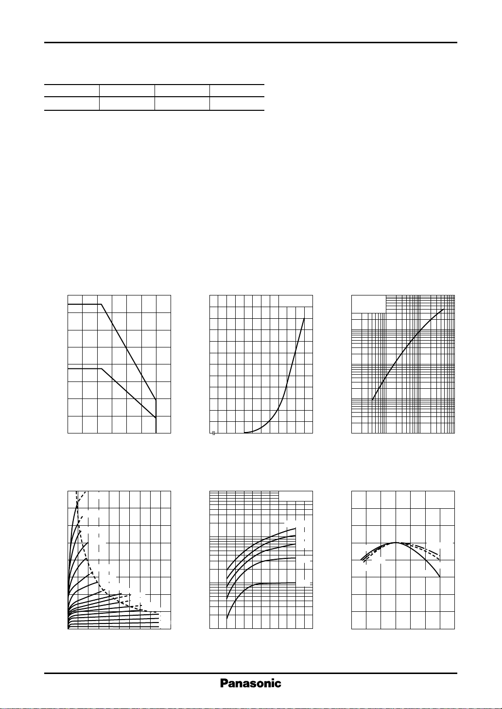
CTR classifications
Class Q R S
CTR (%) 50 to 120 100 to 250 200 to 600
PC , P
160
(mW)
D
, P
C
120
Collector power dissipation , power dissipation P
P
C
80
P
D
40
0
0 20406080 120
– 20 100
— Ta
D
Ambient temperature Ta (˚C )
I
— V
C
10mA
9mA
CE
8mA
7mA
6mA
5mA
4mA
3mA
2mA
1mA
40
30
(mA)
C
20
10
Collector current I
50mA
40mA
30mA
25mA
20mA
0
81624 4032
0
15mA
12mA
Collector to emitter voltage VCE (V)
I
— V
F
60
50
40
(mA)
F
30
20
F
Ta = 25˚C
Forward current I
10
0
0.9 1.0 1.1 1.2 1.41.3
0
Forward voltage VF (V)
I
— V
C
10
10
(mA)
C
2
1
CE(sat)
Ta = 25˚C
IF = 50mA
Collector current I
–1
10
0 0.2 0.4 0.60.1 0.3 0.5
Collector to emitter saturation voltage V
20mA
10mA
5mA
2mA
CE(sat)
2
10
10
(mA)
C
1
–1
10
Collector current I
–2
10
10
160
120
(%)
C
80
40
Relative output current I
0
– 50
(V)
I
— I
C
F
VCC = 10V
Ta = 25˚C
–1
11010
Forward current IF (mA)
I
— Ta
C
1mA
5mA
10mA
0 10050
1mA
Ambient temperature Ta (˚C )
= 5V
V
CC
IF = 10mA
5mA
2
2
 Loading...