

Panasonic CNA1311K Datasheet
Transmissive Photosensors (Photo Interrupters)
more than 1mm
Soldering bath
CNA131 1K
Photo Interrupter
For contactless SW, object detection
Overview
CNA1311K is an ultraminiature, highly reliable transmissive
photosensor in which a high efficiency GaAs infrared light emitting diode
chip and a high sensitivity Si phototransistor chip are integrated in a
double molded resin package.
Features
Ultraminiature : 2.6 × 4.0 mm (height : 3.3 mm)
Highly precise position detection : 0.05 mm
Gap width : 1.0 mm
Absolute Maximum Ratings (Ta = 25˚C)
Parameter
Input (Light
emitting diode)
Reverse voltage (DC) V
Forward current (DC) I
Power dissipation P
Collector current I
Output (Photo
transistor)
Collector to emitter voltage
Emitter to collector voltage
Collector power dissipation
Operating ambient temperature
Temperature Storage temperature T
Soldering temperature T
Symbol
R
F
*1
D
C
V
CEO
V
ECO
*2
P
C
T
opr
stg
*3
sol
Ratings Unit
6V
50 mA
75 mW
20 mA
35 V
6V
75 mW
–25 to +85 ˚C
–40 to +100
˚C
260 ˚C
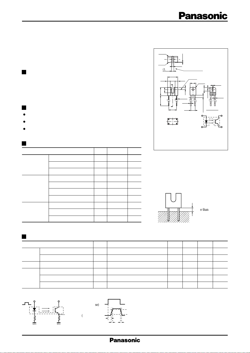
B side
A side
(1.8)
1.5 1.0 1.5
2.3
3.3
5.0 min.
(Note)
1. Tolerance unless otherwise specified is ±0.2
2. ( ) Dimension is reference
3. * is dimension at the root of leads
*1
Input power derating ratio is
(1.5)
4.0
A
A'
*3.0
13
24
(0.15)
With gate
A Side or B Side
(0.9)
+0.2
2-0.2
–0.1
2-0.4
*2.0
Optical
center
2.6
(C0.5)
1.5
1.0 max.
Not soldered
13
24
1: Anode
2: Cathode
1.0mW/˚C at Ta ≥ 25˚C.
*2
Output power derating ratio is
1.0mW/˚C at Ta ≥ 25˚C.
*3
Soldering time is within 5 seconds.
Unit : mm
Slit width
(0.15)
(0.45)
SEC. A-A'
Pin connection
3: Collecter
4: Emitter
2-0.5
Electrical Characteristics (Ta = 25˚C)
Parameter
Input
characteristics
Output characteristics
Transfer
characteristics
*
Switching time measurement circuit
50Ω R
Forward voltage (DC) VFIF = 20mA 1.2 1.4 V
Reverse current (DC) IRVR = 3V 10 µA
Collector cutoff current I
Collector current ICV
Collector to emitter saturation voltage
Response time tr , t
Sig.IN
V
CC
Sig.OUT 10%
L
(Input pulse)
(Output pulse)
Symbol
CEOVCE
V
CE(sat)IF
*
f
t
d
Conditions min typ max Unit
= 20V 100 nA
= 5V, IF = 5mA 50 600 µA
CE
= 10mA, IC = 40µA 0.4 V
V
= 5V, IC = 0.1mA, RL = 1000Ω
CC
td : Delay time
: Rise time (Time required for the collector current to increase
t
90%
r
from 10% to 90% of its final value)
: Fall time (Time required for the collector current to decrease
t
t
r
t
f
f
from 90% to 10% of its initial value)
50 µs
1

CNA1311K Transmissive Photosensors (Photo Interrupters)
IF , I
— Ta
60
(mA)
C
50
, I
F
40
30
20
10
Forward current, collector current I
0
0 20406080100
– 25
C
I
F
I
C
Ambient temperature Ta (˚C )
V
— Ta
F
IF = 50mA
(V)
F
1.6
1.2
0.8
10mA
1mA
60
50
40
(mA)
F
30
20
Forward current I
10
0
0.4 0.8 1.2 1.6 2.42.0
0
Forward voltage VF (V)
3
2
(mA)
C
I
I
F
C
— V
— V
F
CE
Ta = 25˚C
Ta = 25˚C
IF = 20mA
5
4
(mA)
C
3
2
Collector current I
1
0
5 10152025
0
Forward current IF (mA)
120
100
(%)
C
80
60
I
I
C
— I
C
— Ta
F
= 5V
V
CE
Ta = 25˚C
V
= 5V
CE
= 5mA
I
F
Forward voltage V
0.4
0
– 40 – 20
0 20406080100
Ambient temperature Ta (˚C )
I
1
VCE = 20V
–1
10
(µA)
–2
10
CEO
–3
10
Dark current I
–4
10
–5
10
CEO
0 20406080100– 40 – 20
Ambient temperature Ta (˚C )
— Ta
1
Collector current I
0
1234 65
0
Collector to emitter voltage VCE (V)
t
— I
r
3
10
2
10
(µs)
r
10
C
Rise time t
V
Sig.IN
Sig.
50Ω
CC
Sig.
OUT
R
L
–1
1
OUT
–1
10
–2
10
Collector current IC (mA)
VCC = 5V
RL = 2kΩ
1kΩ
100Ω
t
d
trt
11010
15mA
10mA
5mA
2mA
90%
10%
f
40
Relative output current I
20
0
0 20406080100– 40 – 20
Ambient temperature Ta (˚C )
t
— I
3
10
2
10
(µs)
f
10
f
Fall time t
V
Sig.IN
1
Sig.
OUT
–1
10
50Ω
–2
–1
10
Collector current IC (mA)
C
VCC = 5V
RL = 2kΩ
1kΩ
100Ω
CC
90%
10%
t
d
t
t
r
f
11010
R
Sig.
OUT
L
2
 Loading...