

Panasonic CNA1303K Datasheet
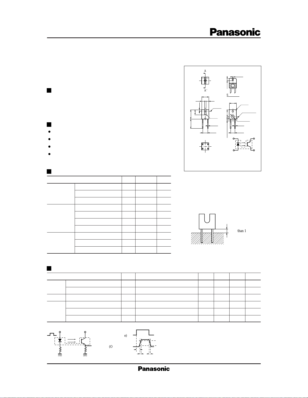
Transmissive Photosensors (Photo Interrupters)
more than 1mm
Soldering bath
ON1003
Photo Interrupter
For contactless SW, object detection
A
Slit width
(0.3)
Unit : mm
Outline
ON1003 is an ultraminiature, highly reliable transmittive
photosensor in which a high efficiency GaAs infrared light emitting
diode chip and a high sensitivity Si phototransistor chip are integrated
in a double molded resin package.
Features
Ultraminiature : 4.2 × 4.2 mm (height : 5.2 mm)
Fast response : tr, tf = 35 µs (typ.)
Highly precise position detection : 0.15 mm
Gap width : 1.2 mm
Absolute Maximum Ratings (Ta = 25˚C)
Parameter
Input (Light
emitting diode)
Reverse voltage (DC) V
Forward current (DC) I
Power dissipation P
Collector current I
Output (Photo
transistor)
Collector to emitter voltage
Emitter to collector voltage
Collector power dissipation
Operating ambient temperature
Temperature Storage temperature T
Soldering temperature T
Symbol
R
F
*1
D
C
V
CEO
V
ECO
*2
P
C
T
opr
stg
*3
sol
Ratings Unit
6V
50 mA
75 mW
20 mA
35 V
6V
75 mW
–25 to +85 ˚C
– 40 to +100
˚C
260 ˚C
Device
center
(1.5)
SEC. A-A'
4.2
3.9
1.0 max.
Not soldered
24
13
Pin connection
A'
4.2
1.5 1.5
1.2
(1.0)
2.8
5.2
4.0 min.
(Note)
1. Tolerance unless otherwise specified is ±0.2
2. ( ) Dimension is reference
3. * is dimension at the root of leads
4. Burrs should be less than 0.15mm
*1
Input power derating ratio is
(C0.3)
2-0.25
*3.2
13
24
1.0mW/˚C at Ta ≥ 25˚C.
*2
Output power derating ratio is
1.0mW/˚C at Ta ≥ 25˚C.
*3
Soldering time is within 5 seconds.
(C0.5)
Gate the rest
ø1.5
2-0.5
*2.54
0.3 max.
+0.1
–0
Electrical Characteristics (Ta = 25˚C)
Parameter
Input
characteristics
Output characteristics
Transfer
characteristics
*
Switching time measurement circuit
50Ω R
Forward voltage (DC) VFIF = 20mA 1.2 1.4 V
Reverse current (DC) IRVR = 3V 10 µA
Collector cutoff current I
Collector current ICV
Collector to emitter saturation voltage
Response time tr , t
Sig.IN
V
CC
Sig.OUT 10%
L
Symbol
V
CE(sat)IF
(Input pulse)
(Output pulse)
CEOVCE
CE
= 10mA, IC = 50µA 0.4 V
*
V
f
CC
t
d
t
r
Conditions min typ max Unit
= 20V 100 nA
= 5V, IF = 5mA 100 1300 µA
= 5V, IC = 0.1mA, RL = 1000Ω
td : Delay time
: Rise time (Time required for the collector current to increase
t
90%
r
from 10% to 90% of its final value)
: Fall time (Time required for the collector current to decrease
t
t
f
f
from 90% to 10% of its initial value)
35 µs
1
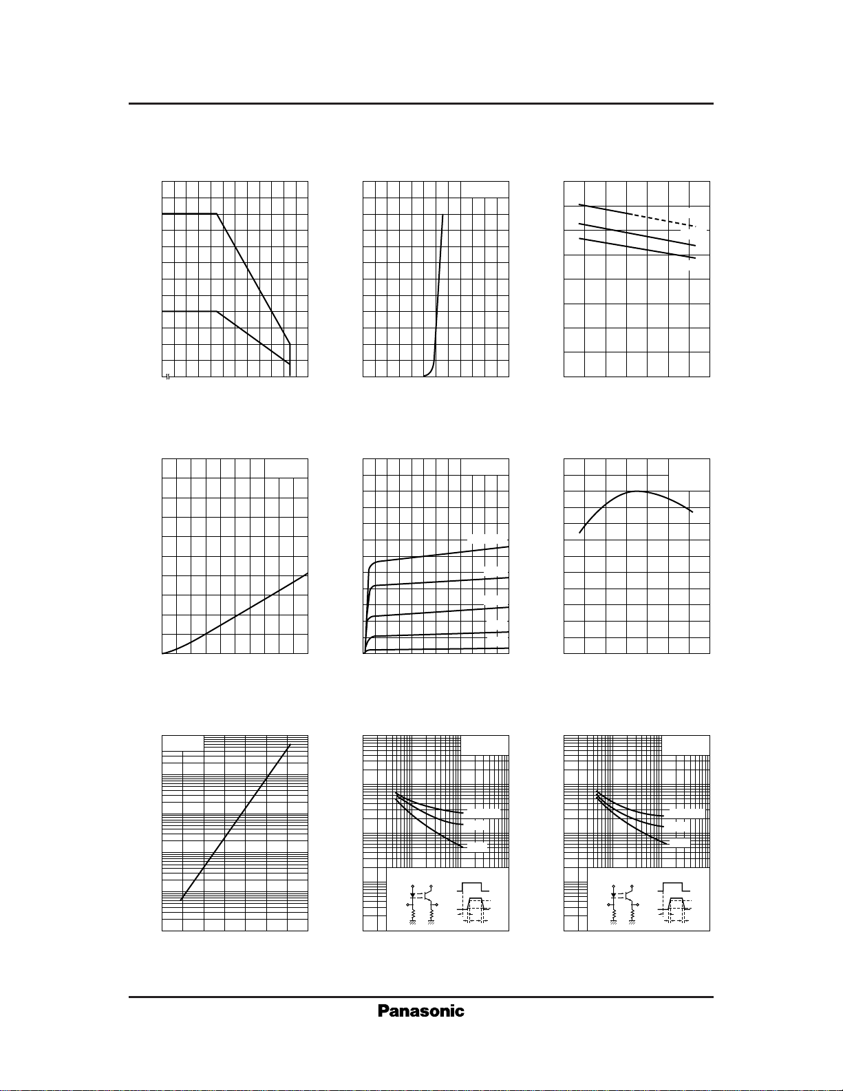
Transmissive Photosensors (Photo Interrupters) ON1003
— Ta
IF , I
60
(mA)
C
50
, I
F
40
30
20
10
Forward current, collector current I
0
0 20406080100
– 25
C
I
F
I
C
Ambient temperature Ta (˚C )
— I
I
C
5
4
(mA)
C
3
2
Collector current I
1
0
5 10152025
0
F
V
Ta = 25˚C
Forward current IF (mA)
CE
= 5V
— V
I
F
60
50
40
(mA)
F
30
20
F
Forward current I
10
0
0.4 0.8 1.2 1.6 2.42.0
0
Forward voltage VF (V)
— V
I
C
CE
(mA)
C
3
2
1
Collector current I
0
1234 65
0
Collector to emitter voltage VCE (V)
Ta = 25˚C
Ta = 25˚C
IF = 20mA
15mA
10mA
5mA
2mA
— Ta
V
1.6
1.2
(V)
F
0.8
Forward voltage V
0.4
0
– 40 – 20
F
0 20406080100
Ambient temperature Ta (˚C )
— Ta
I
120
100
(%)
C
80
60
40
Relative output current I
20
0
C
0 20406080100– 40 – 20
Ambient temperature Ta (˚C )
IF = 50mA
10mA
1mA
V
= 5V
CE
= 5mA
I
F
1
VCE = 20V
–1
10
(µA)
–2
10
CEO
–3
10
Dark current I
–4
10
–5
10
2
— Ta
I
CEO
0 20406080100– 40 – 20
Ambient temperature Ta (˚C )
3
10
2
10
(µs)
r
10
Rise time t
1
–1
10
–2
10
— I
t
r
C
VCC = 5V
Ta = 25˚C
RL = 2kΩ
1kΩ
100Ω
V
Sig.IN
CC
Sig.
OUT
50Ω
Sig.
OUT
t
d
R
L
t
–1
10
r
110
Collector current IC (mA)
t
90%
10%
f
3
10
2
10
(µs)
f
10
Fall time t
1
–1
10
–2
— I
t
f
C
VCC = 5V
Ta = 25˚C
RL = 2kΩ
1kΩ
100Ω
V
Sig.IN
CC
Sig.
OUT
50Ω
Sig.
OUT
t
R
–1
10
d
L
t
r
11010
Collector current IC (mA)
t
90%
10%
f
 Loading...