

查询CNA1009H供应商查询CNA1009H供应商
Transmissive Photosensors (Photo lnterrupters)
CNZ1021 (ON1021), CNZ1023 (ON1023),
CNA1009H (ON1024)
Photo lnterrupter
For contactless SW, object detection
■ Overview
CNZ1021, CNZ1023 and CNA1009H are a transmissive photosensor in which a high efficiency GaAs infrared light emitting diode is used as the light emitting element, and a high sensitivity phototransistor is used as
the light detecting element. The two elements are arranged so as to face each other, and objects passing be-
tween them are detected.
■ Features
• Highly precise position detection: 0.25 mm
• Gap width: 3 mm (CNZ1021, CNZ1023)
5 mm (CNA1009H)
• The type directly attached to PCB ....... CNZ1021
Screw-fastened type (one side) ............ CNZ1023
The type directly attached to PCB ....... CNA1009H
(with a positioning pins)
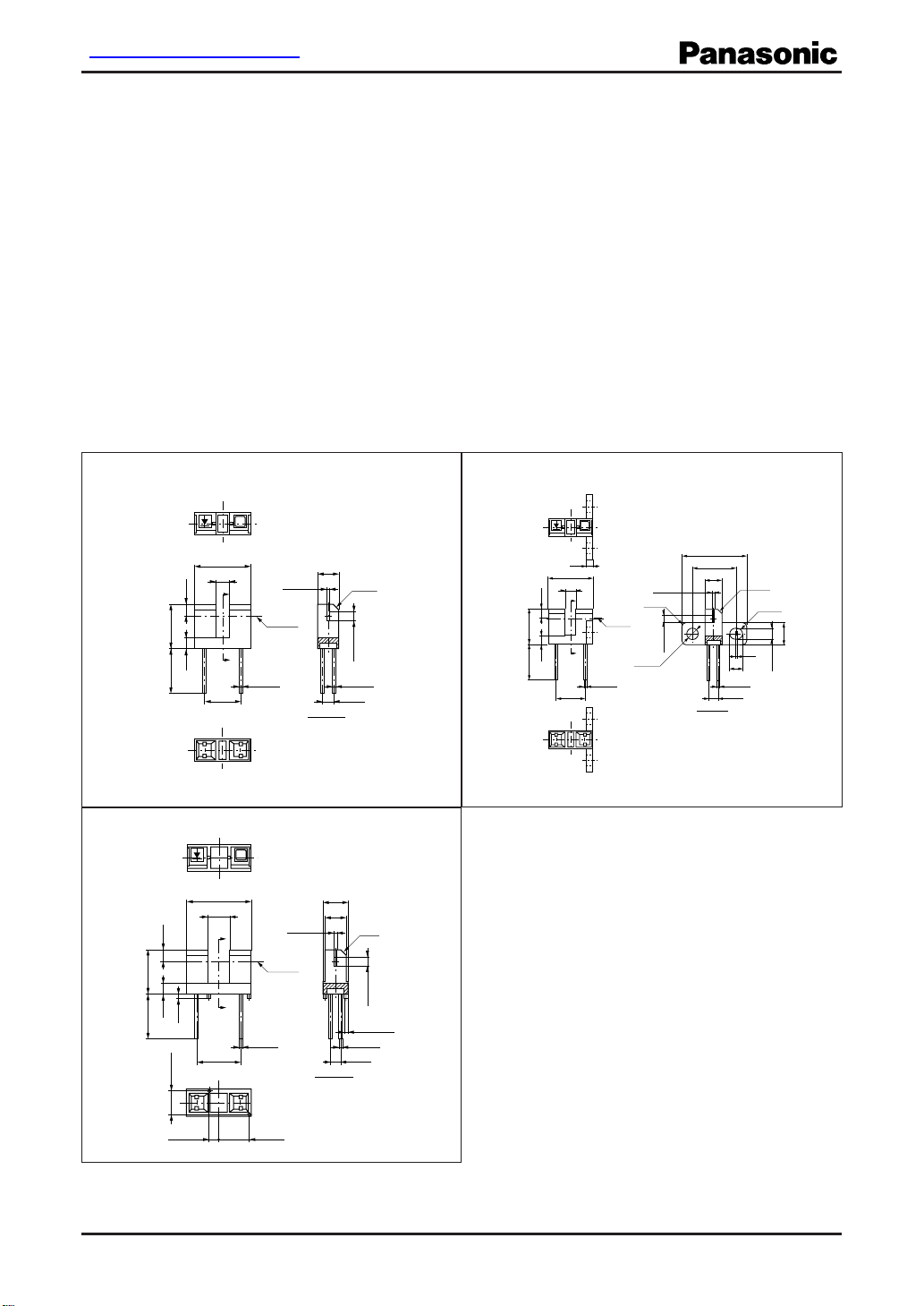
CNZ1023 Unit: mmCNZ1021 Unit: mm
Σ
12.0
3.0±0.15
A
(2.5)
10.0
A'
2.5
10.0 min.
(2-0.45) (2-0.45)
(7.6) (2.54)
23
0.4±0.1
Device
center
5.0
(C1.2)
2.1±0.15
SEC. A-A'
1: Anode
2: Cathode
14
3: Collector
4: Emitter
PISTR104-001 Package
CNA1009H Unit: mm
Σ
(2.5)2.5
10.0
10.0 min.
±0.1
5.2
14.0
5.0
±0.15
A
A'
2-0.7
(10.0)
23
(2-0.45)
Device
center
6.0
5.0
0.5
±0.1
SEC. A-A'
(C1)
2.2±0.15
2-φ0.7
(2-0.45)
(2.54)
±0.1
1: Anode
2: Cathode
14
2.35
±0.1
6.6
±0.1
3: Collector
4: Emitter
PISTR104-004 Package
(Note) 1. Tolerance unless otherwise specified is ±0.3
2. ( ) Dimension is reference
Note) The part numbers in the parenthesis show conventional part number.
Σ
2.0
12.0
3.0
±0.15
A
(2.5)
10.0
A'
2.5
10.0 min.
(2-0.45)
(7.6) (2.54)
23
14
Device
center
0.4
(4-R2)
+0.15
φ3.0
-
0
18.0
12.0±0.15
5.0
±0.1
2.1±0.15
SEC. A-A'
PISTR104-003 Package
3.5
(2-0.45)
(C1.2)
2-R1.5
0.5
6.0
0
+0.15
-
3.0
1: Anode
2: Cathode
3: Collector
4: Emitter
Publication date: April 2004 SHG00017BED
1

CNZ1021, CNZ1023, CNA1009H
■ Absolute Maximum Ratings Ta = 25°C
Parameter Symbol Rating Unit
Input (Light Reverse
emitting diode) voltage
CNZ1021 V
R
CNZ1023 3
CNA1009H 5
Forward current I
1
Power dissipation
*
Output (Photo Collector-emitter voltage V
P
CEO
F
D
transistor) (Base open)
Emitter-collector voltage V
ECO
(Base open)
Temperature
Collector current I
Collector power dissipation
Operating ambient temperature
Storage temperature T
C
2
*
P
C
T
opr
stg
Note)*1: Input power derating ratio is 1.0 mW/°C at Ta ≥ 25°C.
2: Output power derating ratio is 1.33 mW/°C at Ta ≥ 25°C.
*
■ Electrical-Optical Characteristics Ta = 25°C ± 3°C
Parameter Symbol Conditions Min Typ Max Unit
Input
characteristics
Output
characteristics
Transfer
characteristics
Note) 1. Input and output are practiced by electricity.
Forward voltage VFIF = 20 mA 1.25 1.40 V
Reverse current I
Collector-emitter cutoff current
R
I
CEO
(Base open)
Collector current I
Collector-emitter saturation voltage
Rise time
Fall time
*
*
C
V
CE(sat)IF
t
r
t
f
2. This device is designed be disregarded radiation.
3.*: Switching time measurement circuit
Sig. in
50 Ω R
V
CC
L
Sig. out
(Input pulse)
(Output pulse)
3V
50 mA
75 mW
30 V
5V
20 mA
100 mW
−25 to +85 °C
−40 to +100 °C
VR = 3 V 10 µA
VCE = 10 V 10 200 nA
VCC = 5 V, IF = 20 mA, RL = 100 Ω 0.5 15.0 mA
= 40 mA, IC = 1 mA 0.4 V
VCC = 5 V, IC = 1 mA 5 µs
RL = 100 Ω 5 µs
t
r
t
: Rise time
r
: Fall time
t
90%
f
10%
t
f
2
SHG00017BED
 Loading...