

Panasonic CF-29N3LGZBM Service Manual
ORDER NO. CPD0604069C1
Notebook Computer
CF-29
Model No. CF-29N3LGZBM
This is the Service Manual for
the following areas.
M …for U.S.A. and Canada
© 2006 Matsushita Electric Industrial Co., Ltd. All rights reserved.
Unauthorized copying and distribution is a violation of law.

WARNING
For U.K.
This apparatus must be earthed for your safety.
To ensure safe operation the three-pin plug must be inserted only into a standard three-pin power point
which is effectively earthed through the normal household wiring.
Extension cords used with the equipment must be three-core and be correctly wired to provide connection to earth. Wrongly wired extension cords are a major cause of fatalities.
The fact that the equipment operates satisfactorily does not imply that the power point is earthed and
that the installation is completely safe.
For your safety, if you have any doubt about the effective earthing of the power point, consult a qualified electrician.
FOR YOUR SAFETY PLEASE READ THE FOLLOWING TEXT CAREFULLY
This appliance is supplied with a moulded three pin mains plug for your safety and convenience.
A 3 amp fuse is fitted in this plug.
Should the fuse need to be replaced please ensure that the replacement fuse has a rating of 3 amps and
that it is approved by ASTA or BSI to BS 1362.
Check for the ASTA mark or the BSI mark on the body of the fuse.
If the plug contains a removable fuse cover you must ensure that it is refitted when the fuse is replaced.
If you lose the fuse cover the plug must not be used until a replacement cover is obtained.
A replacement fuse cover can be purchased from your local Panasonic Dealer.
IF THE FITTED MOULDED PLUG IS UNSUITABLE FOR THE SOCKET OUTLET IN YOUR
HOME THEN THE FUSE SHOULD BE REMOVED AND THE PLUG CUT OFF AND DISPOSED
OF SAFELY.
THERE IS A DANGER OF SEVERE ELECTRICAL SHOCK IF THE CUT OFF PLUG IS INSERTED
INTO ANY 13 AMP SOCKET.
If a new plug is to be fitted please observe the wiring code as shown below.
If in any doubt please consult a qualified electrician.
Warning: THIS APPLIANCE MUST BE EARTHED.
Important
The wires in this mains lead are coloured in accordance with the following code:
Green-and-yellow: Earth
Blue: Neutral
Brown: Live
As the colours of the wires in the mains lead of this apparatus may not correspond with the coloured
markings identifying the terminals in your plug, proceed as follows:
The wire which is coloured GREEN-and-YELLOW must be connected to the terminal in the plug
which is marked by the letter E or by the safety earth symbol
YELLOW.
The wire which is coloured Blue must be connected to the terminal which is marked with the letter N or
coloured BLACK.
The wire which is coloured Brown must be connected to the terminal which is marked with the letter L
or coloured RED.
coloured GREEN or GREEN-and-
The mains plug on this equipment must be used to disconnect the mains power.
Please ensure that a socket outlet is available near the equipment and shall be easily accessible.
How to replace the fuse
Open the fuse compartment with a screwdriver and replace the fuse.
Warnings
This equipment is not designed for connection to an IT power system.
(An IT system is a system having no direct connections between live parts and Earth; the exposed-conduciveparts of the electrical installation are earthed.
An IT system is not permitted where the computer is directly connected to public supply systems in the U.K.)
Disconnect the mains plug from the supply socket when the computer is not in use.
This equipment is produced to BS800/1983.
1

LASER SAFETY INFORMATION
For U.S.A.
Class 1 LASER-Product
This product is certified to comply with DHHS Rules 21 CFR Subchapter J.
This product complies with European Standard EN60825 (or IEC Publication 825)
For all areas
This equipment is classified as a class 1 level LASER product and there is no hazardous LASER radiation.
Caution:
(1) Use of controls or adjustments or performance of procedures other than those specified herein may result in
hazardous radiation exposure.
(2) The drive is designed to be incorporated into a computer-based system or unit which has an enclosing cover.
It should never be used as a stand alone drive.
Danger:
The serviceman should not remove the cover of drive unit and should not service because the drive unit is a nonserviceable part.
Please check DANGER label on PD-drive unit.
• Unplug the AC power cord to the equipment before opening the top cover of the drive.
When the power switch it on, do not place your eyes close to the front panel door to look into the interior of the unit.
LASER Specification
Class 1 level LASER Product
Wave Length: DVD 658±8 nm
CD 775~815 nm
Laser safety information is appropriate only when drive with laser is installed.
2
3
4

CONTENTS
1 Diagnosis Procedure ······································································································1-1
2 Power-On Self Test (Boot Check) ··················································································2-1
3 List of Error Codes ··········································································································3-1
4 Diagnostic Test ···············································································································4-1
5 Self Diagnosis Test ·········································································································5-1
6 Wiring Connection Diagram ···························································································6-1
7 Disassembly/Reassembly ······························································································7-1
8 Exploded View ················································································································8-1
9 Replacement Parts List ··································································································9-1
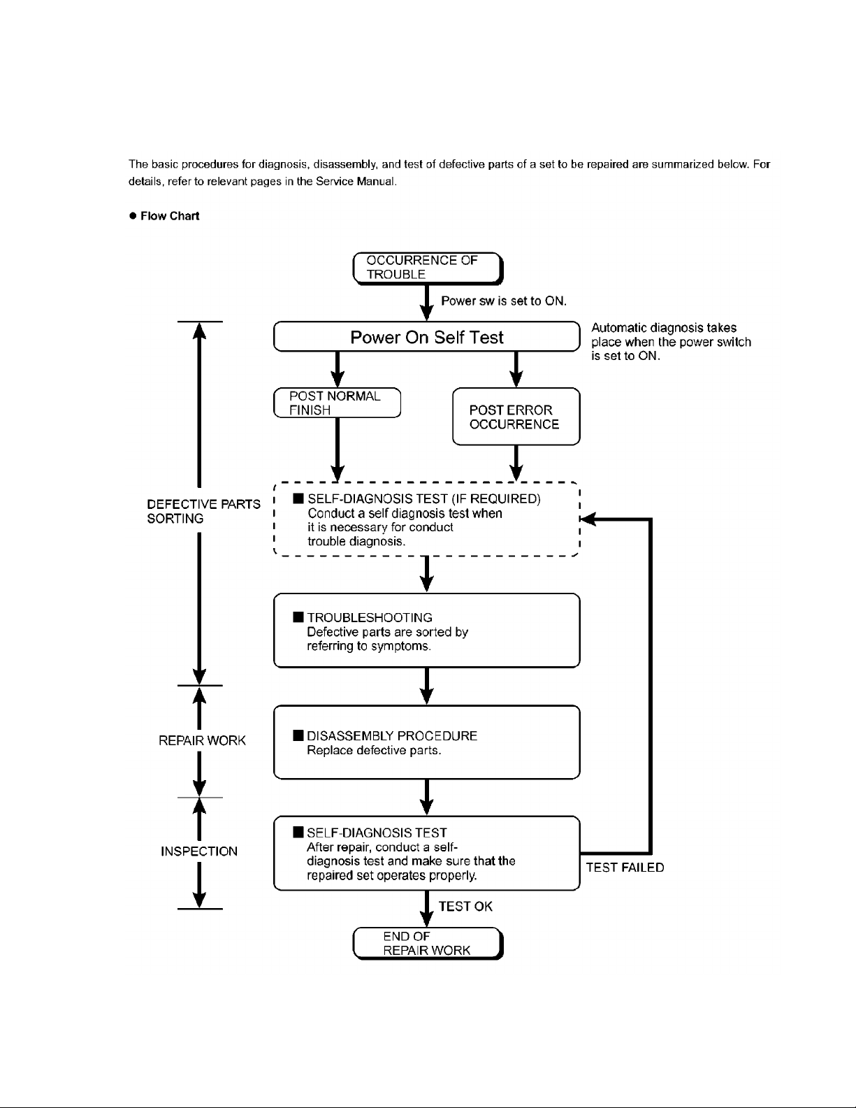
1 Diagnosis Procedure
1.1. Basic Procedure
1-1

f
k
c
1.2. Troubleshooting
Please take note of the following two points with regard to troubleshooting:
1. Know-how of diagnosis upon occurrence of heavy troubles, e.g. ‘Set cannot be turned ON’, ‘Set fails to start’, ‘No display on
screen’, etc.
2. Explanation of each trouble, mainly symptom of trouble in operation.
Flow Chart
START
START
Set cannot be supplied with current.
Power lamp fails to light up.
Dark display on screen.
Screen fails to display.
Failure in starting
Not displayed properly on screen.
Some or all keys cannot be input.
DVD/CD CALL not practicable.
*Clean DVD-ROM drive with an applicator.
Starts but operates unstably.
Pay attention to the following points when in pursuit of the cause of a troubleshooting.
1. Peripheral apparatus connected with the set should all be removed before operation check.
2. Make sure that cables, boards, etc. are not coming off, and recheck the contact condition.
AC
Adaptor/Battery
Output voltage
NG
Replace AC Adaptor/Battery
OK
Check contact condition of power input terminal. Replace i
YES
NO
defective.
Check Power SW. Replace if defective.
NG
Replace inverter board.
Check inverter cable continuity. Replace if defective
Power lamp
check
Inverter board
OK
YES
NO
Replace LCD back light.
NG
Replace LCD unit.
LCD back
light lighting
LCD unit
check
OK
BIOS operation
chec
NO
Replace main board (Check fuse at power source).
YES
Result of
POST
NG
Refer to POST
error code table.
Replace main board.
OK
Set-up utility
starting
NG
Replace main board.
OK
Return set-up utility setpoint to the state of ‘delivery from factory’.
Check HDD cable connection and continuity.
NO
HDD access
Main board
check
YES
NG
Replace if defective.
Replace HDD & Reinstall.
Replace main board.
Replace main board
OK
Make sure of contact of K/B connector in use.
Replace keyboard or main board.
Check if there are any flaws on DVD or CD
Trouble
symptoms on some
of DVD or CD
NO
media. Since flaws may appear on specifi
media, DVD or CD media can be defective.
YES
Replace DVD drive.
Replace main board.
Reinstall HDD.
Replace main board.
Heavy trouble e.g.,
‘Set cannot be turned
ON’, ‘Set fails to start’,
‘No display on
screen’, etc.
Each kind of
trouble in
operation.
START
END
1-2
2 Power-On Self Test (Boot Check)
Outline of POST
The set has a boot check function called POST (Power-On Self Test) in it. The condition of the main body is diagnosed by checking
beep sound or error code.
Start .............Test begins automatically when power switch is set to ON.
Normal finish .....After memory checking, a beep sound is issued once and the set is placed into automatic stop.
Note: If no error occurs, nothing is displayed. (No display of OK, etc.)
Error Diagnosis by Checking Beep Signal Sound
The beep sound is as follows:
(1 (long sound) -2-3-4)
(Length of bar shows length of sound.)
= long sound (about 0.4 sec.),
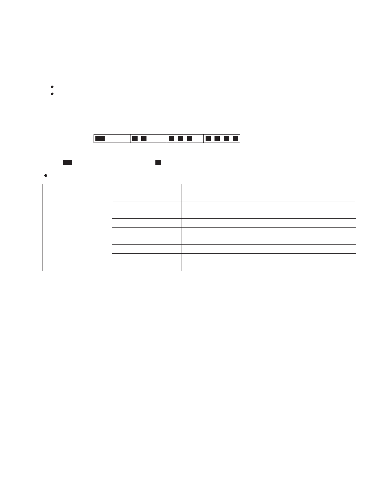
Table of errors classified by beep sounds
Diagnosis Beep signal sound Error message
Main board
(Note) A beep sound is also issued in case of other I/O trouble.
1(long sound)-2 BIOS ROM error
1-2-2-3
1-3-1-1
1-3-1-3
1-3-4-1
1-3-4-3
1-4-1-1
= short sound (about 0.2 sec.), Length between sounds is about 0.1 sec.
BIOS ROM error
RAM error
Keyboard controller error
RAM error
RAM error
RAM error
BIOS ROM error2-1-2-3
Occurrence of unexpected offering2-2-3-1
2-1

3. List of Error Codes <Only when the port replicator is connected>
The following is a list of the messages that BIOS can display. Most of them occur during POST.
Some of them display information about a hardware device, e.g., the amount of memory
installed. Others may indicate a problem with a device, such as the way it has been configured.
Following the list are explanations of the messages and remedies for reported problems.
If your system displays one of except the messages marked below with an asterisk (*), write
down the message and contact Panasonic Technical Support. If your system fails after you make
changes in the Setup menus, reset the computer, enter Setup and install Setup defaults or correct
the error.
0200 Failure Fixed Disk
Fixed disk in not working or not configured properly. Check to see if fixed disk is attached
properly. Run Setup. Find out if the fixed-disk type is correctly identified.
0210 Stuck key
Stuck key on keyboard.
0211 Keyboard error
Keyboard not working.
0212 Keyboard Controller Failed
Keyboard controller failed test. May require replacing keyboard controller.
0213 Keyboard locked - Unlock key switch
Unlock the system to proceed.
0230 System RAM Failed at offset: nnnn
System RAM failed at offset nnnn of in the 64k block at which the error was detected.
0231 Shadow RAM Failed at offset: nnnn
Shadow RAM failed at offset nnnn of the 64k block at which the error was detected.
0232 Extended RAM Failed at offset: nnnn
Extended memory not working or not configured properly at offset nnnn.
0250 System battery is dead - Replace and run SETUP
The CMOS clock battery indicator shows the battery is dead. Replace the battery and run
Setup to reconfigure the system.
*0251 System CMOS checksum bad - Default configuration used
System CMOS has been corrupted or modified incorrectly, perhaps by an application
program that changes data stored in CMOS. The BIOS installed Default SETUP Values.
If you do not want these values, enter Setup and enter your own values. If the error persists,
check the system battery or contact Panasonic Technical Support.
0260 System timer error
The timer test failed. Requires repair of system board.
0270 Real time clock error
Real-time clock fails BIOS test. May require board repair.
*0280 Previous boot incomplete - Default configuration used
Previous POST did not complete successfully. POST loads default values and offers to run
Setup. If the failure was caused by incorrect values and they are not corrected, the next boot
will likely fail. On systems with control of wait states, improper Setup settings can also
terminate POST and cause this error on the next boot. Run Setup and verify that the
wait-state configuration is correct. This error is cleared the next time the system is booted.
0281 Memory Size found by POST differed from EISA CMOS
Memory size found by POST differed from EISA CMOS.
3-1

02D0 System cache error - Cache disabled
Contact Panasonic Technical Support.
02F0: CPU ID:
CPU socket number for Multi-Processor error.
02F4: EISA CMOS not writable
ServerBIOS2 test error: Cannot write to EISA CMOS.
02F5: DMA Test Failed
ServerBIOS2 test error: Cannot write to extended DMA (Direct Memory Access) registers.
02F6: Software NMI Failed
ServerBIOS2 test error: Cannot generate software NMI (Non-Maskable Interrupt).
02F7: Fail - Safe Timer NMI Failed
ServerBIOS2 test error: Fail-Safe Timer takes too long.
device address Conflict
Address conflict for specified device.
Allocation Error for: device
Run ISA or EISA Configuration Utility to resolve resource conflict for the specified device.
Failing Bits: nnnn
The hex number nnnn is a map of the bits at the RAM address which failed the memory test.
Each 1 (one) in the map indicates a failed bit. See error 230,231 or 232 for offset address of
the failure in System, Extended or Shadow memory.
Invalid System Configuration Data
Problem with NVRAM (CMOS) data.
I/O device IRQ conflict
I/O device IRQ conflict error.
Operating System not found
Operating system cannot be located on either drive A: or drive C: Enter Setup and see if
fixed disk and drive A: are properly identified.
Parity Check 1 nnnn
Parity error found in the system bus. BIOS attempts to locate the address and display it on
the screen. If it cannot locate the address, it displays ????. Parity is a method for checking
errors in binary data. A parity error indicates that some data has been corrupted.
Parity Check 2 nnnn
Parity error found in the I/O bus. BIOS attempts to locate the address and display it on the
screen. If it cannot locate the address, it displays ????.
Press <F1> to resume, <F2> to Setup
Displayed after any recoverable error message. Press <F1> to start the boot process or <F2>
to enter a Setup and change the settings. Write down and follow the information shown on
the screen.
3-2

4. Diagnostic Test
4.1 Equipment
(1) Test Computer ································································································ 1 unit
(2) AC Adapter ····································································································· 1 pc.
(3) External Printer ······························································································· 1 unit
(4) Loopback Plug (Parallel Port Test) [ P/N: DFWV95C0081 ] ··························· 1 pc.
(5) Loopback Plug (Serial Port Test for RS232C) [ P/N: DFWV95C0067 ] ········· 1 pc.
(6) Floppy Disk containg file DIAG ······································································· 1 pc.
4.2 Preparation
(1) Connect the AC Adapter and External Printer to the computer.
(2) The System Setup should be set to the factory setting values by executing the “SETUP
UTILITY” which can be invoked by F2 key at the POST.
If not, the messages and items of the diagnostic test may not be displayed properly on the
LCD.
(3) The serial port must be enabled in the “SETUP UTILITY” in order to execute the “1st SERIAL
PORT” test.
(4) Connect the serial loopback plug.
(5) In order to test the parallel port with Loopback Plug, disconnect the printer cable and connect
the parallel loopback plug with Power OFF.
4.3 NOTICE
When “Enter password” is displayed, use “Password Skipping Plug” in order to skip the user
password.
1) Connect the parallel plug to the parallel port.
2) Connect the PS/2 mouse plug to the mouse port
3) Power on the computer.
The wiring of the parallel plug is described below.
Connect pins 2-5-6-8-11-13-15-18-19-20-21-22-23 to Shield GND (PS/2 mouse plug pin3).
Connect pins 3-4-7-9-10-12 to VC5 (PS/2 mouse plug pin4) with 4.7KW each.
CAUTION
The plug described above must be used for servicing purpose only.
Do not use it for other than the above purpose and ensure that it remains confidential.
Using the plug enables the user to skip the previous password and disable the password.
4-1

5 Self Diagnosis Test
1. Floppy disk is included for the self-diagnostic tests that should be performed before using this product.
2. Connect External Floppy Disk Drive (FDD) to USB port for diagnosis test.
Important notice
System password
This product has a password function. If this function is turned on, the self-diagnostics tests will not work.
You will need ask the user for the password before performing the self-diagnostics.
5.1. Outline of Self Diagnostic Tests
Insert the diagnostics floppy disk
Starting up the setup utility
Turn on the power.
When "Panasonic Press F2 to enter setup" appears
on the screen, press F2.
Return the setup
contents to default
Press " " to select [ Exit ]
Press " " to select [ Get default value ]
Press Enter.
Choose Yes for "Load default Configuration now?"
Select "Save Values & Exit" and press Enter.
Choose Yes for "Save Configuration changes and exit now?"
and press Enter.
Choose test from
the menu screen
to start the test.
Caution:
After completing repairs, be sure
to carry out the Automatic test
and Peripheraltest.
<Automatic test>
Tests selected (O) from the test
item list will be performed in
succession.
1. DIAG on FD
Menu Screen
1. DIAG on FD
2. LAN test
3. Modem test
4. Wireless LAN test (Wireless LAN Model only)
5. CD test
Q. Quit
<Peripheral test>
The parallel devices can be tested.
2. LAN test
3. Modem test
4. Wireless LAN test
(Wireless LAN Model only)
5. CD test
<Test selection>
Specifc tests required can
be freely selected and
performed from the test item
list.
Be sure to carry out the Selection
test only when necessary.
Problems in the unit are located and divided according
to error messages that occur during testing.
5-1
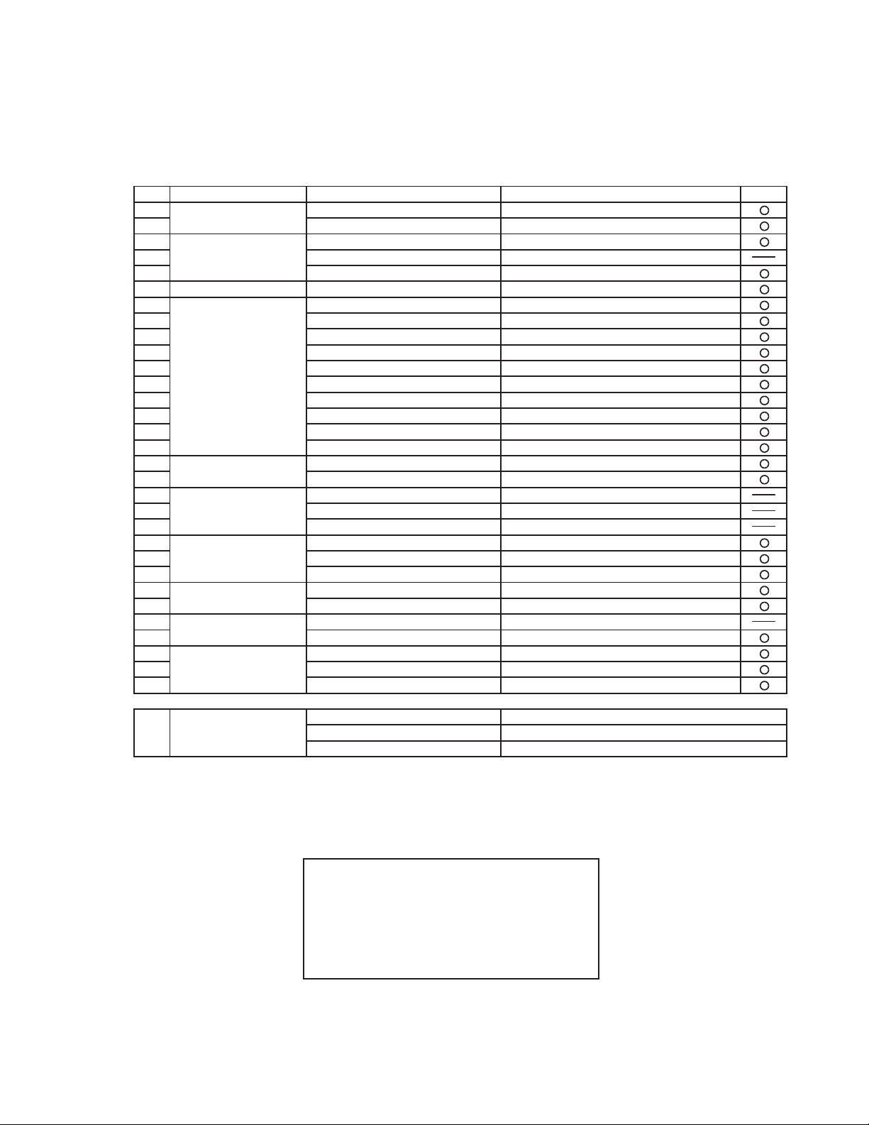
5.1.1. List of main test items
The selection item displays the items selected under Automatic test. If you select Automatic test, these test items
will be performed automatically. You can use Selection test to choose items from the menu screen that you want
to have tested.
These items are shown below.
1
2
CPU
3
(CPU related)
4
5
RAM (Memory related)
6
CONTROL
7
(Control ICs on the main
8
board, etc.)
9
10
11
12
13
14
15
16
IO
17
(Input-output)
18
COMMUNICATION
19
20
21
AUX
22
(Auxiliary functions)
23
24
VIDEO
25
(Display related)
26
DISK
27
(FDD, HDD)
28
UNIQUE
29
(Individual functions)
30
31
Test items shown on the screen Select
SPEAKER TEST Speaker test
VESA MODE TEST VESA mode test
A20 GATE TEST Address A20 line
CACHE ON/OFF TEST Cache memory on/off test
NPU OPERAND TEST Floating point processor function test
RAM STANDARD TEST Memory standard test
DMA PAGE REG TEST DMA page register test
DMA REGISTER TEST DAM register test
DMAC TRANSFER TEST DAM transfer test
PIC HALT INSTRUCTION TEST Interrupt controller halt instruction test
PIC REGISTER TEST Interrupt controller register test
RTC CMOS RAM TEST Real time clock CMOS test
RTC TEST Real time clock test
PIT CH0 TEST interrupt timer CH0
PIT CH1 TEST interrupt timer CH1
PIT CH2 TEST interrupt timer CH2
KEYBOARD REG TEST Keyboard test
PS/2 MOUSE REG Mouse registration test
SERIAL WRAP TEST Serial loop back (jig required)
SERIAL ALL INTERNAL TEST Serial port interior test
PARALLEL REGISTER R/W Parallel register R/W test
PCIC ALL TEST PCIC test
Card Bus Reg Card Bus register test
USB Reg USB register test
VGA ALL TEST VGA test
SVGA RAM TEST SVGA RAM test
FD WT/RD/WP TEST FD WT, RD WP test
HDD ALL TEST Only HDD lead test selected
ECP REGISTER R/W ECP register R/W test
EPP REGISTER R/W EPP register R/W test
EXT. CMOS R/W TEST Extension CMOS R/W test
ContentsTest classification
Test function settings
5.2. Automatic Test
Test execution
From the menu screen shown below For Celeron models Select and press Enter for DIAG on FD
Test condition save/play
Test automatic execute
Error display (Paging style)
Following file command
Test executed on run settings by selecting command
Select displayed items Error, Log, Option
1. DIAG on FD
2. LAN test
3. Modem test
4. Wireless LAN test (Wireless LAN Model only)
5. CD testQ. Quit
menu screen
5-2
Speaker test, VESA test
The speaker test involves listening to music and choosing OK or Not okay. The VESA test involves looking at
the display to see if it is satisfactory then choosing OK or Not okay.
Serial loop back test
The Automatic test’s initial settings are set so that the serial loop back test will be executed. Connect the serial
loop back jig and then perform the test.
(This test is not executed on default mode)
Diagnostics result
If no errors occur. The screen shows the word "Pass" in large letters.
If errors occur. The test is stopped when an error occurs and the error message is displayed.
For explanations of error messages, see Error Messages and Problem Categories (section 5.5).
Quitting the test
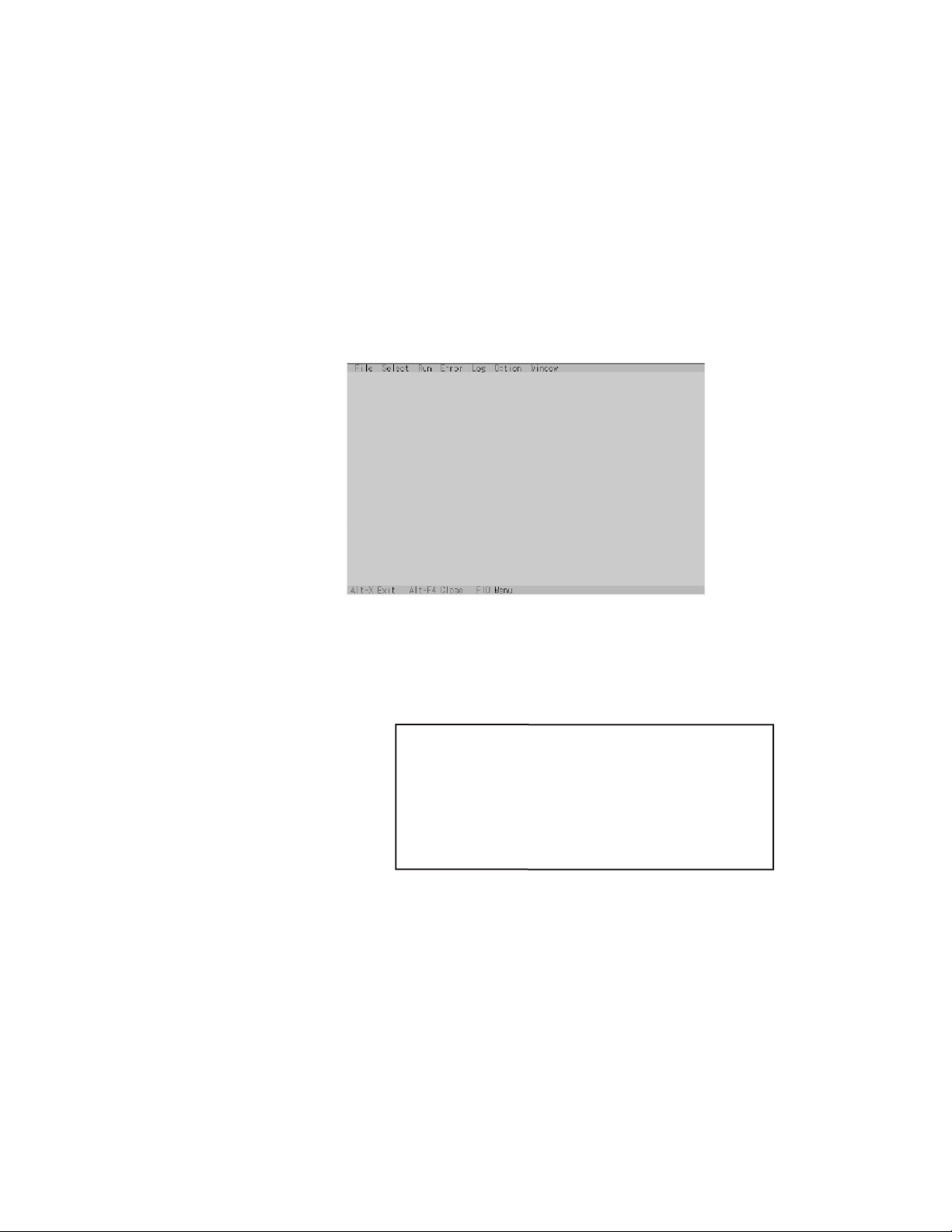
At the screen shown below, simultaneously press the ALT and X keys.
5.3. Peripheral Test
Test execution
From the menu screen shown below, be sure to choose the following items and press Enter.
2. LAN Test
This test checks for internal LAN device. Choose LAN test and press Enter.
3. Modem Test
4. Wireless LAN Test
5. CD Test
Input screen
1. DIAG on FD
2. LAN test
3. Modem Test
4. Wireless LAN test (Wireless LAN Model only)
5. CD test
Q. Quit
menu screen
5-3
5.4. Test Selection
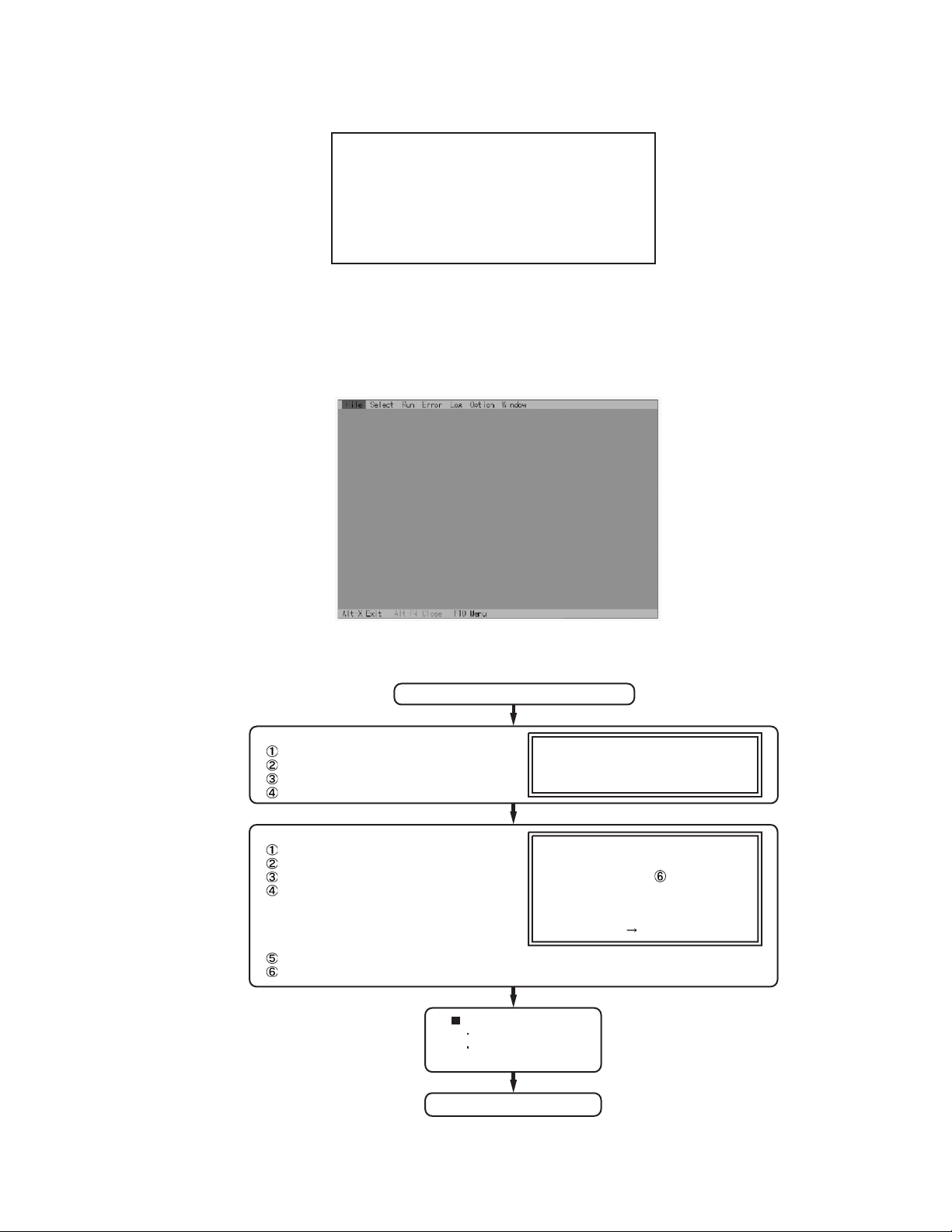
Starting up the input menu
1. From the menu screen shown below, choose Quit and press Enter.
2. When A: \DIAG appears, input "JDG_295, XEX" and press Enter.
3. The input screen shown below will appear.
To choose menu items, hold down "ALT" and press the selection key.
Example:
"ALT" + F brings up the File menu.
1. DIAG on FD
2. LAN test
3. Modem test
4. Wireless LAN test (Wireless LAN Model only)
5. CD testQ. Quit
menu screen
Order of test flow selection
1. Reading the test conditions settings file
Press "ALT" and "F".
Press "L".
Press "ALT" and "O".
Press Enter.
2. setting the test items
Press "ALT" and "S".
Press "S".
Choose the test item and press Enter.
Choose the test whose settings are-
to be changed, press "A" for Additional and "R" for Erase.
All initial VAlues are "0" so set
tests other than the necessary ones to "1".
Press "O" twice to return the menu screen.
To save the selected list, press "ALT" and "F" at the file menu.
Input screen
Input screen startup
If the test condition settings
file is not read, this means
the test program is not running correctly
[ Saving selected test items ]
If you change the file name when
saving the file in step
create test condition settings for
custom test items.
Example:
CF-29.
Starting the test
Press "ALT" and "R".
Press "R".
This will start the test.
* * *
, you can
TEST1.
.
* * *
End of test
5-4
5.5. Error Messages and Troubleshooting
The table below explains the parts that may be faulty or damaged should an error message occur while performing the
various test items of the self diagnostics program.
Test classification Screen display test items Contents
CPU
1
(CPU related)
2
3
4 RAM (Memory related)
CONTROL
5
(Control ICs on the
6
main board, etc.)
7
8
9
10
11
12
13
14
15
IO
16
(Input-output)
17
COMMUNICATION
18
19
20
AUX
21
(Auxiliary functions)
VIDEO
22
(Display related)
23
24
DISK
25
(FDD, HDD)
26
27
UNIQUE
(Individual functions)
28
29
A20 GATE TEST Address 20 line
CACHE ON/OFF Cache memory on/off
NPU OPERAND TEST Floating point processor function
RAM STANDARD Memory standard
DMA PAGE REG TEST DMA page register
DMA REGISTER TEST DAM register
DMAC Transfer TEST DAM transfer test
PIC HALT INSTRUCTION TEST Interrupt controller
PIC REGISTER TEST Interrupt controller
RTC CMOS RAM TEST Real time clock CMOS
SPEAKER TEST Speaker
PIT CH0 TEST Interrupt timer CH0
PIT CH1 TEST Interrupt timer CH1
PIT CH2 TEST Interrupt timer CH2
KEYBOARD REG TEST Keyboard
PS/2 MOUSE REG Mouse
SERIAL WRAP TEST Serial loop back (jig required)
SERIAL ALL INTERNAL TEST Serial port
PARALLEL REGISTER R/W Parallel register
PCIC ALL TEST PCIC
Card Bus REG Card Bus port
USB REG USB port
VGA ALL TEST VGA
SVGA RAM TEST SVGA RAM
VESA MODE TEST VESA mode
FD WT/RD/WP TEST FD write/read/write protection
HDD ALL TEST Only HDD lead selected
ECP REGISTER R/W Parallel port
EPP REGISTER R/W Parallel port
EXT. CMOS R/W TEST Extension CMOS R/W test
5-4

6 Wiring Connection Diagram
CN1
CN48
CN8
CN12
CN4
CN47
CN30
CN32
CN9
MAINP PCB
CN6
CN1
CN15
JK3
CN55
JK1
JK2
CN51
J1
J5
J6
CN2
CN1
W-LAN MODULE
KBD PCB
CN932
CN10
CN933
CN930
CN950
(FRONT SIDE)
CN952
(REVERSE SIDE)
LED PCB
CN980
TP PCB
EXT ANT.
PCB
CN801
CN800
CN803
IO PCB
KEYBOARD
ANTENNA
PCB
CN704 CN703
CN700
CN702
J1
J2
MDC MODEM
MODEM
PORT
DC-IN
USB
PORT
LAN PORT
PCMCIA
MAIN
BUTTERY
HDD
TOUCH PAD
ANTENNA
PCB
SPEAKER
HEADPHON
MIC
USB
PORT
RTC
BATTERY
CN1 CN2
INVERTER PCB
BACK LIGHT
LCD
CN56
SD PCB
CN2
CN13
PORT-REPLICATOR
SERIAL PORT PARALLEL PORT EXTERNAL DISPLAY PORT
6-1

7 Disassembly/Reassembly
Note:
Power off the computer. Do not shut down to the Suspend or hibernation mode.
Do not add peripherals while the computer is in the Suspend or hibernation mode; abnormal operation may result.
7.1. Disassembly Instructions
7.1.1. Preparation
Before disassembling, be sure to make the following preparations.
• Shut down Windows and turn off the power.
• Disconnect the AC adaptor.
• Remove the optional DIMM memory card and PCMCIA card
if they are connected.
• Remove other devices if they are connected.
Attention:
• Please execute writing BIOS ID when you exchange the
Main Board.
• You cannot reuse the Conductive Clothes and the heat dissipating parts such as Sheet and Rubber. Use new parts.
7.1.2. Removing the Battery Pack, HDD
Pack and FDD Pack
MP
Cover
1. Open the Battery Cover.
2. Remove the Battery Pack.
3. Open the HDD Cover.
4. Remove the HDD Pack.
5. Open the FDD Cover.
6. Remove the FDD Pack.
Use the MP Eject Lever.
7.1.3. Removing the HDD
HDD FPC
HDD
Heater Sheet
Sheet
Heater
Sheet
<A>
HDD U Case Ass’y
<A>
HDD
Damper
Ass’y
Ta b
HDD Case
Ass’y
Battery
Cover
Battery Pack
FDD Pack
MP RELEASE
HDD Pack
HDD Cover
Ta b
1. Remove the four Screws<A>.
2. Release the two Tabs, and remove the HDD U Case
Ass’y and the HDD L Case Ass’y.
3. Remove the HDD Damper Ass’y.
4. Remove the two Sheets.
5. Remove the Heater and the Heater Sheet.
6. Remove the HDD FPC.
Screws <A>: DFHE5025XA
Figure 1
7-1
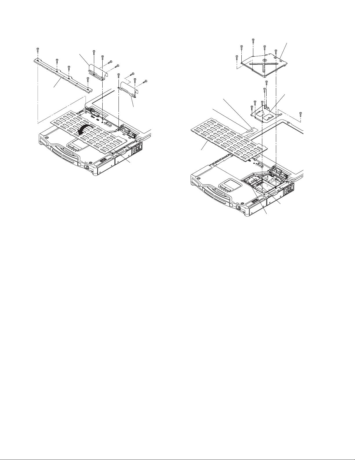
7.1.4. Removing the KB Cover, Hinge
Cover L, Hinge Cover R and Keyboard
<B>
Hinge Cover L
<B>
<B>
KB Cover
1. Remove the four Screws<B>, and remove the KB Cover.
2. Remove the four Screws<C> and the four Screws<D>,
and remove Hinge Cover L,R.
3. Remove the Keyboard.
Screws <B>: DRQT26+D4FZL
Screws <C>: DFHE5054XA
Screws <D>: DFHE5054XA
<B>
<D>
Figure 3
<D>
<C>
<C>
<D>
<C>
<D>
<C>
Hinge Cover R
Keyboard
7.1.5. Remove the KB Cable Cover,
Keyboard and PCMCIA Protector
<F>
<F>
<F>
<G>
<G>
<G>
Figure 4
<G>
<G>
Connector
(CN932)
to Connector
(CN933)
to Connector
(CN932)
Keyboard
1. Remove the five Screws<F>, and remove the KB Cable
Cover.
2. Disconnect the two Cables from two Connectors (CN932,
CN933)
3. Remove the six Screws<G>, and remove the PCMCIA
Protector.
<F>
KB Cable Cover
<F>
PCMCIA
Protector
Connector
(CN933)
<G>
Screws <F>: DRHM0002ZA
Screws <G>: DRQT2+I35FKL
7-2

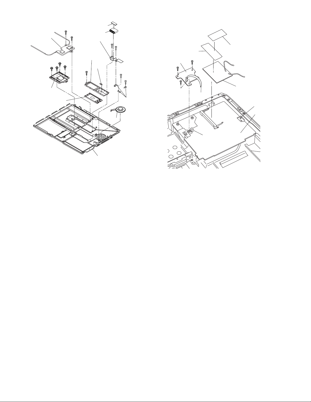
7.1.6. Removing the KBD PCB, MDC
Modem and LCD Cable/MIC Frame
7.1.7. Removing the DIMM Cover and
Bottom Cover
Connector J1
(reverse side)
<I>
<I>
Connector J2
(reverse side)
to Connector
(CN950)
to Connector
(CN952)
to Connector
(J2)
MDC
Modem
LCD Cable/
MIC Frame
KBD PCB
Connector CN950
(front side)
<H>
<H>
to Connector
(CN930)
Connector CN952
(reverse side)
Connector CN930
(reverse side)
Figure 5
1. Remove the LCD Cable/MIC Frame.
2. Remove the two Screws. <H>
3. Disconnect the three Cable from three Connectors
(CN930, CN950, CN952).
4. Remove the KB PCB.
5. Remove the two Screws. <I>
6. Disconnect the Cable from Connector. (J2)
7. Remove the MDC Modem.
DIMM Cover
DIMM Radiation
sheet
<K>
<L>
<L>
Bottom Cover
Connector CN12
<L>
<K>
<J>
<K>
<J>
<L>
<J>
<L>
<K>
<J>
<L>
<K>
<K>
to Connector
(CN12)
<L>
<K>
<L>
<K>
Screws <H>: DFHE5025XA
Screws <I>: DFHE5025XA
Figure 6
1. Remove the four Screws<J>, and remove the DIMM
Cover.
2. Remove the eight Screws<K> and the eight Screws<L>.
3. Disconnect the Cable from Connector (CN12).
Screws <J>: DRQT26+D4FZLT
Screws <K>: DRQT26+D4FZLT
Screws <L>: DRSB3+8FKL
7-3
7.1.8. Removing the Speaker
LCD Lamp Sheet
Coil Cooling Sheet
<N>
LAN Heat
Plate
MP Eject
BOUSUI
Plate
<P>
MP Eject
Spring
Bottom Cover
Heat Pipe Unit
Bottom
<O>
MP Eject
Lever
MP Eject Slide
Ass’y
<O>
<O>
<N>
<O>
<M>
Speaker
<M>
<M>
<M>
Speaker
Angle
7.1.9. Removing the Wireless Module and
SD PCB
MINI PCI Protector
Sheet
<Q>
SD PCB
<Q>
<Q>
to Connector
(CN56)
Connector CN???
CD Edge Sheet
to Connector
(CN2)
to Connector
(CN952)
Wireless Module
Connector CN2
Main PCB
Figure 7
1. Remove the LCD Lamp
2. Remove the four Screws<M>, and remove the LAN Heat
Plate, Speaker Angle and the Speaker.
3. Remove the two Screws<N>, and remove the Heat Pipe
Unit Bottom.
4. Remove the four Screws<O>, and remove the MP Eject
Lever.
5. Remove the Screw<P>, and remove the MP Eject
BOUSUI Plate and MP Eject Slide Ass’y.
Screws <M>: DXQT26+D4NLT
Screws <N>: DXYN+J6FNL
Screws <O>: DXYN26+F5NLT
Screw <P>: DXQT26+D4NLT
Figure 8
1. Disconnect the Cable from Connector (CN2).
2. Remove the Wireless Module.
3. Remove the MINI PCI Protector Sheet and the CD Edge
Sheet.
4. Remove the three Screws<Q>.
5.Disconnect the Cable from Connector (CN56).
6. Remove the SD PCB.
Screws <Q>: DFHE5025XA
7-4

7.1.10. Removing the PAD SW FFC Cover
<R>
<R>
PAD SW FFC
Cover
<R>
Power Cable
Guard
7.1.11. Removing Main PCB, EXT Antenna
PCB, PCMCIA Unit and RTC Battery
EXT Antenna PCB
Connector CN51
(front side)
<T-2>
Main PCB
<T-2>
<T-2>
<S>
<T-2>
<T-1>
<S>
Connector
CN1
Connector CN6
(reverse side)
Connector CN9
(reverse side)
Figure 9
1. Remove the three Screws<R>, and remove the PAD SW
FFC Cover.
Screws <R>: DFHE5054XA
Connector CN54
(reverse side)
Connector CN4
(reverse side)
PCMCIA Unit
to Connector
(CN4)
to Connector
(CN950)
<X>
<X>
RTC Battery
to Connector
(CN51)
<W>
Connector CN1
(reverse side)
to Connector
(CN9)
Connector CN10
(front side)
to Connector
(EXT Antenna CN1)
to Connector
(CN6)
<T-1>
<U>
<U>
<V>
<V>
<V>
to Connector
(CN54)
to Connector
(CN10)
to Connector
(Main PCB CN1)
Figure 10
1. Remove the two Screws<S>.
2. Remove the two Screws<T-1>.
3. Remove the two Screws<U>.
4. Remove the four Screws<V>.
5. Remove the Screw<W>.
6. Remove the two Screws<X>.
7. Disconnect the six Cables from six Connectors.
(Main PCB: CN1, CN6, CN9, CN10, CN51, CN54)
(EXT Antenna: CN1)
8. Remove the EXT Antenna.
9. Remove the Main PCB.
10. Disconnect the Cable from Connector (CN4).
11. Remove the RTC Battery
12. Remove the four Screws<T-2>, and remove the PCMCIA
Unit.
7-5

Screws <S>: DFHM5054XA
Screws <T-1>:DFHE5025XA
Screws <T-2>:DFHE5025XA
Screws <U>: DRQT2+G6FKL
Screw <V>: DRHM5104ZA
Screw <W>: DFHE5025ZA
Screw <X>: DRHM5117ZA
7.1.13. Removing the TP PCB
<c>
Connector CN801
Connector CN800
<c>
TP PBC
7.1.12. Remove the HDD Main FPC
CN Spacer
<a>
<b>
<a>
<Y>
<Z>
HDD Connector
HDD Main
FPC
Battery Connector
Batt HDD
CN Angle
<b>
Connector CN803
to Connector
(CN801)
to Connector
(CN800)
to Connector
(CN803)
Figure 11
1. Disconnect the three cables from three Connectors.
(CN800, CN801, CN803)
2. Remove the two Screws<c>, and remove the TP PCB.
Screws <c>: DRHM0002ZA
1. Remove the Screws<Y>, and remove the Batt HDD CN
Angle.
2. Remove the Screw<Z>, the two Screws<a> and the two
Screws<b>.
3. Remove the HDD Main FPC.
Screw <Y>: DFHE5092ZA
Screw <Z>: DFHE5025ZA
Screws <a>: DRHM5104ZA
Screws <b>: DFHE5025XA
7.1.14. Removing the IO PCB
IO PCB
<d>
<d>
<d>
<d>
<d>
Figure 12
1. Remove the six Screws<d>, and remove the IO PCB.
<d>
Screws <d>: DFHE5058ZB
7-6

7.1.15. Removing the Palm Top Cover
Sheet, Palm Top Cover, Touch Pad
Adhesion Seat, Touch Pad, Touch
Pad SW Knob, LED PCB and SW
LED PCB
Palm Top Cover Sheet
<e>
<e>
<e>
<e>
LED PCB
<e>
Palm Top Cover
Touch Pad Adhesion Seat
Touch Pad
PW LED
PCB
Touch Pad SW Knob
PW LED Sheet
<f>
SW LED
PCB
7.1.16. Removing the Handle and Power
SW
<g>
Handle Base L
Power
SW
Handle
<g>
Handle Base R
Touch Pad
SW Knob In
Figure 14
1. Remove the Palm Top Cover Sheet.
2. Remove the five Screws<e>, and remove Palm Top
Cover.
3. Remove the Touch Pad Adhesion Seat.
4. Remove the Touch Pad.
5. Remove the Touch Pad SW Knob and Touch Pad SW
Knob In.
6. Remove the LED PCB.
7. Remove the PW LED Sheet.
8. Remove the Screw<f>, and remove the SW LCD PCB.
Screws <e>: DRHM0002ZA
Screw <f>: DRHM0002ZA
Figure 15
1. Remove the two Screws<g>, and remove Handle Base
L,R.
2. Remove the Handle.
3. Remove the Power SW.
Screws <g>: DRSB4+8FKL
7-7
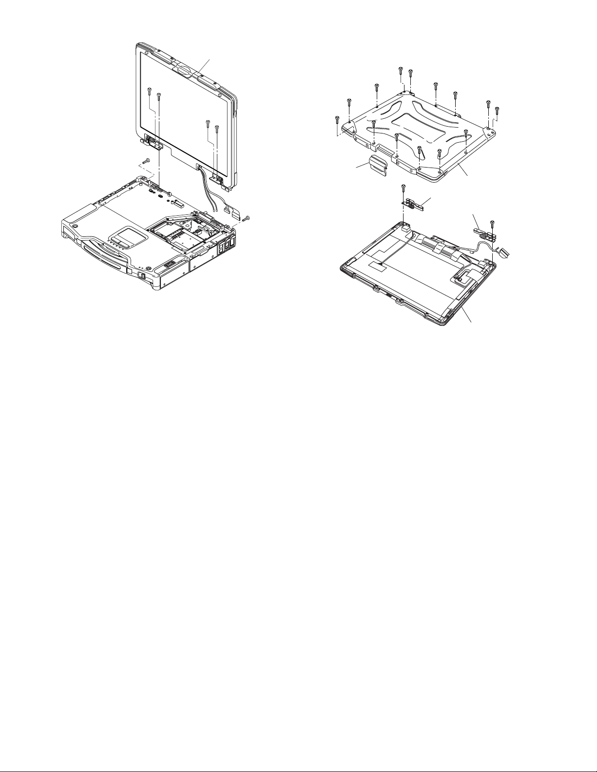
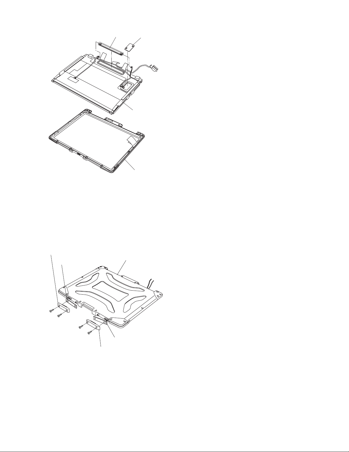
7.1.17. Removing LCD Unit
LCD unit
<i>
<i>
<i>
<i>
<h>
<h>
Figure 16
1. Remove the two Screws<h> and the four Screws<i>, and
remove the LCD Unit.
Screws <h>: DXSB4+12FNLB
Screws <i>: DXYN4+J8FNL
7.1.18. Removing LCD Rear Cabinet, Hinge
L and Hinge R
<k>
<j>
<k>
Hinge L
Figure 17
<k>
<k>
<k>
LCD Rear Cabinet
Hinge R
<j>
<k>
<k>
<l>
LCD Front Cabinet
<k>
<k>
<k>
LCD Latch
<k>
<k>
<l>
1. Remove the two Screws<j> and the twelve Screws<k>,
and remove the LCD Rear Cabinet.
2. Remove the LCD Latch.
3. Remove the two Screws<l>, and remove the Hinge L and
R.
Screws <j>: DRSB4+10FKL
Screws <k>: DRSB26+8HKL
Screws <l>: DRHM0062ZA
7-8
7.1.19. Removing the Inverter PCB, TS
PCB and LCD Unit
Inverter PCB
Figure 18
1. Disconnect two Cables from Connectors. (on Inverter
PCB)
2. Remove the Inverter PCB.
3. Disconnect two Cables from Connectors. (on TS PCB)
4. Remove the TS PCB.
5. Remove the LCD Unit.
TS PCB
LCD Unit
LCD Front Cabinet
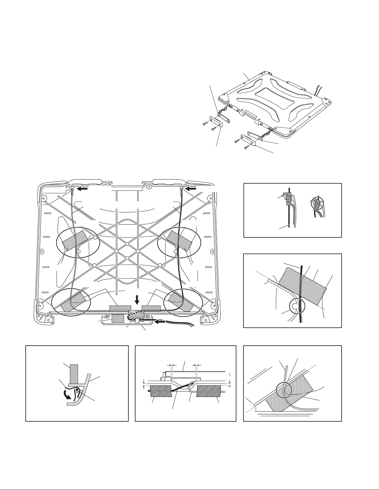
7.1.20. Removing the Antenna PCB L and
R
Antenna PCB Cover L
Antenna PCB L
<m>
<m>
<m>
<m>
1. Remove the four Screws<m>.
2. Remove the Antenna PCB Cover L and R and Antenna
PCB L and R.
Screws <m>:DRSB26+8KL
LCD Rear Cabinet Ass’y
Antenna PCB R
Antenna PCB Cover R
Figure 19
7-9
7.2. Reassembly Instructions
7.2.1.Attention when CF-29 series is repaired
• Please execute writing BIOS ID when you exchange the Main Board.
• You cannot reuse the Conductive Clothes and the heat dissipating parts such as Sheet and Rubber. Use new parts.
7.2.2. Setting the Antenna PCB L and R
1. Set the Antenna PCB L and R to the LCD Rear Cabinet
Ass’y.
2. Fix the Antenna PCB Cover L and R using the four
Screws. <i>
Screws <m>: DRSB26+8KL
n Arranging the Antenna L and R Cables
View "A"
Antenna Cable L Antenna Cable R
View "B"
View "B"
LCD Rear Cabinet Ass’y
Antenna PCB L
<m>
<m>
Antenna PCB
Cover L
View "A"
<m>
<m>
LCD Rear
Cabinet
Antenna
Cable
Antenna PCB R
Antenna PCB Cover R
View "A"
<No good>
Do not press too
much the
Waterproof Cap.
Ta pe Ta pe
Waterproof
Cushion
Cable Clamper
Bend
View "C" View "C"
View "D"
Cushion
Waterproof Cushion
Ta peTa pe
View "E"
Cable Clamper
View "E" View "D"
LCD Rear Cabinet
1~5mm
LCD Rear
Cabinet
Antenna Cable
L and R
Antenna Cable R
Antenna Cable L
1~5mm
View "B"
Antenna Cable R
Pass the Antenna
Cable through this
space.
Ta pe
align
View "C"
Pass the Antenna Cable
Antenna Cable L
1~4mm1~4mm
Ta peTa pe
through this space.
align
Ta pe
7-10

7.2.3. Setting the Inverter PCB, TS PCB and LCD Unit
1. Set the LCD Unit to the LCD Front Cabinet in order.
2. Attach the Inverter PCB to the LCD Unit and connect the
two Cables to the two Connectors on the Inverter PCB.
3. Attach the TS PCB to the LCD Unit in order and connect
the two Cables to the two Connectors on the TS PCB.
Safty Working
3
LCD Unit
View "A"
TS PCB
4
Inverter PCB
LCD Unit
n Attaching the Touch Screen Panel.
1. Attach the Touch Screen Panel to the LCD Front Cabinet using the TS Tape.
Note:
Use extreme caution when handling the Touch Screen Panel to avoid damage, fingerprints, etc.
View "A"
View "A"
Connectors
1
Touch Screen Panel
Connectors
TS PCB
View "A"
2
LCD Front Cabinet
TS FPC Spacer
Forming Unit
LCD Front Panel
3±1mm
View "B"
0±0.5mm
LID Magnet
TS FPC Spacer
TS FPC
TS Tape
TS FFC Sheet
View "B"
Forming Unit
LID Magnet
LCD Front Cabinet
0~1mm
7-11
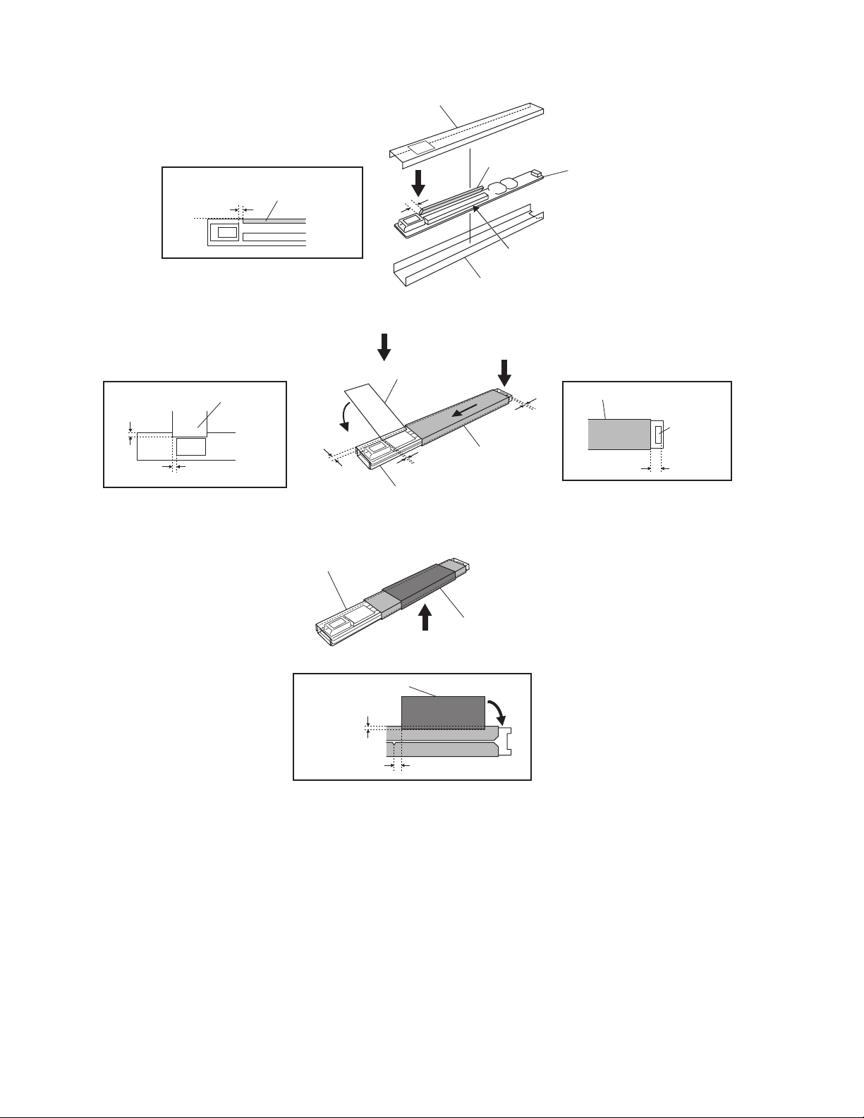
n Arranging the Inverter PCB
1. Attach the LCD Inverter Case Spacer L to the Inverter PCB.
2. Attach the Inverter Case L/U to the Inverter Case L.
Inverter Case U
LCD Inverter Case
Spacer L
Do not pressure to trance circuit.
Inverter Case L
Align
View "A"
1~2mm
LCD Inverter Case
Spacer L
View "A"
1~2mm
3. Attach the LCD Inverter Case Tape and the Inverter Shield to the Inverter Case.
View "B1"
View "B1"
LCD Inverter Case Tape
0~3mm
0~2mm
LCD Inverter Case Tape
0~3mm
0~2mm
Inverter Case
View "B2"
0~1mm
Inverter Shield
4. Attach the Inverter Shield Tape to the Inverter Case.
Inverter PCB
View "B2"
Inverter Shield
Connector
0~1mm
Inverter Case
Inverter Shield Tape
0~1mm
Inverter Shield Tape
View "C"
View "C"
0~2mm
7-12
 Loading...