

Panasonic AN8497SA Datasheet
ICs for Compact Disc/CD-ROM Player
AN8497SA
3-channel linear input PWM driver IC
■ Overview
The AN8497SA is a PWM output 3-channel
driver IC supporting linear inputs, and best suited for
an actuator and a motor drive for CD-ROM and
DVD-ROM. Due to its linear input, a conventional
system can be used only by replacing a driver. And,
due to an adoption of PWM output, you can reduce
considerably power consumption compared with a
conventional driver. Further a space saving surface
mount package is adopted thanks to its low thermal
generation.
■ Features
• Maximum 64% reduction of power consumption
compared with a conventional linear 3-channel
driver IC
• Free gain setting by an external resistor due to
voltage feedback
• Standby function available (standby current < 20 µA)
• Only for supply voltage 5 V
• Phase compensation function
■ Applications
• Optical disk drive
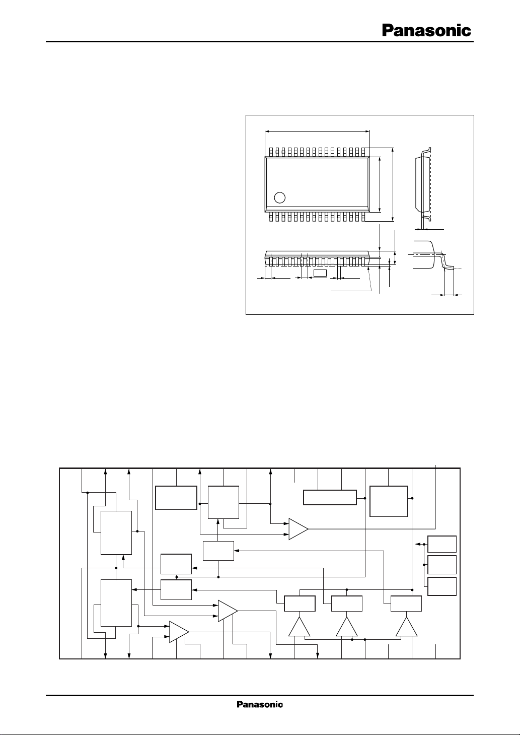
11.0±0.3
32
116
(0.625)
0.65
17
6.1±0.3
0.65±0.100.65±0.10
+0.10
0.3
–0.05
Seating plane
SSOP032 P-0300
8.1±0.3
1.5±0.2
0.1±0.1
Unit: mm
+0.10
0.2
–0.05
(0.5)
■ Block Diagram
PG12
FO2
32
31
H
bridge
H
bridge
1
2
FO1
VM12
30
3
RO2
RO1
SO2
29
Standby
(full circuit)
Pre-
driver
Pre-
driver
V/I
4
SO1
SB
28
5
YC1A
FO3
27
6
YC1B
bridge
Pre-
driver
PG3
26
H
V/I
7
YC2A
VM3
25
8
YC2B
RO3
N.C.
BC1
BC2
24
23
22
21
20
Charge pump
V/I
Logic Logic Logic
ABS ABS ABS
9
10
11
12
13
FB1
In1
FB2
In2
VPUMP
CLK
19
Triangular
wave
oscillator
14
REF
V
SGND
18
15
CT
In3
FB3
17
TSD
V
REF
detection
SV
DD
detection
16
DD
SV
1
AN8497SA ICs for Compact Disc/CD-ROM Player
■ Pin Descriptions
Pin No. Symbol Description
1 VM12 Channel 1, 2 power supply
2 FO1 Channel 1 forward output pin
3 RO1 Channel 1 reverse output pin
4 SO1 Channel 1 feedback signal input pin
5 YC1A
6 YC1B
7 YC2A
8 YC2B
Channel 1 feedback gain adjustment pin A
Channel 1 feedback gain adjustment pin B
Channel 2 feedback gain adjustment pin A
Channel 2 feedback gain adjustment pin B
9 FB1 Channel 1 feedback signal output pin
10 In1 Channel 1 driver input pin
11 FB2 Channel 2 feedback signal output pin
12 In2 Channel 2 driver input pin
13 V
Reference voltage input pin
REF
14 SGND Control circuit ground
15 In3 Channel 3 driver input pin
16 SV
Control circuit power supply
DD
Pin No. Symbol Description
17 FB3 Channel 3 feedback signal output pin
18 CT Triangular wave output pin
19 CLK CLK synchronous pulse input pin
20 VPUMP Charge pump step-up voltage output
21 BC2 Charge pump capacitor connection pin 2
22 BC1 Charge pump capacitor connection pin 1
23 N.C. N.C.
24 RO3 Channel 3 reverse output pin
25 VM3 Channel 3 power supply
26 PG3 Channel 3 power ground
27 FO3 Channel 3 forward output pin
28 SB All shut off input pin
29 SO2 Channel 2 feedback signal input pin
30 RO2 Channel 2 reverse output pin
31 FO2 Channel 2 forward output pin
32 PG12 Channel 1, 2 power supply
■ Absolute Maximum Ratings
Parameter Symbol Rating Unit
2
Supply voltage
Supply voltage application range SV
Drive output voltage
Control signal input voltage
Supply current
Drive output current channel 1, 2
Drive output current channel 3
Power dissipation
Operating ambient temperature
Storage temperature
Note) Do not apply external currents or voltages to any pins not specifically mentioned expect for the power supply and GND pins.
For circuit currents, '+' denotes current flowing into the IC, and '−' denotes current flowing out of the IC.
1: Except for the operating ambient temperature and storage temperature, all ratings are for Ta = 25°C.
*
2: The voltage in a step-up voltage circuit exceeds a supply voltage. Refer to "■ Electrical Characteristics" for an allowable
*
3: Use within 1 000 mA in each channel 1 and channel 2.
*
*
7
*
*
3
*
4
*
1
*
value of a step-up voltage.
SV
DD
V
, V
M12
M3
DD
V
, V
M12
M3
V
(m)
8
6
*
1
*
V
(n)
I
SVDD
I
VM12
I
VM3
5
*
I
(o)
I
(p)
P
D
T
opr
T
stg
6.0 V
− 0.3 to +6.0 V
7.0 V
SGND to SV
DD
200 mA
2 000
1 200
±1 000 mA
±1 200 mA
400 mW
−30 to +75 °C
−55 to +150 °C
V
2
 Loading...