

Panasonic AN8495SB Service Manual
New
0.30
+
0.10
-
0.05
21 152228
81471
0.65
±0.20
(1.315)
10.93
±0.30
8.30
±0.20
18.40
±0.20
(4.80)
(5.15)
SEATING PLANE
0.10
±0.10
2.70
±0.20
SEATING PLANE
(6.40)
(1.20)
0.35
+0.10
-
0.05
0˚ to 10˚
0.80
Stepping Motor Drive IC AN8495SB
■ Overview
AN8495SB is a stepping-motor-driving IC, created by using a D-MOS
process, and provides a maximum output of 30V at 1.5A. By the PWM drive
and 2-bit constant-current-chopping-drive method, the winding 1-2 phase
drive is possible.
■ Features
● 4-phase input (W1-2 phase excitation )
● 2-bit current level switching.
● Built-in noise canceler.
● Built-in phase-change thru-current protection function.
● Built-in flywheel diode
■ Applications
● Printer ● FAX ● PPC
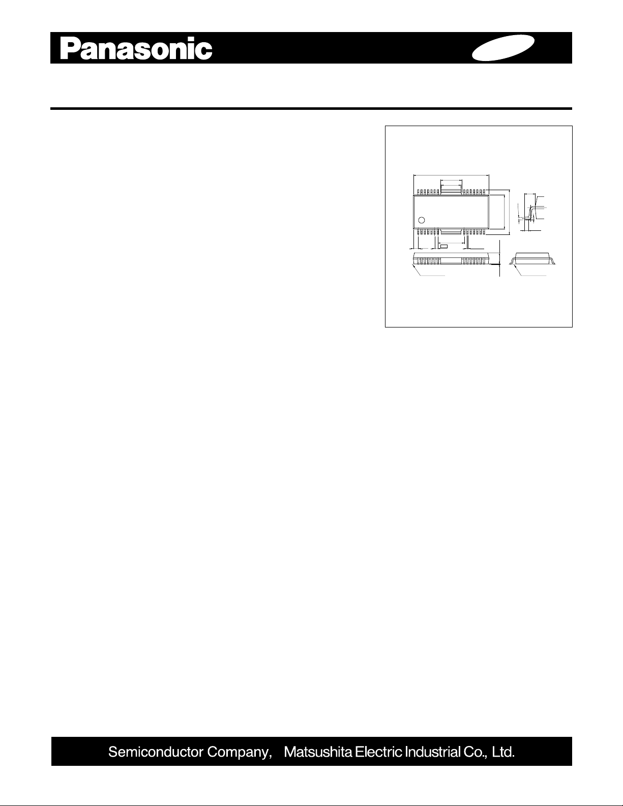
Unit:mm
HSOP042-P-0400
¶ The products and specifications are subject to change without any notice. Please ask for the latest product standards to guarantee the satisfaction of your product requirements.
1 Kotari Yakemachi, Nagaokakyo, Kyoto, 617-8520 Japan Tel. (075) 951-8151 http://www.panasonic.co.jp/semicon/
E00094AE
New publication, effective from Sep. 7. 2001
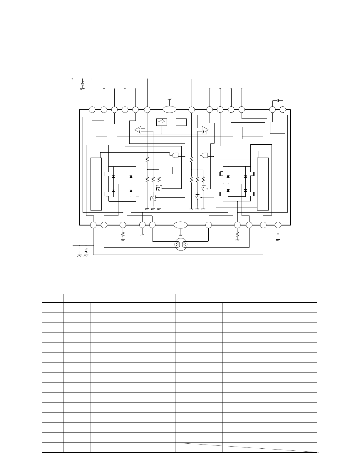
■ Block Diagram
V
CC
PHA1 IN0 IN1 IN2 IN3
ENABLEA
ENABLEB
PHB1
VM
25
* A voltage is applied externally to Terminals PHA1, PHB1, IN0 to 3, ENABLEA, ENABLEB, VREFA and VREFV, and may cause an overcurrent.
To protect the device from overcurrent, insert an overcurrent protective resistor (1KΩ or over).
1
7
GATE CIRCUIT
17 128 22
3
R
Q
S
16
Rs
4
Senser
Current
23
26
FIN
BLANK
ENA.off
Vref
TSD
Signal
15
OSC
FIN
24
Senser
Current
Vref
6
5
14 13
9
R
S
2
Q
Rs
20 19
CHARGE
PUMP
CIRCUIT
GATE CIRCUIT
21
■ Pin Description
Pin No. Function Pin No. Function
1 PHA1 A phase changeover terminal 16 RCSA A phase current detector
2 PHB1 B phase changeover terminal 17 AOUT1 Motor drive A phase output 1
3 IN0 A phase output torque control 1 18 N.C
4 IN1 A phase output torque control 2 19 BC1 Capacitor for charge pump circuit 1
5 IN2 B phase output torque control 1 20 BC2 Capacitor for charge pump circuit 2
6 IN3 B phase output torque control 2 21 VPUMP Charge pump circuit output
7
8 VM1 Supply terminal for Motor 1 23 VREFA A phase torque ref. voltage input
9
10 N.C 25 VCC Supply terminal
11 N.C 26 GND Signal GND
12 BOUT2 Motor drive B phase output 2 27 N.C
13 RCSB B phase current detector 28 N.C
14 BOUT1 Motor drive B phase output 1 FIN GND Signal GND
15 AOUT2 Motor drive A phase output 2
ENABLEA
ENABLEB
A phase start/stop signal input 22 VM2 Supply terminal for Motor 2
B phase start/stop signal input 24 VREFB B phase torque ref. voltage input

■ Absolute Maximum Ratings
Parameter
Storage temperature
Operating ambient temperature
Supply voltage
Supply current
Power dissipation
Motor supply voltage
Output voltage
Motor drive current
Flyhoile diode current
Charge pump circuit voltage
Symbol
T
T
opr
V
CC
I
CC
P
VM1/V
V
OUT
I
OUT
I
V
PUMP
Rating
stg
-55 to +150
-20 to +70
7.0
30
D
M2
1.04
30
30
±1.5
f
1.5
40
Note 1) Ta=25°C except storage temperature and operating ambient temperature.
Note 2) Power dissipation shows the value of only package at Ta=70°C.
■ Recommended Operating Range
Operating supply voltage range
V
CC
V
M
4.75 V to 5.25 V
18.0 V to 28.0 V
Unit
°C
°C
V
mA
W
V
V
A
A
V
Note
1
1
2
Pin=8,22
Pin=12,14
15,17
Pin=21
■ Electrical Characteristics (Ta = 25 °C ± 2 °C,VCC =5.0 V,VM = 24 V )
Parameter Symbol Condition min typ max Unit
Power block
Output saturation voltage H V
Output saturation voltage L V
Flywheel diode forward voltage V
Output leak current 1 I
LEAK1
Circuit current
Supply current (2-circuit ON) I
I/O block
IN “H” input voltage V
IN “L” input voltage V
IN “H” input current I
IN “L” input current I
PHA1,PHB1 “H” input voltage V
PHA1,PHB1 “L” input voltage V
PHA1,PHB1 “H” input current I
PHA1,PHB1 “L” input current I
PHAH/PHBH
PHAL/PHBL
PHAH/PHBH
PHAL/PHBL
OH
OL
CC
INH
INL
INH
INL
DI
ENABLEA=ENABLEB= 0 V 5 9.5 mA
I = -1.0 A VM-0.75 VM-0.5 V
I = 1.0 A 0.65 0.98 V
I = 1.0 A 0.5 1.0 1.5 V
V
OUT
= 30 V,V
= 0 V 10 50 µA
RCS
VIN = 5 V -10 0 10 µA
VIN = 0 V -80 -40 -20 µA
PHA1 = PHB1 = 5 V -10 0 10 µA
PHA1 = PHB1 = 0 V -150 -100 -50 µA
2.0 V
CC
GND 0.6 V
2.0 V
CC
GND 0.6 V
V
V
 Loading...