

ICs for Compact Disc/ CD-ROM Player
AN8488SB
3-phase full-wave motor driver and DC motor BTL driver IC
■ Overview
The AN8488SB is a motor driver IC incorporating a 3-phase full-wave motor driver and DC motor
BTL driver IC with a reverse rotation brake/short
brake changeover function. It is encapsulated into a
high allowable power dissipation package (with copper block).
■ Features
• 3-phase full-wave and snubberless
• FG output
• Current limit
• Reverse rotation prevention
• Thermal protection circuit built-in
■ Applications
• Various types of optical disk drive
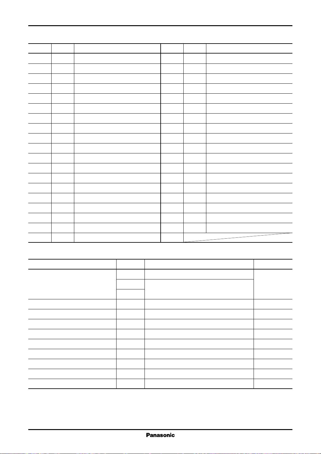
■ Block Diagram
SG
FIN1
changeover
Direction
detection
ER
Logic
EP = ER × EA
Absolute
value
Direction
VTL
H1+
H1−
H2+
H2−
H3+
H3−
VH
EC
ECR
16
17
18
19
20
21
23
27
26
Hall
amp.
matrix
Detection
Hall
bias
EA
Start/stop
(1.20)
Upper side
distribution
Lower side
distribution
Thermal
protection
circuit
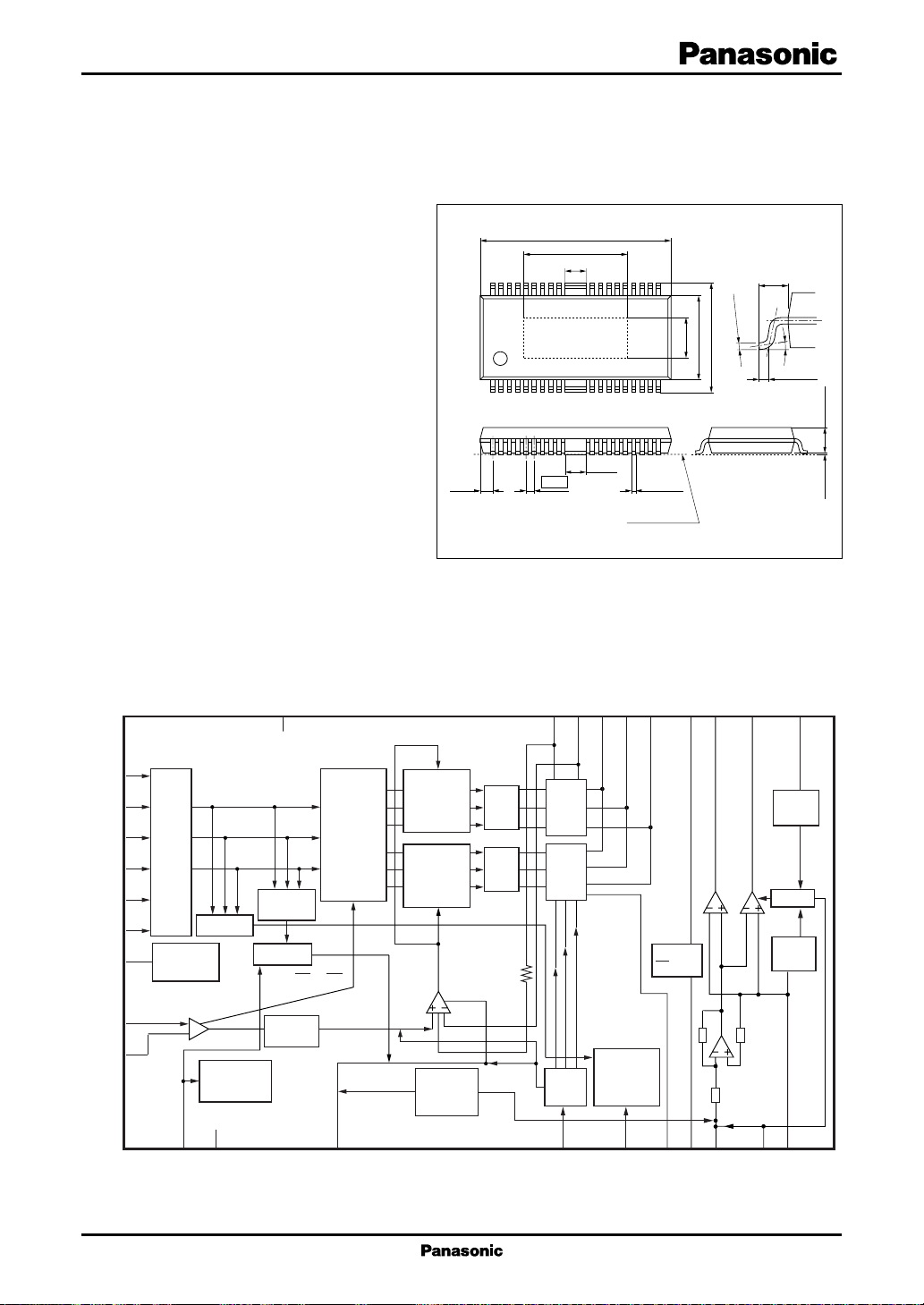
18.4±0.2
(10.00)
0.80
(1.95)
(3.20)
0.35
Seating plane
42 34 30 22
1 9 13 21
HSOP042-P-0400C
VM1CSA1A2A3
32
35
36
34
29
Upper
Amp.
Amp.
side
power
Lower
side
power
Brake
circuit
FG
comparator
1
2
+0.10
– 0.05
(4.00)
9
VM2
Unit: mm
(1.315)
– 0.05
+0.10
0.30
8.3±0.2
10.93±0.30
VM2VNVP
7
4
0° to 10°
0.5±0.2
V
CC2
det
Reset
V
REF
det.
10
V
.
2.7±0.20.1±0.1
CC2
25
S/S
22
CC1
V
28
PCI
15
BRK
14121
FG
PG1
2
PG2
11
SLIN
5
PC
REF
V
1
AN8488SB ICs for Compact Disc/ CD-ROM Player
■ Pin Descriptions
Pin No. Symbol Description
1 PG1 SPD block power GND pin
2 PG2 Driver block power GND pin
3 N.C. N.C.
4 VN Driver block inverted output pin
5 PC Driver block power cut pin
6 N.C. N.C.
7 VP Driver block forward output pin
8 N.C. N.C.
9 VM2 Driver block motor power supply pin
10 V
Driver block supply voltage pin
CC2
11 SLIN Driver block input pin
12 V
Driver block reference input pin
REF
13 N.C. N.C.
14 FG FG signal output pin
15 BRK Brake mode setting pin
16 H1+ Hall element-1 positive input pin
17 H1− Hall element-1 negative input pin
18 H2+ Hall element-2 positive input pin
FIN1 SG Signal GND pin
Pin No. Symbol Description
19 H2− Hall element-2 negative input pin
20 H3+ Hall element-3 positive input pin
21 H3− Hall element-3 negative input pin
22 V
SPD block supply voltage pin
CC1
23 VH Hall bias pin
24 N.C. N.C.
25 SS Start/stop changeover pin
26 ECR Torque command reference input pin
27 EC Torque command input pin
28 PCI
Current feedback phase compensation pin
29 VM1 SPD block motor supply voltage pin
30 N.C. N.C.
31 N.C. N.C.
32 A3 A3 phase output pin
33 N.C. N.C.
34 CS Current det. pin
35 A2 A2 phase output pin
36 A1 A1 phase output pin
FIN2
■ Absolute Maximum Ratings
Parameter Symbol Rating Unit
Supply voltage V
4
Output voltage 1
Output voltage 2
Control signal input voltage
*
5
*
4
*
Supply current I
3
Output current
*
Hall bias current I
2
Power dissipation
Operating ambient temperature
Storage temperature
Note) Do not apply external currents or voltages to any pins not specifically mentioned.
For circuit currents, '+' denotes current flowing into the IC, and '−' denotes current flowing out of the IC.
1: Except for the operating ambient temperature and storage temperature, all ratings are for Ta = 25°C.
*
2: The power dissipation shown is the value of independent IC without a heat sink at Ta = 75°C. Refer to the PD Ta curves
*
of the "■ Application Notes" for details.
*
1
*
1
*
CC1
V
CC2
VM1 , V
V
O1(n)
V
O2(n)
V
(n)
CC1
I
O(n)
HB
P
D
T
opr
T
stg
M2
7.0 V
14.0
− 0.3 to VM1 + 0.4 V
− 0.3 to VM2 + 0.4 V
0 to V
CC1
30 mA
±1 200 mA
50 mA
786 mW
−20 to +75 °C
−55 to +150 °C
V
2
ICs for Compact Disc/ CD-ROM Player AN8488SB
■ Absolute Maximum Ratings (continued)
Note)*3: n = 4, 7, 32, 35, 36
4: n = 32, 35, 36
*
5: n = 4, 7
*
6: n = 5, 11, 12, 15, 25, 26, 27
*
■ Recommended Operating Range
Parameter Symbol Range Unit
Supply voltage V
CC1
V
CC2
VM1 , V
■ Electrical Characteristics at Ta = 25°C
Parameter Symbol Conditions Min Typ Max Unit
Overall
Circuit current 1 I
Circuit current 2 I
Start/stop
Start voltage V
Stop voltage V
Medium voltage V
<Spindle block>
Hall bias
Hall bias voltage V
Hall amplifier
Input bias current I
In-phase input voltage range V
Minimum input level V
Torque command
In-phase input voltage range EC V
Offset voltage EC
Dead zone EC
Input current EC
Input/output gain A
Output
High-level output saturation voltage V
Low-level output saturation voltage V
Torque limit current I
CC1
CC2
START
STOP
MED
HB
BH
HBR
INH
OF
DZ
IN
CS
OH
OL
TL
M2
V
= 5 V, SS: at low 00.1mA
CC1
V
= 12 V, SS: at low 60 200 µA
CC2
Voltage with which a circuit operates 2.7 V
at V
= 5 V and L → H
CC1
Voltage with which a circuit becomes 0.7 V
off at V
= 5 V and H → L
CC1
Voltage with which V
low at V
V
CC1
V
CC1
V
CC1
V
CC1
CC1
V
CC1
V
CC1
V
CC1
V
CC1
V
CC1
V
CC1
= 5 V and EC = 0 V
CC1
= 5 V, IHB = 20 mA 0.7 1.2 1.6 V
= 5 V 15µA
= 5 V 1.5 4.0 V
= 5 V 60 mV[p-p]
= 5 V 0.5 3.9 V
= 5 V −100 0 100 mV
= 5 V 25 75 125 mV
= 5 V, EC = ECR = 1.65 V −5 − 0.25 µA
= 5 V, RCS = 0.6 Ω 0.75 1.0 1.25 A/V
= 5 V, IO = −300 mA 0.9 1.6 V
= 5 V, IO = 300 mA 0.2 0.6 V
VCC = 5 V, RCS = 0.6 Ω 400 500 600 mA
4.25 to 5.5 V
4.5 to 13.5
becomes 1.425 1.65 1.89 V
PC1
3
 Loading...