

Panasonic AN8480NSB Datasheet
ICs for Compact Disc/CD-ROM Player
AN8480NSB
3-phase full-wave motor driver IC
■ Overview
The AN8480NSB is a 3-phase full-wave motor
driver IC with a reverse rotation brake/short brake
changeover function, incorporating a thermal protection circuit with its protection monitor pin.
■ Features
• 3-phase full-wave and snubberless
• FG output
• Current limit
• Reverse rotation prevention
• Thermal protection circuit built-in (with thermal
protection monitor pin)
■ Applications
• Various types of optical disk drive
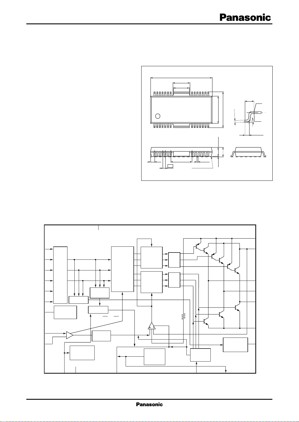
■ Block Diagram
SG
15
2
H1+
3
H1−
H2+
H2−
H3+
H3−
VH
EC
ECR
5
6
8
9
7
18
17
Hall
amp.
matrix
Hall
bias
10
S/S
Detection
EA
Start/stop
16
CC
V
Direction
detection
ER
Logic
EP = ER × ΕΑ
Absolute
value
Direction
changeover
20
PCI
28 22 21
17 814
(1.2)
Upper side
distribution
Lower side
distribution
VTL
Thermal
protection
circuit
0.8
Amp.
Amp.
18.4±0.2
(5.15)
(4.8)
(6.4)
HSOP042-P-0400
+0.10
0.35
–0.05
Seating plane
Brake
circuit
13
BRK
Unit: mm
15
(1.315)
–0.05
+0.10
8.3±0.22.7±0.20.1±0.1
10.93±0.30
0.30
FG
comparator
0° to 10°
0.65±0.20
21
VM
22
CS1
28
A1
27
A2
26
A3
1
PG
12
FG
11
TSDF
1

AN8480NSB ICs for Compact Disc/CD-ROM Player
■ Pin Descriptions
Pin No. Symbol Description
1 PG Power GND pin
2H1+ Hall element-1 positive input pin
3H1− Hall element-1 negative input pin
4 N.C. N.C.
5H2+ Hall element-2 positive input pin
6H2− Hall element-2 negative input pin
7 VH Hall bias pin
8H3+ Hall element-3 positive input pin
9H3− Hall element-3 negative input pin
10 SS Start/stop changeover pin
11 TFLG Thermal protection monitor pin
12 FG FG signal output pin
13 BRK Brake mode setting pin
14 N.C. N.C.
Pin No. Symbol Description
15 SG Signal GND pin
16 V
Supply voltage pin
CC
17 ECR Torque command reference input pin
18 EC Torque command input pin
19 N.C. N.C.
20 PCI
Current feedback phase compensation pin
21 VM Motor supply voltage pin
22 CS Current det. pin 1
23 N.C. N.C.
24 N.C. N.C.
25 N.C. N.C.
26 A3 Drive output 3
27 A2 Drive output 2
28 A1 Drive output 1
■ Absolute Maximum Ratings
Parameter Symbol Rating Unit
Supply voltage V
4
Control signal input voltage
*
Supply current I
3
Output current
*
Hall bias current I
2
Power dissipation
Operating ambient temperature
Storage temperature
Note) Do not apply external currents or voltages to any pins not specifically mentioned.
For circuit currents, '+' denotes current flowing into the IC, and '−' denotes current flowing out of the IC.
1: Except for the operating ambient temperature and storage temperature, all ratings are for Ta = 25°C.
*
2: For 70°C and IC alone.
*
3: n = 1, 22, 26, 27, 28
*
4: n = 2, 3, 5, 6, 8, 9, 10, 13, 17, 18
*
*
1
*
1
*
V
V
I
T
T
CC
O(n)
HB
P
CC
M
(n)
D
opr
stg
7.0 V
14.4
0 to V
CC
30 mA
±1 200 mA
50 mA
667 mW
−20 to +70 °C
−55 to +150 °C
■ Recommended Operating Range
Parameter Symbol Range Unit
Supply voltage V
CC
V
M
4.25 to 5.5 V
4.5 to 14
V
2
 Loading...