

Panasonic AN8473SA Datasheet
ICs for Compact Disc/CD-ROM Player
AN8473SA
Spindle motor driver IC for optical disk
■ Overview
The AN8473SA is an optical disk driver IC,
featuring direct PWM drive, DMOS power drive,
low ON resistance of output power MOS and 120°
of duty-factor.
■ Features
• RON = 0.5 Ω (for both upper and lower)
• 5 V single power source
• Circuit current 7 mA (including step-up circuit
current)
■ Applications
• Optical disk
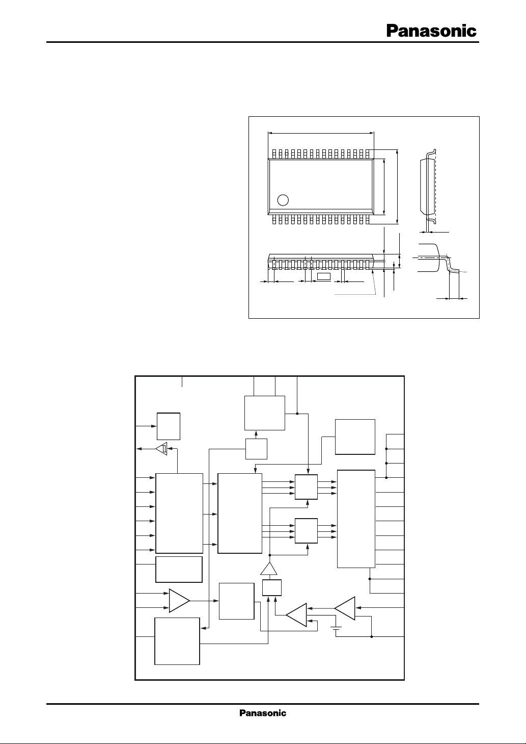
■ Block Diagram
DD
V
16
11
10
7
6
5
4
3
2
1
8
9
Start/
stop
Hall amp.
matrix
Hall
bias
Distributor
Absolute
Start
FG
H1H
H1L
H2H
H2L
H3H
H3L
VH
EC
ECR
circuit
value
11.0±0.3
32
116
0.65
VPUMP
12
14
BC2
(0.625)
BC1
13
17
6.1±0.3
0.65±0.100.65±0.10
+0.10
0.3
–0.05
Seating plane
SSOP032-P-0300
8.1±0.3
1.5±0.2
0.1±0.1
Step-up
voltage
circuit
OSC
Thermal
protection
17
18
32
31
Amp.
27
28
PWMOUTU
Amp.
Output
circuit
24
25
21
PWMOUTL
22
23
FF
× 5
26
19
VM21
VM22
VM11
VM12
A11
A12
A21
A22
A31
A32
PG2
PG1
CS
Unit: mm
+0.10
0.2
–0.05
(0.5)
PWMSW
30
changeover
PWM
frequency
circuit
SSET
V
T
SRESET
V
C1
15
GND
1
AN8473SA ICs for Compact Disc/CD-ROM Player
■ Pin Descriptions
Pin No. Symbol Description
1 VH Hall bias pin
2 H3L Hall element-3 negative input pin
3 H3H Hall element-3 positive input pin
4 H2L Hall element-2 negative input pin
5 H2H Hall element-2 positive input pin
6 H1L Hall element-1 negative input pin
7 H1H Hall element-1 positive input pin
8 EC Torque command input pin
9 ECR Torque command reference input pin
10 FG FG signal output pin
11 Start Start/stop changeover pin
12 VPUMP Booster pin
13 BC1 Booster capacitor connection pin 1
14 BC2 Booster capacitor connection pin 2
15 GND Ground pin
16 V
Supply voltage pin
DD
Pin No. Symbol Description
17 VM21 Motor supply voltage pin 2
18 VM22 Motor supply voltage pin 2
19 CS Current det. pin
20 N.C. N.C.
21 A31 Drive output 3
22 A32 Drive output 3
23 PG2 Power current det. pin 2
24 A21 Drive output 2
25 A22 Drive output 2
26 PG1 Power current det. pin 1
27 A11 Drive output 1
28 A12 Drive output 1
29 N.C. N.C.
30 PWMSW PWM frequency changeover pin
31 VM12 Motor supply voltage pin 1
32 VM11 Motor supply voltage pin 1
■ Absolute Maximum Ratings
Parameter Symbol Rating Unit
2
Supply voltage
Drive output voltage
Control signal input voltage
Supply current I
Drive output current
Hall bias current
Power dissipation
Operating ambient temperature
Storage temperature
Note) Do not apply external currents or voltages to any pins not specifically mentioned.
For circuit currents, '+' denotes current flowing into the IC, and '−' denotes current flowing out of the IC.
1: Except for the operating ambient temperature and storage temperature, all ratings are for Ta = 25°C.
*
2: The voltage in the step-up voltage circuit exceeds the supply voltage.
*
3: The power dissipation shown is the value of independent IC without a heat sink at Ta = 70°C. Refer to the PD Ta curves
*
4: o = 17, 18, 21, 22, 23, 24, 25, 26, 27, 28, 31, 32
*
6: n = 2, 3, 4, 5, 6, 7, 8, 9, 11, 30
*
*
5
*
6
*
4
*
7
*
3
*
1
*
1
*
For the allowable value of the step-up voltage, refer to "■ Electrical Characteristics".
of the "■ Application Notes" for details.
V
V
M11, 12
V
M21, 22
V
V
I
HB(n)
T
T
DD
(m)
(n)
DD
I
(o)
6.5 V
15 V
0 to V
DD
30 mA
±1 200 mA
30 mA
P
D
opr
stg
5: m = 21, 22, 24, 25, 27, 28
*
7: n = 1
*
293 mW
−30 to +85 °C
−55 to +150 °C
V
2
 Loading...