

Panasonic AN8470NSA Datasheet
ICs for Compact Disc/CD-ROM Player
AN8470NSA
Spindle motor driver IC for optical disk
■ Overview
The AN8470NSA is a high performance IC
suited for driving a spindle motor of an optical disk
such as CD-ROM, PD, DVD, CD-R, CD-RW, etc.
■ Features
• Low power consumption due to a direct PWM
system
• With start and stop pin
• Reverse breaking by EC/ECR voltage
• With Hall bias pin
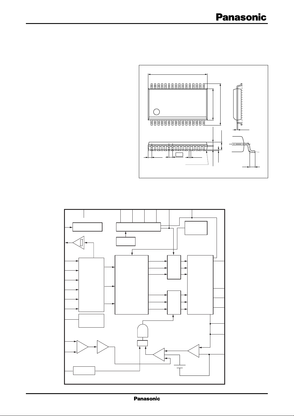
• Surface-mount small package
■ Applications
• High speed CD-ROM drive
PD, DVD, CD-R, CD-RW drives
■ Block Diagram
Start
FG
7
24
DD
V
9
Start/stop
BC411BC3
Step-up voltage circuit
OSC
12
11.0±0.3
32
116
0.65
VPUMP15VM1
13
BC2
(0.625)
BC1
14
17
6.1±0.3
0.65±0.100.65±0.10
+0.10
0.3
–0.05
Seating plane
SSOP032-P-0300
6
8.1±0.3
1.5±0.2
0.1±0.1
Thermal
protection
Unit: mm
+0.10
0.2
–0.05
(0.5)
H1H
H1L
H2H
H2L
H3H
H3L
VH
EC
ECR
FC
23
22
21
19
18
17
8
27
26
25
Hall amp.
matrix
Hall
bias
V
Oscillator
32
VM2
Amp.
Distributor
circuit
Amp.
PWMOUT
T
FF
PNFOUT
Output
circuit
× 5
31
30
10
3
1
2
A1
A2
A3
RNF2
RNF1
GND
SRESET
V
CL
SSET
1
AN8470NSA ICs for Compact Disc/CD-ROM Player
■ Pin Descriptions
Pin No. Symbol Description
1 A2 Drive output 2
2 RNF2 Current det. pin 2
3 A1 Drive output 1
4 N.C. N.C.
5 N.C. N.C.
6 VM1 Motor supply voltage pin 1
7 Start Start/stop changeover pin
8 VH Hall bias pin
9VDDSupply voltage pin
10 GND Ground pin
11 BC4 Booster capacitor connection pin 4
12 BC3 Booster capacitor connection pin 3
13 BC2 Booster capacitor connection pin 2
14 BC1 Booster capacitor connection pin 1
15 VPUMP Booster pin
16 N.C. N.C.
Pin No. Symbol Description
17 H3L Hall element-3 negative input pin
18 H3H Hall element-3 positive input pin
19 H2L Hall element-2 negative input pin
20 N.C. N.C.
21 H2H Hall element-2 positive input pin
22 H1L Hall element-1 negative input pin
23 H1H Hall element-1 positive input pin
24 FG FG signal output pin
25 FC Oscillator pin
26 ECR Torque command reference input pin
27 EC Torque command input pin
28 N.C. N.C.
29 N.C. N.C.
30 RNF1 Current det. pin 1
31 A3 Drive output 3
32 VM2 Motor supply voltage pin 2
■ Absolute Maximum Ratings
Parameter Symbol Rating Unit
2
Supply voltage
Drive output voltage
Control signal input voltage
Supply current I
Drive output current
Hall bias current I
Power dissipation
Operating ambient temperature
Storage temperature
Note) Do not apply external currents or voltages to any pins not specifically mentioned.
For circuit currents, '+' denotes current flowing into the IC, and '−' denotes current flowing out of the IC.
1: Except for the operating ambient temperature and storage temperature, all ratings are for Ta = 25°C.
*
2: The voltage in the step-up voltage circuit exceeds the supply voltage.
*
3: For 70°C and IC alone.
*
4: o = 1, 2, 3, 6, 30, 31, 32
*
5: m = 1, 3, 31
*
6: n = 7, 17, 18, 19, 21, 22, 23, 26, 27
*
*
5
*
6
*
4
*
3
*
1
*
1
*
For the allowable value of the step-up voltage, refer to "■ Electrical Characteristics".
V
DD
V
M1
V
M2
V
(m)
V
(n)
DD
I
(o)
HB
P
D
T
opr
T
stg
6.0 V
15.0 V
0 to V
DD
30.0 mA
±1 200 mA
30.0 mA
293 mW
−20 to +70 °C
−55 to +150 °C
V
2
ICs for Compact Disc/CD-ROM Player AN8470NSA
■ Recommended Operating Range
Parameter Symbol Range Unit
Supply voltage V
DD
V
M1
V
M2
■ Electrical Characteristics at Ta = 25°C
Parameter Symbol Conditions Min Typ Max Unit
Overall
Circuit current 1 I
Circuit current 2 I
Start/stop
Start voltage V
START
Stop voltage V
Hall bias
Hall bias voltage V
Hall amplifier
Input bias current I
In-phase input voltage range V
Minimum input level V
Torque command
In-phase input voltage range EC VDD = 5 V 0.5 3.9 V
Offset voltage EC
Dead zone EC
Input current EC
Input/output gain A
Output
High-level output saturation voltage V
Low-level output saturation voltage V
Torque limit current I
OSC
Charging current I
Upper threshold voltage V
Lower threshold voltage V
VDD = 5 V in power save mode 00.1mA
DD1
VDD = 5 V 914mA
DD2
Voltage with which a circuit operates 2.7 V
at VDD = 5 V and L → H
Voltage with which a circuit becomes 0.7 V
STOP
off at VDD = 5 V and H → L
VDD = 5 V, IHB = 20 mA 0.7 1.1 1.6 V
HB
VDD = 5 V 15µA
BH
VDD = 5 V, except for H2H, H2L 1.5 4.0 V
HBR
VDD = 5 V 60 mV[p-p]
INH
VDD = 5 V −100 0 100 mV
OF
VDD = 5 V 0 75 150 mV
DZ
VDD = 5 V, EC = ECR = 2.5 V −5 −1 µA
IN
VDD = 5 V, RCS = 0.33 Ω 0.36 0.48 0.60 A/V
CS
VDD = 5 V, IO = −500 mA 0.25 0.50 V
OH
VDD = 5 V, IO = 500 mA 0.25 0.50 V
OL
VDD = 5 V, RCS = 0.33 Ω 455 570 685 mA
TL
VDD = 5 V −65 −50 −35 µA
CH
VDD = 5 V 1.75 2.50 3.25 V
CH
VDD = 5 V 0.35 0.50 0.65 V
CL
4.5 to 5.5 V
3
 Loading...