

Panasonic AN8387S Datasheet
ICs for CD/CD-ROM Player
■ Overview
The AN8387S is an IC which incorporates 2 circuits of
BTL drivers for driving various DC motors such as actuators (focus, tracking traverse), spindles, and loading of
the CD players.
■ Features
•
Operating supply voltage range ; V
CC
=3.5V to 9V
PVCC=1.5V to 9V
•
Built-in 2 circuits of voltage driven BTL drivers
(maximun drive current : 500mA)
•
Quiescent current (current consumption at no input) ;
3.2mA
•
Provided with power control pin
•
Provided with driver output voltage limiting pin
•
Built-in thermal protective circuit
(operating temperature : 160°C typ.)
■ Applications
Linear driving of the DC motors and actuators of the
CD players. CD radio cassette tape recorders, and so
on.
AN8387S
2-channel Linear Driver
Unit : mm
0.1±0.1
2.05±0.2
(0.4)
1
2
3
4
5
6
7
8
9
10
20
19
18
17
16
15
14
13
12
11
0.4±0.25
1.27
12.63±0.3
5.5±0.3
7.6±0.3
(0.4)
0.9±0.25
0.2
+ 0.1
– 0.05
0.9±0.25
20-Lead SOP Package (SOP020-P-0300A)
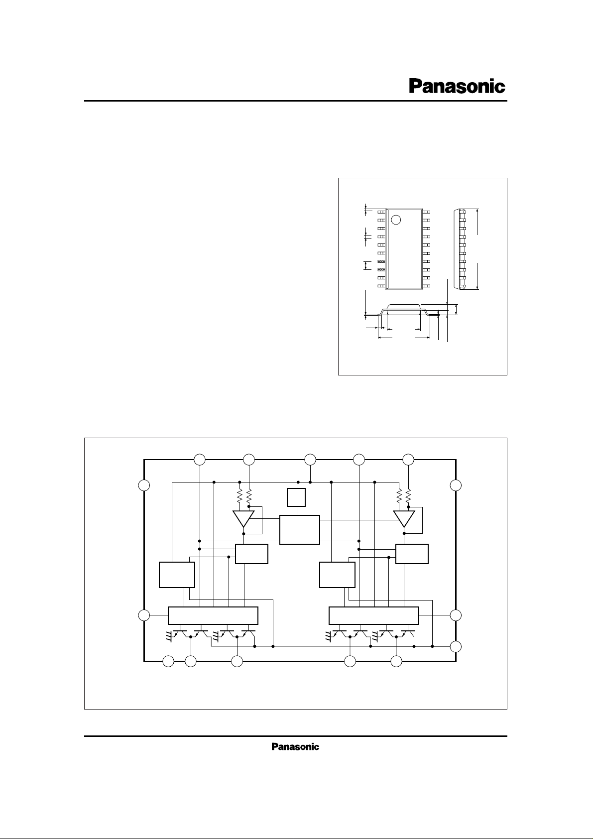
■ Block Diagram
8 9 4 3 2
7
GND
–+ –+
Absolute
Value
Base
Current
Control
11
c 14 13 17 18
P.GND
BTL
a) V
b) P.V
c) PGND : Pin5, Pin6, Pin15, Pin16
CC
CC
V
REF
SW
Thermal
Shutdown
: Pin1, Pin10
: Pin12, Pin19
Base Power
Control
10kΩ 1kΩ
BTL
Absolute
Value
a
V
CC
20
b
P.V
CC

ICs for CD/CD-ROM Player
AN8387S
V
CC
P
D
T
opr
T
stg
Supply Voltage
Power Dissipation
Operating Ambient Temperature
Storage Temperature
V
mW
˚C
˚C
Parameter Symbol Rating Unit
10
1,200
Note)
–30 ~ +85
–55 ~ +125
Note) When mounted onto the glass epoxy PCB (50mm × 50mm × 0.8mm)
■ Absolute Maximum Ratings (Ta=25˚C)
Parameter Symbol Range
Operating Supply Voltage Range
V
CC
P.V
CC
3.5V ~ 9V
1.5V ~ 9V
■ Recommended Operating Range (Ta=25˚C)
Current Consumption at No Input (VCC)
Current Consumption at No Input (PV
CC
)
PV
CC
Leak Current
V
ref
Threshold (H)
Note 1)
V
ref
Threshold (L)
Note 2)
Input Amp. Input Impedance
Driver Input Offset Voltage
Note 3)
Driver Output Offset Voltage
Note 3)
Driver Dead Zone Width
Note3)
Driver Transfer Gain (+)
Note3)
Driver (+), (–) Transfer Gain Ratio
Note 3)
Driver Output Voltage
Driver Output Voltage Absolute Value
Driver Power Transistor Saturation
Voltage
PC Input Pin Threshold Voltage (H)
Note 4)
PC Input Pin Threshold Voltage (L)
Note 5)
Protective Diode Forward Voltage
Thermal Protective Circuit Operating
Temperature
I
VCCQ
I
PVCCQ
I
PVCCL
V
refH
V
refL
RA
IN
V
I offset
V
O offset
|VDZ|
G
+
RG
V
OLG
|VOL|
V
sat
V
PC THH
V
PC THL
V
PD
T
THD
VCC=9V, V
ref
=4.5V, PVCC=9V
V
CC
=9V, V
ref
=4.5V, PVCC=9V
VCC=
0V, V
ref
=
OPEN, PVCC=
10V
VCC=3V, PVCC=10V, VIN=0V
V
CC
=3V, PVCC=10V, VIN=0V
V
CC
=9V, V
ref
=4.5V, PVCC=9V
V
CC
=9V, V
ref
=4.5V, PVCC=9V
V
CC
=9V, V
ref
=4.5V, PVCC=9V
V
CC
=9V, V
ref
=4.5V, PVCC=9V
V
CC
=9V, V
ref
=4.5V, PVCC=9V
1
0.7
1.45
0.75
–10
–55
–10
13
–1.9
–130
2.25
2.8
0.9
2
1.2
1
0
0
15.1
– 0.9
0.29
1.5
160
3.5
3.5
1
1
1.25
10
55
19
17
0.5
130
3
0.38
0.8
1.8
mA
mA
µA
V
V
kΩ
mV
mV
mV
dB
dB
mV
V
V
V
V
V
˚C
Parameter Symbol Condition min. typ. max. Unit
■ Electrical Characteristics (Ta=25˚C)
VCC=9V, V
ref
=4.5V, PVCC=9V,
V
LIM
=0V
I
O
=300mA
VCC=9V, V
ref
=4.5V, PVCC=9V,
V
LIM
=3V
V
CC
=9V, V
ref
=4.5V, PVCC=9V,
IO=300mA
V
CC
=9V, V
ref
=2.5V, PVCC=5V,
VIN=2.3V
V
CC
=9V, V
ref
=2.5V, PVCC=5V,
VIN=2.3V
V
CC
=5V, V
ref
=2.5V,
VIN=2.4→2.6V
Note1) V
ref
voltage required to operate the driver.
Note2) If V
ref
is made lower than this voltage, the driver dose not operate.
Note3) Refer to the driver input/output characteristics chart.
Note4) If the PC pin voltage is made higher than this voltage, there will be no output voltage from the driver. Both (+
) and (–)
outputs are pulling in the current.
Note5) If the PC pin voltage is made lower than this voltage, the driver operates normally.
 Loading...