

Panasonic AN8353UB Datasheet
■ Overview
The AN8353UB is a dimmer IC to control illumination of the
car dashboard at high efficiency and high performance by pulse
width control. It outputs pulses at a duty proprotional to an
input voltage.
■ Features
•
Low power consumption by pulse control
•
External ON/OFF control by the standby pin
•
Pulse frequency range : 50Hz to 10kHz
•
Built-in overvoltage protective circuit approx. 20V
•
Wide operating ambient temperature range : –40˚C to+100˚C
•
All products temperature cycle, high reliability by normal
and high temperature checks reliability equivalent to the air
bags requested in U.S.
AN8353UB
High Efficiency Car Dashboard Dimmer IC
9
8
7
6
5
4
3
2
0.3
+0.1
– 0.05
23.3±0.3
6.0±0.3
2.4±0.25
3.3±0.25
1.5±0.25
0.5±0.1
2.54
1.5±0.25
1.4±0.3
30˚
3.0±0.3
Unit : mm
1
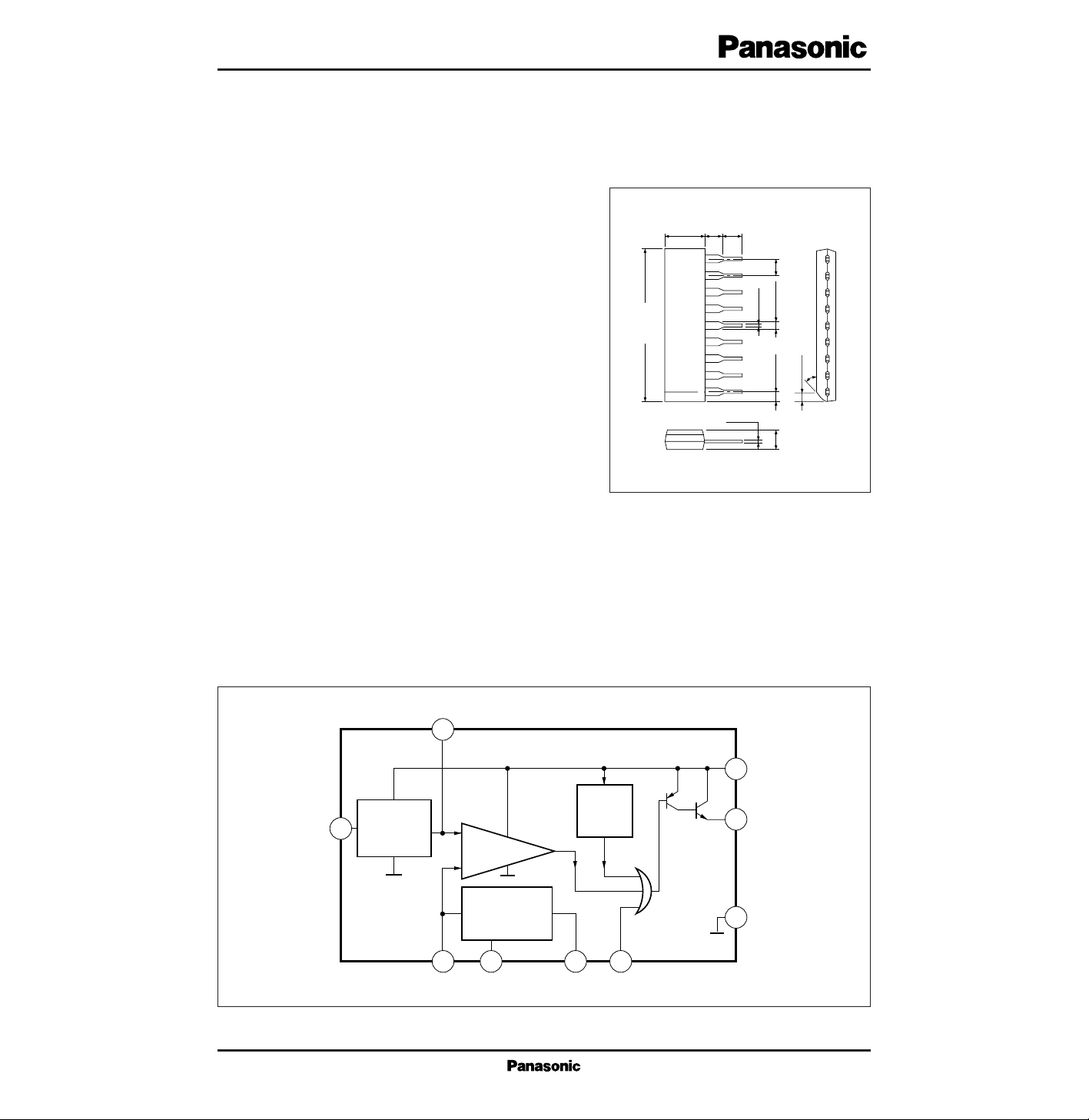
9-pin SIL Plastic Package (SIP009-P-0000C)
■ Block Diagram
3
Control
Voltage
Conversion
4
Over
Voltage
Protector
PWM
Comparator
Triangular
Wave Gen.
6 5 7 8
9
V
CC
1
GND
2
Pin No.
Pin name
■ Pin Descriptions
Description
1 Output pin
Outputs an intermittent source current at a duty proportional to an input voltage
2 GND GND
3 Input pin Applies a control voltage.
4
Noise eliminating capacity connection pin 1
Connect a capacitor to eliminator a noise.
7
Noise eliminating capacity connection pin 2
Connect a capacitor to eliminator a noise.
9 V
CC
Supply Voltage
5 Square wave output pin
6 Triangular wave output pin
8 Standby pin
Output a triangular wave, which serves as a reference for the PWM signal,
to the Pin6 by connecting the resistor R
T
between the Pins5 and6, and
capacity C
T
between the Pin6 and GND.
Output a triangular wave, which serves as a reference for the PWM signal,
to this pin by connecting the resistor R
T
between the Pins6 and 5, and
capasity C
T
between the Pin6 and GND.
Forces to shut off an output current if a voltage higher than a threshold
voltage of 1.1V is applied to the Pin8.
V
CC
P
D
T
opr
T
stg
Supply voltage
Power dissipation
Storage temperature
Operating ambient temperature
V
mW
˚C
˚C
Parameter Symbol Rating Unit
■ Absolute Maximum Ratings (Ta=25˚C)
22
550
–40 to +100
–50 to +150
Parameter Symbol Range
■ Recommended Operating Range (Ta=25˚C)
Operating supply voltage range
V
CC
8 to 18V
Parameter Symbol Condition min typ max
■ Electrical Characteristics (Ta=25˚C)
Supply current
I
CC
11 mA7.5
Eliminate C
T
and R
T
Oscillation frequency
f
osc
Hz115
C
T
=0.027µF
0% duty input voltage
V
IN – 0
3 V2.5
C
T
=0.027µF
100% duty input voltage
V
IN– 100
V
C
T
=0.027µF
Center duty (VCC=12V)
D
12V
%45
C
T
=0.027µF
%
C
T
=0.027µF
Center duty (VCC=8V)
DD
8V
%0
C
T
=0.027µF
10
Center duty (VCC=18V)
DD
18V
%50
C
T
=0.027µF
Output duty gain
D
G
V
Output voltage at ON
V
ON
µA0
C
T
=2100pF
Leakage current at OFF
I
L
V20
C
T
=2100pF
22
1.65
4
55
1.2
10.5
140
55
1
1
18
45
0.6
4
90
2
9.5
35
–1
–1
Over voltage detection voltage
V
OV
CT=2100pF
V1.1
CT=2100pF
Standby threshold voltage
V
STH
0
0.9
0.55
Unit
 Loading...