

Panasonic AN8261 Datasheet
■ Overview
The AN8261 is a 3-phase full-wave brushless motor drive IC
and optimum for driving the air conditioner fan motors, etc.
■ Features
•
Operating supply voltage range : VCC= 4.5 to 7V
•
3-phase full-wave drive, external power transistor
•
Built-in low-voltage protective circuit
•
Built-in thermal protective comparator circuit
•
Built-in Hall amplifiers with hysteresis
■ Applications
Driving the brushless motors such as air conditioner fan
motors, etc.
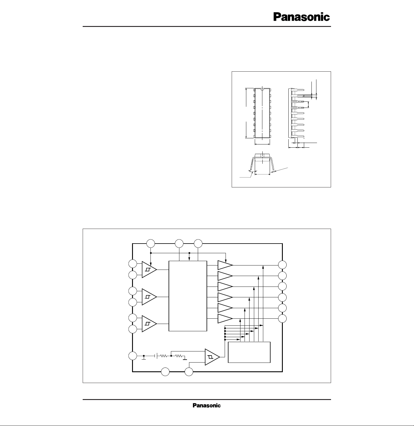
AN8261
Brushless Motor Driver
1
2
3
4
5
6
7
8
9
18
17
16
15
14
13
12
11
10
3.8
±0.25
(3.45)
1.2±0.25
0.5±0.1
2.54
Unit : mm
6.3±0.25
21.7±0.3
3 ~15˚
0.3
+0.1
– 0.25
7.62±0.25
18-pin DIL Plastic Package (DIP018-P-0300D)
0.51min.
■ Block Diagram
V
CC
1
18
17
Hysteresis Amp.A
16
15
Hysteresis Amp.B
14
GND
13
Hysteresis Amp.C
V
4
REF
2 3
Signal Processing
TSD Hysteresis Control
6 5
7
12
8
11
9
10
VCCMonitor
Protector
V
CC
Supply voltage
V
Parameter Symbol Rating Unit
■ Absolute Maximum Ratings (Ta=25˚C)
7.5
I
CC
Supply current
mA
80
I7, I8, I
9
I10, I11, I
12
Output drive current
mA
–7 to + 25
P
D
Power dissipation
mW
800
T
opr
Operating ambient temperature
˚C
–20 to + 80
T
stg
Storage temperature
˚C
–55 to +150
Parameter Symbol Range
■ Recommended Operating Range (Ta=25˚C)
Operating supply voltage range
V
CC
4.5V to 7V
Parameter Symbol Condition min typ max
■ Electrical Characteristics (Ta=25˚C)
Supply current 1
I
CC1
56 mA40
V
CC
=5V
Supply current 2
I
CC2
mA47
V
CC
=3.5V
Sensor amp. input voltage L to H
V
SLH
20 mV10
V
CC
=5V
Sensor amp. input voltage H to L
V
SHL
mV
V
CC
=5V
FG output voltage low level
V
OL
V
V
CC
=5V, IPO=5mA
V
V
CC
=5V, IPO=–3mA
Power drive output voltage high level
V
POH
mA–6
V
CC
=5V, VPO=2V
–10
Power drive output current high level
I
POH
V
V
CC
=5V, IPO=10mA
Power drive output voltage low level 1
V
POL1
V
Power drive output voltage low level 2
V
POL2
V
V
CC
=5V, IPO=20mA
Power drive output voltage low level 3
V
POL3
mV20
V
CC
=5V, IPO=15mA
28
12
4.5
0.6
0.4
0.6
–1
62
0.4
–4
12
1
–20
3.6
–8
Sensor amp. input voltage hysteresis width
V
SW
VCC=5V
kΩ10
I
W
=30µA
FG output pull-up resistance value
R
O
V4
Protect reset voltage
V
R
V1.15
Temperature protect operating voltage
V
T
V0.63
V
CC
=5V
0.8
1.3
0.5
1
8
3.5
Temperature protect resetting voltage
V
TR
VCC=5V
µA10
TSD bias current
I
TSD
VCC=5V, V
TSD
=0.5V
V2.3 2.62
Reference voltage
V
ref
VCC=5V
V0.15
Reference voltage regulation
V
refREGV
VCC=4V→7V
V0.1
Reference voltage load reguration
V
refREGV
VCC=5V, IO=0mA→10mA
mV210 450100
V
CC
protect hysteresis width
V
CCW
%50 51.548.5
Temperature protect operating voltage V
ref
ratio
VT/V
ref
VCC=5V
%27.4 29.525.3
Temperature protect operating voltage V
ref
ratio
VR/V
ref
VCC=5V
Unit
 Loading...