

Panasonic AN8140K Datasheet
1
A/D and D/A Converters
■ Overview
The AN8140K is a 10-bit D/A converter for image processing which has realized low power comsumption by
using the Bi-CMOS process.
■ Features
• 10-bit resolution
•
High speed : maximum conversion rate of 50MSPS
•
Low power comsumption : 150mW
•
TTL compatible input level
•
Single 5V power supply
•
Built-in reference power supply
■ Application Field
•
Image equipment such as hi-vision device
•
OA equipment such as image scanner
•
Measuring equipment such as digital oscilloscope
AN8140K
High-speed Low Power Consumption 10-bit D/A Converter
Unit : mm
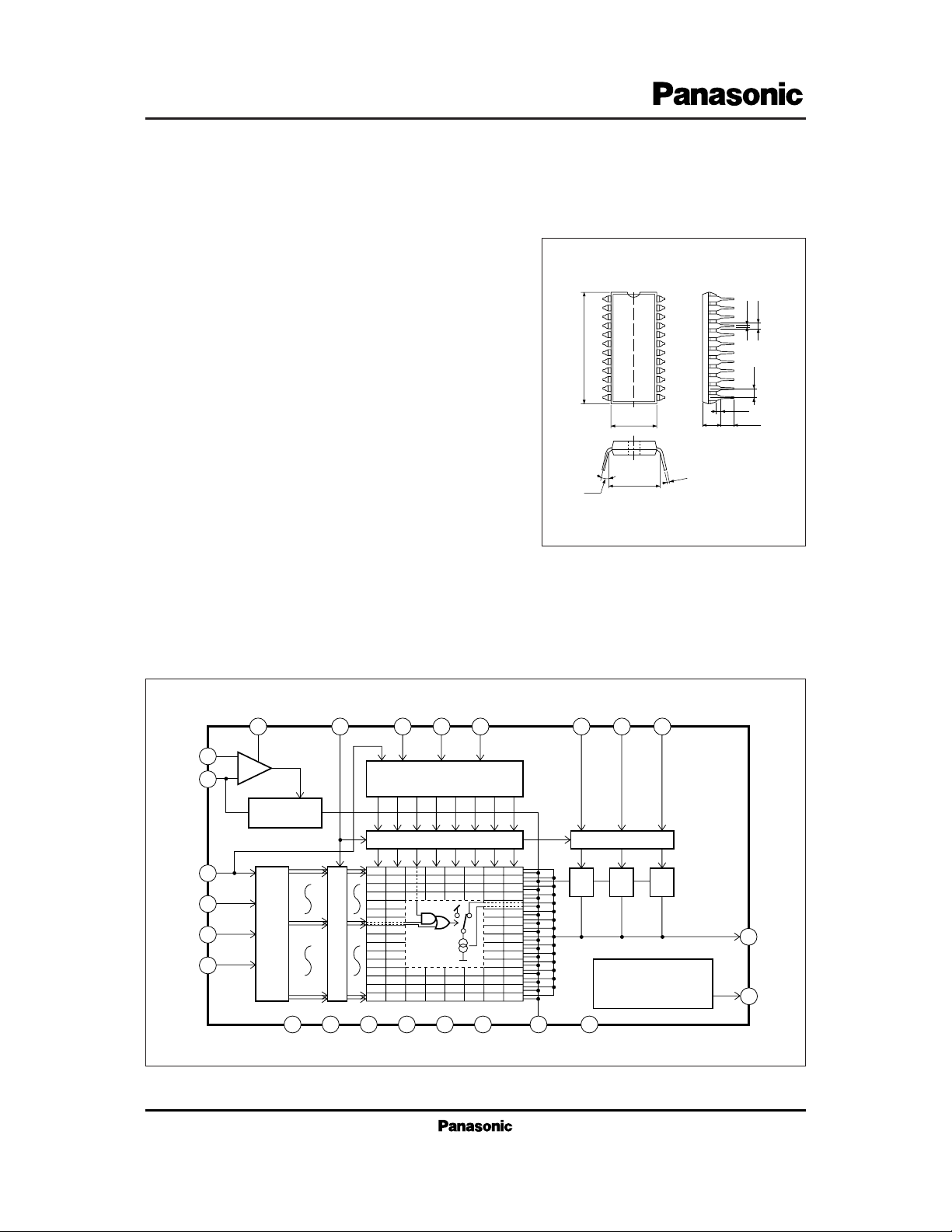
24-pin Shrunk DIL Plastic Package (SDIP024-P-0300)
7.62±0.25
21.7±0.3
0.3±
+ 0.2
– 0.05
3 ∼15˚
6.2±0.3
0.5±0.1
0.9±0.25
1.778
4.7±0.25
3.05±0.25
1.1±0.25
1
2
3
4
5
6
7
8
9
10
11
12
24
23
22
21
20
19
18
17
16
15
14
13
■ Block Diagram
REFI
IREF
D6
D7
D8
D9
(MSB)
COMP CLK D5 D4 D3 D2 D1
9 14 19 20 21 22 23 24
+
7
10
18
17
16
15
–
Current
Source
X– Decoder
AGND DV
Latch
DGND AVCCAV
CC
X – Decoder
Latch
CC
AGND
VIB NC
1/2 1/4 1/8
8 13 13 2 11 12 4
(LSB)
D0
Latch
Reference
Voltage Regulator
OUT
5
6
REFO
2
A/D and D/A Converters
AN8140K
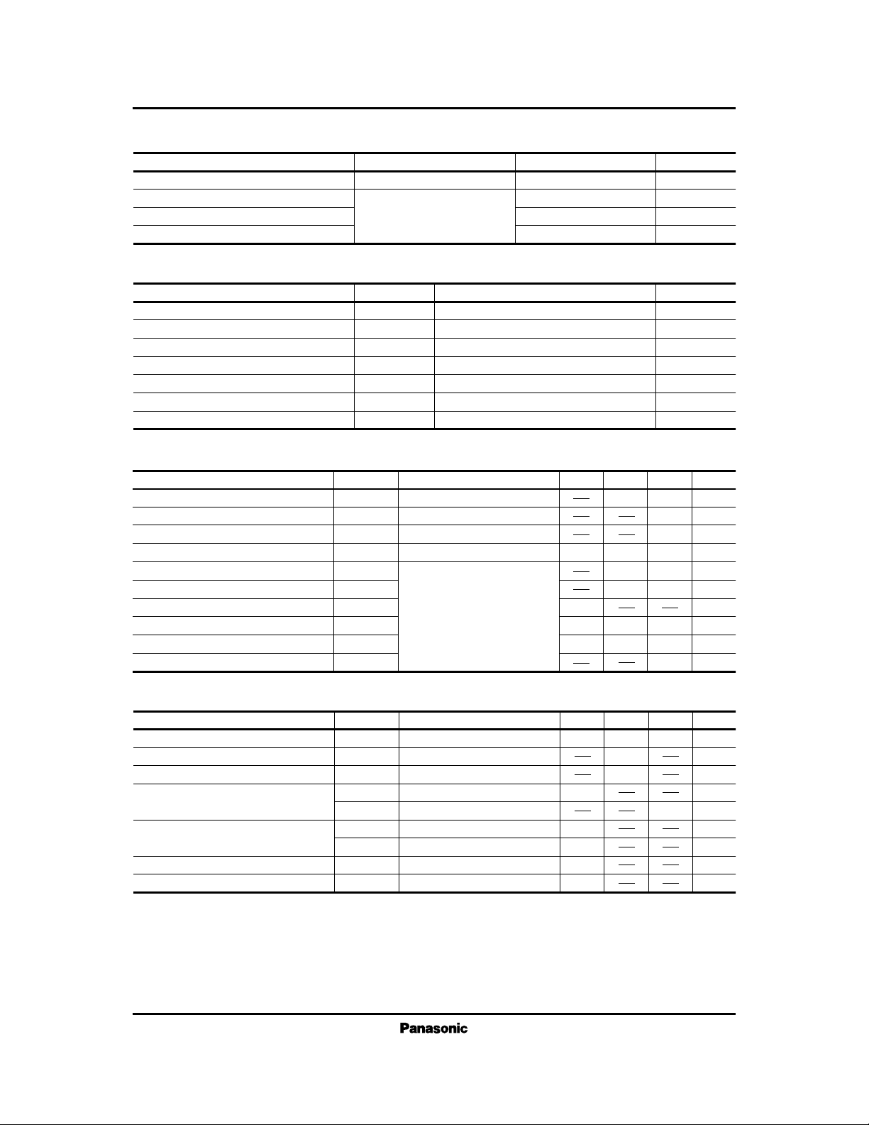
Parameter Condition Rating Unit
Resolution 10 bit
Linearity error R
REF
= 470Ω ±1.0 LSB
Differential linearity error R
O
= 75Ω ±1.0 LSB
Maximum conversion rate V
REFO –VREFI
= 1.4V 50 MSPS
■ Main Characteristics (VCC=5.0V, Ta=25˚C)
V
CC
V
IN
I
O
V
REFI
P
D
T
opr
T
stg
Supply voltage
Digital input voltage
Analogue output current
Reference input voltage
Power dissipation
Operating ambient temperature
Storage temperature
V
V
mA
V
mW
˚C
˚C
Paremeter Symbol Rating Unit
■ Absolute Maximum Rating (Ta=25˚C)
– 0.3 to +7.0
– 0.3 to DV
CC
30
– 0.3 to AV
CC
700
–20 to + 70
–55 to +150
VIN= 0V, 5V
VIN= 0V, 5V
I
REFO
= 3.0mA
Parameter Symbol Rating min typ max Unit
■ Electrical Characteristics (VCC=5.0V, Ta=25˚C)
I
CC
I
LK1
I
LK2
V
REFO
E
L
E
D
F
C
V
FS
V
ZS
t
ST
2.16
50
4.9
3.8
30
2.7
±0.5
±0.5
5.0
4.0
50
±30
±30
3.24
±1
±1
5.1
4.2
20
mA
µA
µA
V
LSB
LSB
MSPS
V
V
ns
Supply current
Digital input leak current
REFI input leak current
Reference output voltage
Linearty error
Differential linearty error
Maximum conversion rate
Full-scale output voltage
Zero-scale output voltage
Settling time
R
REF
= 470Ω
RO= 75Ω
V
REF0 –VREFI
= 1.4V
Parameter Symbol Conditions min typ max Unit
Supply voltage V
CC
4.75 5.0 5.25 V
Regerence voltage v
REFO
= 2.7V V
REFI
RO = 75Ω, R
REF
= 470Ω 1.3 V
Output load resistance R
O
75 Ω
Digital input voltage
V
IH
2.4 V
V
IL
0.8 V
Clock input pulse width
t
WH
*1 8 *2 ns
t
WL
*1 8 *2 ns
Setting-up time t
S
*1 5 ns
Holding time t
H
*1 1 ns
■ Recommended Operating Conditions (Ta=25˚C)
*1 : Refer to the timing chart.
*2 : tWH+tWL≥20ns
 Loading...