

Panasonic AN80xx, AN80xxM Technical data
查询AN80xx Series供应商
Voltage Regulators
AN80xx/AN80xxM Series
3-pin, positive output, low dropout voltage regulator (50 mA type)
■ Overview
The AN80xx series and the AN80xxM series are 3pin, low dropout, fixed positive output type monolithic
voltage regulators. Since their power consumption can
be minimized, they are suitable for battery-used power
supply and reference voltage. 13 types of output voltage
are available; 2V, 2.5V, 3V, 3.5V (SSIP003-P-0000 only),
4V, 4.5V, 5V, 6V, 7V, 8V, 8.5V, 9V, and 10V.
■ Features
• Input/output voltage difference: 0.3V max.
• Output current of up to 50mA
• Low bias current: 0.6mA typ.
• Output voltage: 2V, 2.5V, 3V, 3.5V (SSIP003-P-0000
only), 4V, 4.5V, 5V, 6V, 7V, 8V, 8.5V, 9V, and 10V
• Built-in overcurrent protection circuit
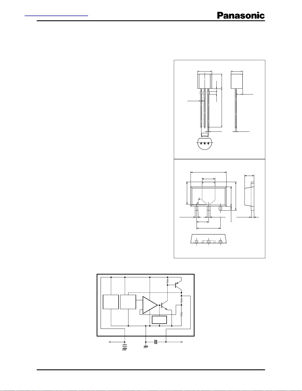
AN80xx series Unit: mm
0.6±0.15
5.0±0.2
(1.0)(1.0)
+0.1
0.43
–0.05
2.54
213
SSIP003-P-0000
5.1±0.213.5±0.5
4.0±0.2
0.43
2.3±0.2
+0.1
–0.05
1: Input
2: Output
3: GND
AN80xxM series Unit: mm
4.6 max.
1.8 max.
2.6
45°
2.6 max.
4.25 max.
1.6 max.
■ Block Diagram (AN80xxM series)
Starter
V
I
0.48 max.
0.58 max.
1.5
3.0
123
0.8 min.
HSIP003-P-0000B
Voltage
Reference
3
(1)
C
+
Error
Amp.
−
Current
Limiter
2
(3)
IN
1
−
+
(2)
C
OUT
R
2
R
1
R1 = 5kΩ
= 0.33µF
C
IN
= 10µF
C
V
O
OUT
Note) The number in ( ) shows the pin number for the AN80xx series.
0.44 max.
1: Output
2: GND
3: Input
Publication date: August 2001 SFF00007AEB
1
AN80xx/AN80xxM Series
■ Absolute Maximum Ratings at Ta = 25°C
Parameter Symbol Rating
Supply voltage
Supply current
Power dissipation
Operating ambient temperature
Storage temperature
*
AN80xxM series is mounted on standard board (glass epoxy: 20mm × 20mm × t1.7mm with Cu foil of 1cm
■ Electrical Characteristics at T
AN80xx series
AN80xxM series
= 25°C
a
V
I
I
CC
P
D
T
opr
T
stg
20
100
*
650
−30 to +80
−55 to +150
−55 to +125
2
or more).
Unit
V
mA
mW
°C
°C
• AN8002, AN8002M (2V type)
Parameter Symbol Conditions Min Typ Max
Output voltage
Line regulation
Load regulation
Minimum input/output voltage difference
Bias current
Ripple rejection ratio
Output noise voltage
Output voltage temperature coefficient
V
REG
REG
V
DIF(min)
I
Bias
RR
V
∆VO/T
T
= 25°C
O
no
j
IN
I
= 1 to 40mA, Tj = 25°C
O
L
I
= 1 to 50mA, Tj = 25°C
O
V
I
V
I
I
= 0mA, Tj = 25°C
O
V
I
f = 10Hz to 100kHz
Tj = −30 to +125°C
a
= 1.9V, IO = 20mA, Tj = 25°C
= 1.9V, IO = 50mA, Tj = 25°C
= 3 to 5V, f = 120Hz
1.92
62
2.08 V2
2
7
10
0.12
74
60
Note 1) The specified condition Tj = 25°C means that the test should be carried out within so short a test time (within 10ms) that the
characteristic value drift due to the chip junction temperature rise can be ignored.
Note 2) Unless otherwise specified, V
= 3V, IO = 20mA and CO = 10µF.
I
Unit
40
mVVI = 2.5 to 8V, Tj = 25°C
20 mV
mV
25
0.2
0.3
1
mA0.6
mV/°C0.1
V0.06
V
dB
µV
•
AN8025, AN8025M (2.5V type)
2.62.5
50
20
25
0.2
0.3
Unit
V
mV
mV
mV
V
V
1
mAI
dBRR
µVV
mV/°C∆VO/T
Parameter Symbol Conditions Min Typ Max
Output voltage
Line regulation
Load regulation
Minimum input/output voltage difference
Bias current
Ripple rejection ratio
Output noise voltage
Output voltage temperature coefficient
REG
REG
V
DIF(min)
T
V
O
Bias
no
= 25°C
j
V
= 3 to 8.5V, Tj = 25°C
I
IN
I
= 1 to 40mA, Tj = 25°C
O
L
I
= 1 to 50mA, Tj = 25°C
O
= 2.4V, IO = 20mA, Tj = 25°C
V
I
= 2.4V, IO = 50mA, Tj = 25°C
V
I
I
= 0mA, Tj = 25°C
O
= 3.5 to 5.5V, f = 120Hz
V
I
f = 10Hz to 100kHz
T
= −30 to +125°C
j
a
2.4
60
2.5
8
12.5
0.07
0.12
0.6
72
65
0.13
Note 1) The specified condition Tj = 25°C means that the test should be carried out within so short a test time (within 10ms) that the
characteristic value drift due to the chip junction temperature rise can be ignored.
Note 2) Unless otherwise specified, V
= 3.5V, IO = 20mA and CO = 10µF.
I
2
SFF00007AEB
AN80xx/AN80xxM Series
yp
■ Electrical Characteristics at Ta = 25°C (continued)
•
AN8003, AN8003M (3V type)
50
25
30
0.2
0.3
50
30
40
0.2
0.3
Unit
V
mV
mV
mV
V
V
1
mAI
dBRR
µVV
mV/°C∆VO/T
Unit
V
mV
mV
mV
V
V
1
1
mAI
dBRR
µVV
mV/°C∆VO/T
Parameter Symbol Conditions Min Typ Max
Output voltage
Line regulation
Load regulation
Minimum input/output voltage difference
Bias current
Ripple rejection ratio
Output noise voltage
Output voltage temperature coefficient
REG
REG
V
DIF(min)
V
Bias
T
= 25°C
O
no
j
V
I
IN
I
= 1 to 40mA, Tj = 25°C
O
L
I
= 1 to 50mA, Tj = 25°C
O
V
I
V
I
= 0mA, Tj = 25°C
I
O
V
I
f = 10Hz to 100kHz
= −30 to +125°C
T
j
a
= 3.5 to 9V, Tj = 25°C
= 2.9V, IO = 20mA, Tj = 25°C
= 2.9V, IO = 50mA, Tj = 25°C
= 4 to 6V, f = 120Hz
2.88
58
3.123
3
9
15
0.07
0.12
0.6
70
70
0.15
Note 1) The specified condition Tj = 25°C means that the test should be carried out within so short a test time (within 10ms) that the
characteristic value drift due to the chip junction temperature rise can be ignored.
Note 2) Unless otherwise specified, V
•
AN8035(3.5V type)
= 4V, IO = 20mA and CO = 10µF.
I
Parameter Symbol Conditions Min Typ Max
Output voltage
Line regulation
Load regulation
Minimum input/output voltage difference
Bias current
Ripple rejection ratio
Output noise voltage
Output voltage temperature coefficient
REG
REG
V
DIF(min)
V
Bias
T
= 25°C
O
no
j
V
I
IN
I
= 1 to 40mA, Tj = 25°C
O
L
I
= 1 to 50mA, Tj = 25°C
O
V
I
V
I
= 0mA, Tj = 25°C
I
O
V
I
f = 10Hz to 100kHz
T
= −30 to +125°C
j
a
= 4 to 9.5V, Tj = 25°C
= 3.4V, IO = 20mA, Tj = 25°C
= 3.4V, IO = 50mA, Tj = 25°C
= 4.5 to 6.5V, f = 120Hz
3.36
57
3.643.5
3.5
10
20
0.07
0.12
0.6
69
75
0.2
Note 1) The specified condition Tj = 25°C means that the test should be carried out within so short a test time (within 10ms) that the
characteristic value drift due to the chip junction temperature rise can be ignored.
Note 2) Unless otherwise specified, V
= 4.5V, IO = 20mA and CO = 10µF.
I
•
AN8004, AN8004M (4V type)
50
30
40
0.2
0.3
Unit
V
mV
mV
mV
V
V
1
mAI
dBRR
µVV
mV/°C∆VO/T
Parameter Symbol Conditions Min Typ Max
Output voltage
Line regulation
Load regulation
Minimum input/output voltage difference
Bias current
Ripple rejection ratio
Output noise voltage
Output voltage temperature coefficient
REG
REG
V
DIF(min)
T
V
O
Bias
no
= 25°C
j
V
= 4.5 to 10V, Tj = 25°C
I
IN
I
= 1 to 40mA, Tj = 25°C
O
L
I
= 1 to 50mA, Tj = 25°C
O
= 3.8V, IO = 20mA, Tj = 25°C
V
I
= 3.8V, IO = 50mA, Tj = 25°C
V
I
= 0mA, Tj = 25°C
I
O
= 5 to 7V, f = 120Hz
V
I
f = 10Hz to 100kHz
= −30 to +125°C
T
j
a
3.84
56
4.164
3.5
10
20
0.07
0.12
0.6
67
80
0.2
Note 1) The specified condition Tj = 25°C means that the test should be carried out within so short a test time (within 10ms) that the
characteristic value drift due to the chip junction temperature rise can be ignored.
Note 2) Unless otherwise specified, V
= 5V, IO = 20mA and CO = 10µF.
I
SFF00007AEB
3
 Loading...