

Panasonic 2SD1119 Datasheet
Transistor
2SD1119
Silicon NPN epitaxial planer type
For low-frequency power amplification
Features
■
●
Low collector to emitter saturation voltage V
●
Satisfactory operation performances at high efficiency with the
low-voltage power supply.
●
Mini type package, allowing downsizing of the equipment and
automatic insertion through the tape packing and the magazine
packing.
Absolute Maximum Ratings (Ta=25˚C)
■
Parameter
Collector to base voltage
Collector to emitter voltage
Emitter to base voltage
Peak collector current
Collector current
Collector power dissipation
Junction temperature
Storage temperature
*
Printed circuit board: Copper foil area of 1cm2 or more, and the board
thickness of 1.7mm for the collector portion
Symbol
V
CBO
V
CEO
V
EBO
I
CP
I
C
*
P
C
T
j
T
stg
Ratings
40
25
150
–55 ~ +150
7
5
3
1
CE(sat)
.
Unit
V
V
V
A
A
W
˚C
˚C
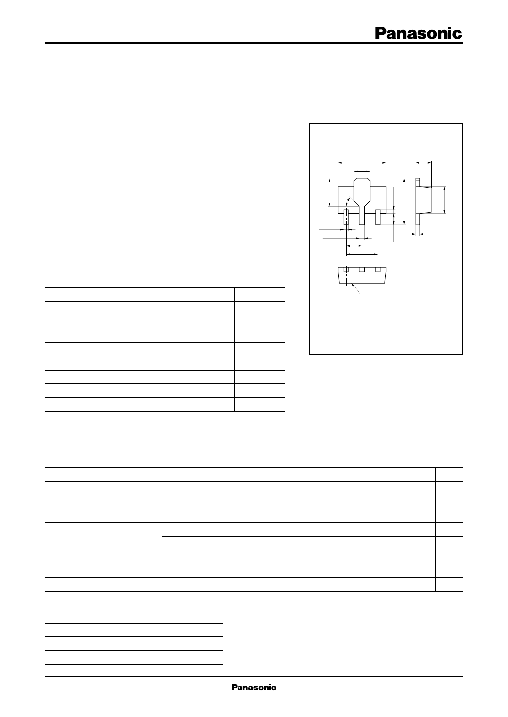
4.5±0.1
1.6±0.2
2.6±0.1
45°
0.4±0.08
0.5±0.08
1.5±0.1
3.0±0.15
321
marking
1:Base
2:Collector EIAJ:SC–62
3:Emitter Mini Power Type Package
1.5±0.1
–0.20
+0.25
0.4max.1.0
4.0
–0.2
+0.1
Marking symbol : T
Unit: mm
2.5±0.1
0.4±0.04
Electrical Characteristics (Ta=25˚C)
■
Parameter
Collector cutoff current
Collector to emitter voltage
Emitter to base voltage
Forward current transfer ratio
Collector to emitter saturation voltage
Transition frequency
Collector output capacitance
*1
h
Rank classification
FE1
Symbol
I
CBO
V
CEO
V
EBO
h
FE1
h
FE2
V
CE(sat)
f
T
C
ob
Rank Q R
h
FE1
230 ~ 380 340 ~ 600
Marking Symbol TQ TR
Conditions
VCB = 10V, IE = 0
IC = 1mA, IB = 0
IE = 10µA, IC = 0
*1
VCE = 2V, IC = 0.5A
VCE = 2V, IC = 2A
IC = 3A, IB = 0.1A
*2
*2
*2
VCB = 6V, IE = –50mA, f = 200MHz
VCB = 20V, IE = 0, f = 1MHz
min
25
230
150
typ
max
0.1
Unit
µA
V
7
V
600
150
50
*2
Pulse measurement
1
V
MHz
pF
1
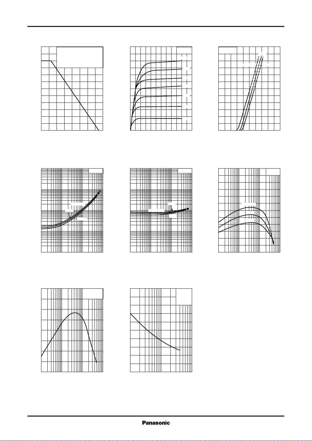
Transistor
2SD1119
PC — Ta IC — V
1.2
)
W
(
1.0
C
0.8
0.6
0.4
0.2
Collector power dissipation P
0
)
10
V
(
3
CE(sat)
1
0.3
0.1
0.03
0.01
0.003
0.001
Collector to emitter saturation voltage V
0.01 0.1 1 100.03 0.3 3
Printed circut board: Copper
foil area of 1cm
the board thickness of 1.7mm
for the collector portion.
0 16040 12080 14020 10060
2
or more, and
Ambient temperature Ta (˚C
V
— I
CE(sat)
C
IC/IB=30
Ta=75˚C
25˚C
–25˚C
Collector current IC (A
)
)
CE
2.4
2.0
)
A
(
1.6
C
1.2
0.8
Collector current I
0.4
0
0 2.42.01.60.4 1.20.8
Ta=25˚C
IB=7mA
6mA
5mA
4mA
3mA
2mA
1mA
Collector to emitter voltage VCE (V
V
— I
BE(sat)
100
)
V
(
30
BE(sat)
10
3
1
0.3
0.1
0.03
Base to emitter saturation voltage V
0.01
0.01 0.1 1 100.03 0.3 3
Ta=–25˚C
Collector current IC (A
C
IC/IB=30
25˚C
75˚C
)
IC — V
6
VCE=2V
5
)
A
(
4
C
3
2
Collector current I
1
0
02.01.60.4 1.20.8
)
Base to emitter voltage VBE (V
hFE — I
600
FE
500
400
300
200
100
Forward current transfer ratio h
0
0.01 0.1 1 100.03 0.3 3
Collector current IC (A
Ta=75˚C
Ta=75˚C
25˚C
–25˚C
BE
25˚C
–25˚C
)
C
=2V
V
CE
)
400
350
)
MHz
300
(
T
250
200
150
100
Transition frequency f
50
0
– 0.01
– 0.1 –1 –10
– 0.03
Emitter current IE (A
2
fT — I
E
– 0.3 –3
VCB=6V
Ta=25˚C
)
)
pF
(
Cob — V
100
80
ob
60
40
20
CB
Collector output capacitance C
0
1 3 10 30 100
Collector to base voltage VCB (V
IE=0
f=1MHz
Ta=25˚C
)
 Loading...