

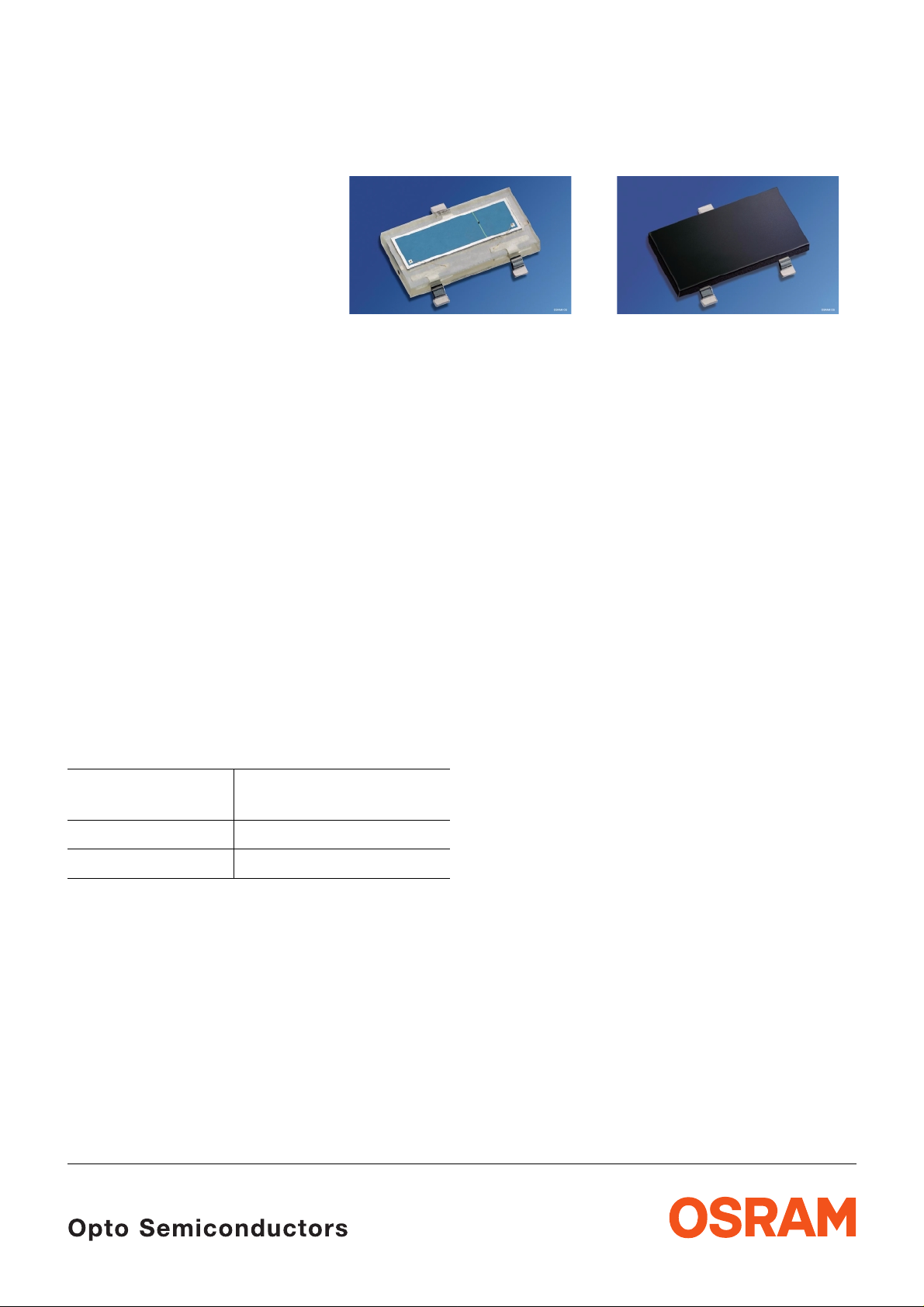
2fach-Silizium-PIN Fotodiode in SMT
2-Chip Silicon PIN Photodiode in SMT
KOM 2125
KOM 2125 FA
KOM 2125 KOM 2125 FA
Wesentliche Merkmale
• Speziell geeignet für Anwendungen im Bereich
von 400 nm bis 1100 nm und bei 880 nm
(KOM 2125 FA)
• Kurze Schaltzeit (typ. 25 ns)
• geeignet für Vapor-Phase Löten und
IR-Reflow-Löten
• SMT-fähig
Anwendungen
• Nachlaufsteuerungen
• Kantenführung
• Industrieelektronik
• „Messen/Steuern/Regeln“
Typ
Type
KOM 2125 Q62702-K0047
KOM 2125 FA Q62702-P5313
Bestellnummer
Ordering Code
Features
• Especially suitable for applications from
400 nm to 1100 nm and of 880 nm
(KOM 2125 FA)
• Short switching time (typ. 25 ns)
• Suitable for vapor-phase and IR-reflow
soldering
• Suitable for SMT
Applications
• Follow-up controls
• Edge drives
• Industrial electronics
• For control and drive circuits
2001-02-21 1
Grenzwerte
Maximum Ratings
KOM 2125, KOM 2125 FA
Bezeichnung
Parameter
Betriebs- und Lagertemperatur
Operating and storage temperature range
Sperrspannung
Reverse voltage
Verlustleistung,
T
= 25 °C
A
Total power dissipation
T
Kennwerte (
Characteristics (
= 25 °C)
A
T
= 25 °C)
A
Bezeichnung
Parameter
Fotostrom
Photocurrent
V
= 5 V, Normlicht/standard light A
R
T = 2856 K, E
V
= 5 V, λ = 870 nm,Ee = 1mW/cm2
R
= 1000 Ix
v
Diode A
Diode B
Diode A
Diode B
Symbol
Symbol
T
; T
op
V
R
P
tot
Symbol
Symbol
I
P
I
P
Wert
Value
stg
– 40 … +80 °C
60 V
150 mW
Wert
Value
KOM 2125 KOM 2125 FA
40 (> 30)
100 (> 75)
–
–
–
–
26 (> 20)
70 (> 50)
Einheit
Unit
Einheit
Unit
µA
µA
Wellenlänge der max. Fotoempfindlichkeit
Wavelength of max. sensitivity
Spektraler Bereich der Fotoempfindlichkeit
S = 10% von S
max
Spectral range of sensitivity
S = 10% of S
max
Bestrahlungsempfindliche Fläche Diode A
Radiant sensitive area Diode B
Abmessung der
bestrahlungsempfindlichen Fläche
Dimensions of radiant sensitive area
Diode A
Diode B
Abstand Chipoberfläche zu Vergußoberfläche
Distance chip front to case seal
Halbwinkel
Half angle
Dunkelstrom,
V
= 10 V Diode A
R
Dark current Diode B
λ
S max
850 900 nm
λ 400 … 1100 750 ... 1100 nm
A
L × B
L
× W
H
4
10
2 × 2
2 × 5
0.3 0.3 mm
4
10
2 × 2
2 × 5
mm
mm × mm
mm × mm
ϕ±60 ± 60 Grad
deg.
I
R
5 (≤ 30)
10 (≤ 30)
5 (≤ 30)
10 (≤ 30)
nA
2
2001-02-21 2

Kennwerte (TA = 25 °C)
Characteristics (
T
= 25 °C) (cont’d)
A
Bezeichnung
Parameter
Leerlaufspannung
Open-circuit voltage
E
= 1000 Ix, Normlicht/standard light A
v
E
= 1 mW/cm2, λ = 850 nm
e
Kurzschlussstrom
Short-circuit current
Normlicht/standard light A
T = 2856 K, E
λ
= 870 nm, E
= 1000 Ix
v
= 1 mW/cm
e
2
Diode A
Diode B
Diode A
Diode B
Symbol
Symbol
V
O
V
O
I
SC
I
SC
KOM 2125, KOM 2125 FA
Wert
Value
KOM 2125 KOM 2125 FA
350 (> 300)––
350 (> 300)
38
95
–
–
–
–
24
66
Einheit
Unit
mV
mV
µA
µA
Anstiegszeit/Abfallzeit Diode A
Rise and fall time Diode B
R
= 50 Ω; VR = 5 V;
L
= 850 nm; I
λ
Durchlassspannung,
= 800 µA
P
I
= 100 mA; E = 0
F
Forward voltage
Kapazität Diode A
Capacitance Diode B
V
= 0 V; f = 1 MHz; E = 0
R
Temperaturkoeffizient von
Temperature coefficient of V
Temperaturkoeffizient von
Temperature coefficient of I
V
O
O
I
P
P
Normlicht/standard light A
λ
= 850 nm
Rauschäquivalente
Strahlungsleistung Diode A
Noise equivalent power Diode B
V
= 10 V
R
Nachweisgrenze, VR = 10 V Diode A
Detection limit Diode B
t
r, tf
18
25
V
C
F
0
1.0 1.0 V
40
100
TC
TC
V
I
– 2.6 – 2.6 mV/K
0.18
–
NEP 6.4 × 10
9.1 × 10
D* 3.1 × 10
3.5 × 10
– 14
– 14
12
12
18
25
40
100
–
0.2
6.4 × 10
9.1 × 10
3.1 × 10
3.5 × 10
– 14
– 14
12
12
ns
pF
%/K
W
----------- Hz
cm Hz×
-------------------------W
2001-02-21 3

KOM 2125, KOM 2125 FA
Relative Spectral Sensi tivity
KOM 2125,
Dark Current,
S
= f (λ)
rel
I
= f (VR), E = 0
R
normalized to 10 V/25 °C
Relative Spectral Sensitivity
KOM 2125 FA,
100
S
rel
%
80
70
60
50
40
30
20
10
0
400
S
= f (λ)
rel
600 800 1000 nm 1200
OHF01430
λ
Capacitance
C = f (V
), f = 1 MHz, E = 0
R
Photocurrent IP = f (Ev), VR = 5 V
Open-Circuit Voltage
Dark Current
I
R
E = 0, normalized to T
V
= f (Ev)
O
= f (TA), VR = 10 V,
= 25 °C
A
Directional Character i sti cs
S
= f (ϕ)
rel
100
40 30 20 10
50
60
70
80
90
0
ϕ
1.0
0.8
0.6
0.4
0.2
0
20 40 60 80 100 1200.40.60.81.0
0
2001-02-21 4
OHF01402
Total Powe r Dissipatio n
P
= f (TA)
tot

Maßzeichnung
Package Outlines
Photosensitive area
A = 2 (0.079) x 2 (0.079)
B = 5 (0.197) x 2 (0.079)
5.2 (0.205)
5.0 (0.197)
23
A
B
1
8.5 (0.335)
Cathode
8.2 (0.323)
0.9 (0.035)
0.7 (0.028)
±0.2 (0.008)
1.4 (0.055)
4.5 (0.177)
6.7 (0.264)
6.2 (0.244)
4.3 (0.169)
KOM 2125, KOM 2125 FA
Chip position
0...0.1 (0...0.004)
0.3 (0.012)
Active area
1.2 (0.047)
1.1 (0.043)
GEOY6860
Maße werden wie folgt angegeb en: m m (inch) / Dimensions are specified as follo w s: m m (inc h).
Published by OSRAM Opto Semiconductors GmbH & Co. OHG
Wernerwerkstrasse 2, D-93049 Regensburg
© All Rights Reserved.
Attention please!
The information describes the type of component and shall not be considered as assured char ac te ris tics .
Terms of delivery and rights to change design reserved. Due to technical requirements components may contain
dangerous substances. For information on the types in question please contact our Sales Organization.
Packing
Please use the recycling operators k nown to you . We can als o help you – get in touch wit h your near est sales offic e.
By agreement we will take p acking material back, if it is sorted. You m ust bear the costs of transport. For packing
material that is returned to us unsorted or which we are not obliged to accept, we shall have to invoice you for any costs
incurred.
Components used in life-support devices or systems must be expressly authorized for such purpose! Critical
components
1
A critical component is a co mponent usedin a l ife-support devi ce or system whose failure can re asonably be expec ted
1
, may only be used in life-support devices or systems 2 with the express written approval of OSRAM OS.
to cause the failure of that life-support device or system, or to affect its safety or effectiveness of that device or system.
2
Life support devices or systems are intend ed (a) to be impl anted i n t he human b ody , or (b ) to supp ort a nd/or ma inta in
and sustain human life. If th ey fail , it is rea so nable to assume that the health of the us er m ay be endangered.
2001-02-21 5
 Loading...