

Page 1
TV29LB929
SERVICE MANUAL
LCD/LED-TV
ORIGINAL
CHASSIS CODE A
Design and specifications are subject to change without notice.
Page 2
SERVICING NOTICES ON CHECKING
required.
External exposure metal:
1. KEEP THE NOTICES 6. PERFORM A SAFETY CHECK AFTER
SERVICING
As for the places which need special attentions,
they are indicated with the labels or seals on the Confirm that the screws, parts and wiring which
cabinet, chassis and parts. Make sure to keep the were removed in order to service are put in the
indications and notices in the operation manual. original positions, or whether there are the
portions which are deteriorated around the
2. AVOID AN ELECTRIC SHOCK serviced places serviced or not. Check the
insulation between the antenna terminal or
There is a high voltage part inside. Avoid an external metal and the AC cord plug blades.
electric shock while the electric current is And be sure the safety of that.
flowing.
(INSULATION CHECK PROCEDURE)
3. USE THE DESIGNATED PARTS
1. Unplug the plug from the AC outlet.
The parts in this equipment have the specific 2. Remove the antenna terminal on TV and turn
characters of incombustibility and withstand on the TV.
voltage for safety. Therefore, the part which is 3. Insulation resistance between the cord plug
replaced should be used the part which has terminals and the eternal exposure metal
the same character. [Note 2] should be more than 1M ohm by
Especially as to the important parts for safety using the 500V insulation resistance meter
which is indicated in the circuit diagram or the [Note 1].
table of parts as a ! mark, the designated 4. If the insulation resistance is less than 1M
parts must be used. ohm, the inspection repair should be
4. BE CAREFUL WITH THE
LCD PANEL [Note 1]
If you have not the 500V insulation
Avoid a shock to the panel while servicing. resistance meter, use a Tester.
Take enough care to deal with it.
[Note 2]
5. PUT PARTS AND WIRES IN THE
ORIGINAL POSITION AFTER Headphone jack
ASSEMBLING OR WIRING
There are parts which use the insulation
material such as a tube or tape for safety, or
which are assembled in the condition that
these do not contact with the printed board.
The inside wiring is designed not to get closer
to the pyrogenic parts and high voltage parts.
Therefore, put these parts in the original
positions.
Antenna terminal
HOW TO ORDER PARTS
Please include the following informations when you order parts. (Particularly the CHASSIS CODE.)
1. MODEL NUMBER and CHASSIS CODE
YOU can find it in the back of your unit.
2. PART NO. and DESCRIPTION
You can find it in your SERVICE MANUAL.
IMPORTANT
When you exchange IC and Transistor with a heat sink, apply silicon grease (YG6260M) on the contact
section of the heat sink. Before applying new silicon grease, remove all the old silicon grease.
(Old grease may cause damage to the IC and Transistor).
A1-1
Page 3
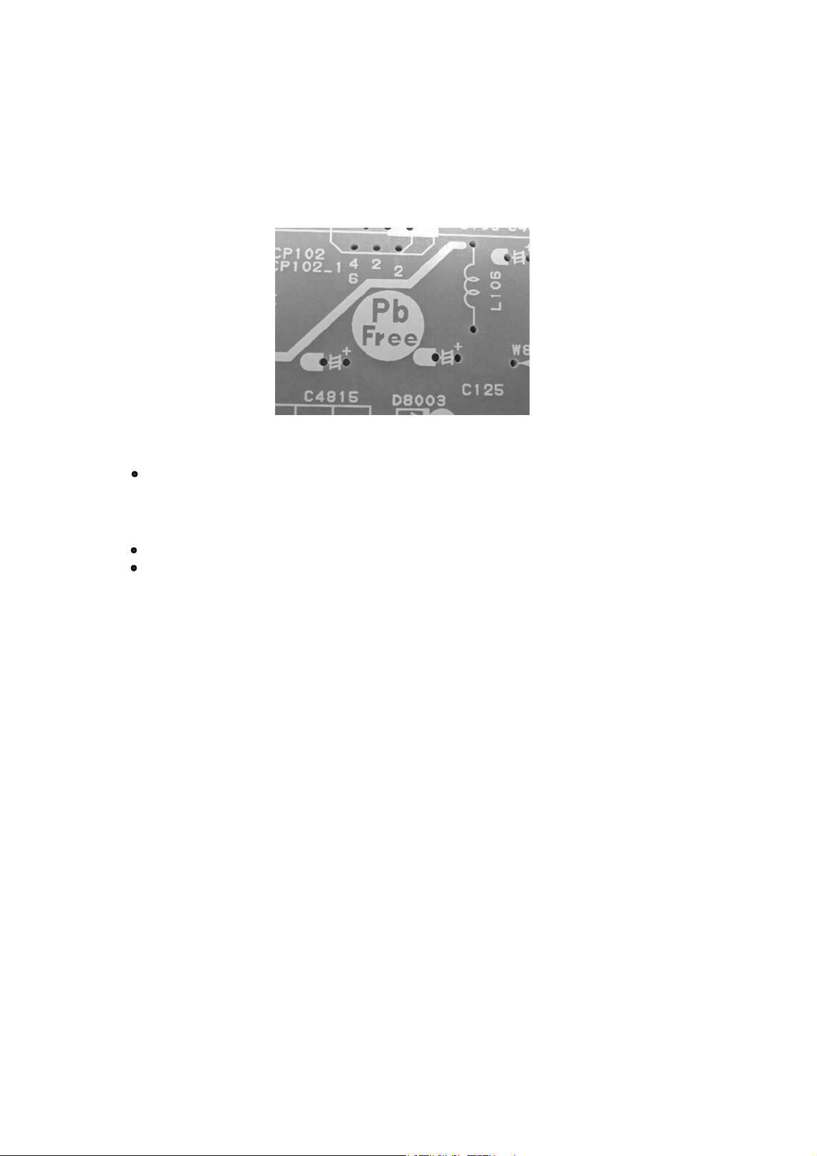
ABOUT LEAD FREE SOLDER (PbF)
Distinction of PbF PCB:
PCB's (manufactured) using lead free solder will have a PbF printing on the PCB.
(Please refer to figures.)
Caution:
Pb free solder has a higher melting point than standard solder;
Typically the melting point is 86
Please use a soldering iron with temperature control and adjust it to 650
In case of using high temperature soldering iron, please be careful not to heat too long.
Pb free solder will tend to splash when heated too high (about 1100oF/ 600oC).
All products with the printed circuit board with PbF printing must be serviced with lead free solder.
When soldering or unsoldering, completely remove all of the solder from the pins or solder area,
and be sure to heat the soldering points with the lead free solder until it melts sufficiently.
o
F~104oF(30oC~40oC) higher.
o
F ± 20oF (350oC ±10oC).
Recommendations
Recommended lead free solder composition is Sn-3.0Ag-0.5Cu.
A1-2
Page 4
HOTEL MODE FUNCTION
7.Select the Clear Lock menu, then press ENTER button
To set the Hotel mode, please follow the steps below.
1. Press the MENU ---> 1147 button on the remote control. Hotel mode On
2. Press the DOWN button on the remote control, Source Lock
3. Select the "Setup" menu , then press ENTER button. Tuning Lock Off
Select the "Hotel Mode" menu, Select "On".
4.
The Hotel mode setting menu will appear.
5.
Using the UP/DOWN button on the remote control,
6.
select the desired mode. Then press the ENTER button.
7. Using the LEFT/RIGHT button on the remote control, Default Volume
set the mode to desired setting. Clone to USB
8. The Hotel mode has now been set up. Restore from USB
Default Source Off
Channel Type All
Default Program None
Max Volume
Clear Lock
To reset the Hotel mode, please follow the steps below.
1. Press the MENU ---> 1147 button on the remote control.
2. Press the DOWN button on the remote control,
3. Select the "Setup" menu , then press ENTER button.
Select the "Hotel Mode" menu, Select "On".
4.
The Hotel mode setting menu will appear.
5.
6. Press the DOWN button on the remote control,
"
8. The setting items has now been returned to initial value.
Setting item Setting value
"
Initial value
.
FUNCTION
<>
>>
<>
<>
<>
<>
100
50
>>
>>
>>
ANTENNA/CABLE/
Source Lock
Tunning Lock OFF/ON
Default Source
Channel Type ALL
Default Program
Default Volume
Clone to USB
SATELLITE/AV
COMPONENT/
HDMI/USB
OFF/ANTENNA/CABLE/
SATELLITE/AV Setting Input Source, combine with "Source Lock"
COMPONENT/ If select "Source Lock" for this function disappear.
HDMI/USB
ALL/DIGITAL/RADIO/ Setting of the CH if select "Default Source" to ALL/
ANALOGUE ANTENNA/CABLE/SATELLITE input.
NONE NONE/1/2/3/…/197
0~100
Setting Input skip, combine with "Default Source".
Setting of the tunning Lock. When turn on “Tuning lock”,
User cannot choose the following item in MENU.
OFF
OFF
100Max volume 0~100
50 Setting volume at Power on.
(skip an item and not available.)
Tuner Mode, Channels, Satellite Setup, First time installation,
Reset Default, Clean All
Setting of the CH if select "Default Source" to ANTENNA/
CABLE/SATELLITE input.
Setting of the maximum volume value.
Copy to USB about User Menu setting, Hotel Mode setting
and stored channels.
Restore from USB
Clear Lock
Read and Restore data from USB that is saved by Cone
to USB.
Setting of the Hotel Mode return factory setting.
A1-3
Page 5

…
…
…
…
…
…
…
…
…
…
TABLE OF CONTENTS
SERVICING NOTICES ON CHECKING…………………………………………………………………
HOW TO ORDER PARTS…………………………………………………………………………………
IMPORTANT………………………………………………………………………………………………
ABOUT LEAD FREE SOLDER (PbF)…………………………………………………………………
HOTEL MODE FUNCTION………………………………………………………………………………
TABLE OF CONTENTS…………………………………………………………………………………
GENERAL SPECIFICATIONS……………………………………………………………………………
DISASSEMBLY INSTRUCTIONS
1. REMOVAL OF MECHANICAL PARTS AND P. C. BOARDS……………………………………B1-1, B1-2
2. REMOVAL AND INSTALLATION OF FLAT PACKAGE IC………………………………………B2-1, B2-2
SERVICE MODE LIST……………………………………………………………………………………
ELECTRICAL ADJUSTMENTS…………………………………………………………………………
BLOCK DIAGRAM ………………………………………………………………………………………
PRINTED CIRCUIT BOARDS
POWER ………………………………………………………………………………………………… F-1, F-2
OPERATION/REMOCON ………………………………………………………………………………F-3, F-4
SCHEMATIC DIAGRAMS
POWER……………………………………………………………………………………………………G-1, G-2
OPERATION/REMOCON/BACK LIGHT…….…………………………………………………………G-3, G-4
BACKLIGHT ………….………………………………………………………………………………… G-5, G-6
INTERCONNECTION DIAGRAM………………………………………………………………………
WAVEFORMS………………………………………………………………………………………………
MECHANICAL EXPLODED VIEWS……………………………………………………………………
MECHANICAL REPLACEMENT PARTS LIST…………………………………………………………
ELECTRICAL REPLACEMENT PARTS LIST…………………………………………………………
A1-1
A1-1
A1-1
A1-2
A1-3
A2-1
A3-1~A3-5
C-1
D-1, D-2
E-1, E-2
G-7, G-8
H-1
I-1, I-2
J1-1
J2-1
A2-1
Page 6
GENERAL SPECIFICATIONS
G-1 TV
System
G-2 Tuning
System
G-3 Power
G-4 Regulation
G-5 Temperature
G-6 Operating Humidity
G-7 OSD Language
G-8 Clock and
Timer
G-9 Remote
Control
LCD LCD Size / Visual Size 28.50 inch / 723.1mmV
Color System PAL / SECAM
Speaker 2 Speaker
Sound Output MAX 10W + 10W
NTSC3.58+4.43 /PAL60Hz Yes
Broadcasting System Analog
Tuner and System 1Tuner (Analog+DVB-T/C)
Receive CH Destination UK, I.R., CCIR Hyper+France CATV
CH Coverage Analog 45.75~858MHz
Intermediate Analog
Frequency Picture(FP) 38.9 / 38.9 / 38.9MHz
Auto Tuning Method
Preset CH 4000 Service in total of Analog and Digital.
Stereo/Dual TV Sound Nicam/A2 Dual
Tuner Sound Muting Yes
Power Source AC 220-240V AC 50Hz
Power Consumption at AC 57 W at AC 230 V 50 Hz
Protector Power Fuse Yes
Sleep Timer Max Time 120 Min
On/Off Timer Program(On Timer / Off Timer) 1 Program / 1 Program
Timer Back-up (at Power Off Mode) more than -- Min Sec
EPG Timer Events -Unit RC-UE
Glow in Dark Remocon No
Remocon Format ORION
Format NEC
Custom Code 71-8E h
Power Source Voltage(D.C) 3V
Total Keys 48 Keys
Keys Power (Stand By) Yes
LCD Type Color TFT LCD
Number of Pixels 1366(H) x 768(V)
Double Scan No
View Range Left/Right 88/88 degree
Bright Dot
Zero Bright Dot Ratio 70% above
Position Bottom
Size 1.6 x 4.8 inch
Impedance 8 ohm
10%(Typical) ---
Digital
Digital (Air, Cable) E2~E69
Digital (Satellite) --
Sound(FS)
Digital DVB-T
Stand by (at AC) w/ EPG Timer --
FP-FS
DC ---
w/o EPG Timer 0.29 W at AC 230 V 50 Hz
Per Year -- kWh/Year
Safety CE(EN60065:2002+AMD.11:2008)
Radiation CE
X-Radiation --Operation
Storage
Space Around Unit 100mm (4inch)
Step 10 / 20 / 30 / 40 / 50 / 60 / 90 / 120 Min
UM size x pcs UM-4 x 2 pcs
Information Yes
Audio Ⅰ/Ⅱ
1 Yes
2 Yes
3 Yes
4 Yes
5 Yes
6 Yes
7 Yes
8 Yes
9 Yes
0 Yes
Input Select Yes
Guide(EPG) Yes
Menu Yes
Return Yes
Enter / CH List Yes
↑
↓
←
→
Mute Yes
Picture Size Yes
Volume Up Yes
Volume Down Yes
TV Yes
MEDIA Yes
Freeze Yes
Quick View Yes
Play Yes
Up/Down 88/88 degree
n≦2
PAL(B/G
DVB-T
BG / II
33.4 / 32.9 / 32.4MHz
5.5 / 6.0 / 6.5MHz
ALL Band (Not C.C.I.R. CH Plan)
at DC --
o
+5
C ~ +40oC
o
-20
C ~ +60oC
Less than 80% RH
English, Spanish, German, French, Italian, Swedish
Dutch, Russian, Portuguese, Turkish, Greek, Finnish
Hungarian, Polish, Danish, Norwegian, Czech, Slovak
Yes
Yes
Yes
Yes
Yes
A3-1
Page 7
G-10 Features
GENERAL SPECIFICATIONS
Stop Yes
Pause Yes
Play Mode / Rec List Yes
Rec Yes
T'TEXT Keys Subtitle Yes
Power On Memory Yes
Auto Shut Off Yes
Just Clock Function No
Game Position No
DNR Yes
Comb Filter Yes
Auto Set Up (Fast installation) Language Yes
Picture Setting(TV) Picture Mode Yes
Picture Setting(PC) Picture Mode No
Audio Sound Mode No
Tuning Auto Tuning (Analog/Digital) Yes
Lock System Lock Yes
Screen Saver
T'Text Yes
Text and Picture No
PVR Timeshift No
T-Rec Yes
CH Up / Page Up Yes
CH Down / Page Down Yes
Skip- / Subpage Yes
Search- / Hold Yes
Search+ / F.T.B. Yes
Skip+ / Reveal Yes
Teletext Yes
Red Yes
Green Yes
Yellow Yes
Cyan Yes
3D
3D
Country Yes
TV Location Yes
Auto Power Off Yes
E-POP Demo No
Tuner Mode Yes
Auto Tuning (Analog/Digital) Yes
Auto clock (Digital tuner) Yes
Plug in start Yes
Brightness , Contrast , Color Yes
Tint Yes
Sharpness Yes
DNR Yes
Color Temperature Yes
Backlight Control Yes
MPEG NR Yes
DBC (Dynamic Backlight Control) No
Film Mode No
Brightness , Contrast , Color No
HOR POSITION , VER POSITION No
PHASE , CLOCK No
AUTO ADJUST No
RED , GREEN , BLUE No
DNR No
Color Temperature No
Backlight No
WXGA INPUT No
WVGA INPUT No
Tone Control (Bass/Treble/Balance) Yes
Surround Yes
Equalizer Yes
Speaker No
Stable Sound Yes
BBE No
SRS WOW (SRS 3D/Focus/Tru Bass) No
Variable Audio Out No
Manual Tuning (Analog/Digital) Yes
Update Scan (Analog/Digital) No
TV Connection Yes
CH Skip (Analog/Digital) Yes
CH Sort (Analog/Digital) Yes
CH Edit (Analog/Digital) Yes
Clean CH List (Analog/Digital) Yes
Fine Tuning (Analog) Yes
Channel Lock Yes
Parental Lock (Digital) Yes
Hotel Lock Yes
USB Clone (Hotel Lock) Yes
Inversion No
Full White No
Screen Saver No
Static Image No
Text type Fastext / Toptext
Text Language English, German, Swedish, Finnish, Hungarian,
CH sort Yes
ATS Yes
Italian, French, Portuguese, Spanish, Czech,
Slovak, Polish, Estonian, Lettish, Lithuanian,
Slovenian, Rumanian, Russian,
Ukrainian, Turkish, Greek, Hebrew, Farisi
Arabic, Danish, Flemish, Icelandic, Byelorussian
A3-2
Page 8
GENERAL SPECIFICATIONS
Timer Recording No
USB Media Player Photo JPEG (.jpg/.jpeg), BMP (.bmp), PNG (.png)
Internet Hbb TV No
Wide Mode (AUTO/4:3/16:9/Zoom1/Zoom2/1:1) Yes
CH Label Yes
Reset TV Setting Yes
HD Zoom Yes
Picture Scroll (Vertical Position) No
PFC(Power Factor circuit) No
Freeze frame Yes
Plug and Play No
Power Management No
Hearing Impaired Yes
Audio Description Yes
Power On LED No
HDMI Mode No
PC Mode No
Blue Back Yes
Scart Spec Scart1 AV in No
Digital Text (VBI teletext)
MHEG-5
MHP
EPG (BBC type 8Days Digital tuner only)
OAD (Over Air Download)
CI+
Common Interface (Digital tuner only)
Rec Screen Status
Ch sorting based on Ch List (Digital/Germany only)
Rename Carrier (Digital)
Edit Event Timer
Software Update via CI Slot
Preference Language (Audio/Subtitle/Digital Service)(Digital)
DVB Subtitle (Digital)
Clock
DST
Signal Status
Digital Out Dolby Digital Dolby Digital
Decode(Down Mix) Dolby Digital Yes
PC Monitor Input No
HDMI Input Yes
Music MP3 (.mp3), WAVE (.wav), AAC-LC (.m4a)
Video Container AVI (.avi), MKV (.mkv), MP4 (.mp4/,m4v),
Text Text (.txt)
Scart2 AV in No
EPG Recording No
HE-AAC (.m4a), MPEG1 (.mp2), MPEG4 (.m4a)
Video Codec Xvid, MPEG1, MPEG2, MPEG4 SP/ASP, H.264
Audio Codec MPEG1, MPEG2, MPEG4, MP3, AAC, AAC-LC
DivX DMF Support No
BBC iPLAYER No
AV out No
S-Video in No
RGB in No
AV out No
S-Video in No
RGB in No
Dolby Digital Plus Dolby Digital
MPEG PCM
HE AAC PCM
Dolby Digital Plus Yes
MPEG Yes
HE AAC Yes
VGA (640x480) No
VGA (720x400) No
WVGA (848x480) No
SVGA (800x600) No
XGA (1024x768) No
WXGA (1280x768) No
WXGA (1280x720) No
WXGA (1360x768) No
SXGA (1280x1024) No
WXGA+ (1440x900) No
WSXGA+ (1680x1050) No
FULL HD (1920x1080) No
VGA (640×480)
VGA (720x400) No (Possible to Display)
WVGA (848x480) No
SVGA (800x600) No (Possible to Display)
XGA (1024x768) No (Possible to Display)
WXGA (1280x768) No (Possible to Display)
WXGA (1280x720) No (Possible to Display)
WXGA (1360x768) No (Possible to Display)
SXGA (1280x1024) No (Possible to Display)
WXGA+ (1440x900) No (Possible to Display)
WSXGA+ (1680x1050) No (Possible to Display)
FULL HD (1920x1080) No (Possible to Display)
720×480i (4:3)
720×480i (16:9)
720×480p (4:3)
720×480p (16:9)
720×576i (4:3)
PS (.mpg/.mpeg), TS (.ts/.tp/.trp), VOB (.vob)
MJPEG
HE-AAC, PCM/ADPCM, AC3
Yes
Yes
No
Yes
Yes
Yes
Yes
No
Yes
No
No
No
Yes
Yes
Yes
No
Yes
No (Possible to Display)
Yes (60Hz)
Yes (60Hz)
Yes (60Hz)
Yes (60Hz)
Yes (50Hz)
A3-3
Page 9
GENERAL SPECIFICATIONS
G-11 Accessories
G-12 Interface
720×576i (16:9)
720×576p (4:3)
720×576p (16:9)
1280×720p
1920×1080i
1920×1080p
CEC(ORION Standard)
Deep Color
Component Input Yes
Wall Mount Size W x H(mm) Yes (100 x 100)
Stand Tilt No
Owner's Manual Language English/German/French/Polish
Remote Control Unit Yes
Rod Antenna No
Loop Antenna (W/ Antenna Change Plug) No
DVB-T Antenna No
U/V Mixer No
DC Car Cord (Center+) No
Guarantee Card No
Warning Sheet No
Circuit Diagram No
Antenna Change Plug No
Service Facility List No
Important Safeguard No
Quick Set-up Sheet No
Battery Yes
AC Adapter No
AC Cord (for AC Adapter) No
AC Cord No
AV Cord (2Pin-1Pin) No
INFORMATION SHEET(21PIN CABLE) No
HDMI-DVI Cable No
3 in 1Mini Pin Cable (Y(CVBS)/Pb/Pr) Yes
3 in 1Mini Pin Cable (CVBS/AudioL, R) No
Scart to RCA Change Connector Yes
Registration Card No
300 ohm to 75 ohm Antenna Adapter No
Stand Screw Yes (4pcs)
Stand Screw(Prevent?Of Set Fall Down) No
Stand Yes
Frame Stand No
Switch Side Power Yes
Indicator Power/Stand-by Yes (Green / Red)
Terminals Side Video Input 1
xvYCC
720×480i (4:3)
720×480i (16:9)
720×480p (4:3)
720×480p (16:9)
720×576i (4:3)
720×576i (16:9)
720×576p (4:3)
720×576p (16:9)
1280×720p
1920×1080i
1920×1080p
Screw Size M4 x 10
Swievel No
w/Guarantee Card Yes (except English)
Poles Terminal -
Terminal -
UM size x pcs UM-4 x 2 pcs
OEM Brand No
System Select No
Main Power SW
Channel Up / Menu Up Yes
Channel Down / Menu Down Yes
Volume Up / Menu > Yes
Volume Down / Menu < Yes
Menu No ("Vol-"+"Vol+" 1sec)
Play No
Stop No
Eject No
Input Select/Enter Yes
On Timer No
Audio Input 1 No
S- Input 1 No
Video Input 2 No
Audio Input 2 No
S- Input 2 No
Video Output No
Audio Output No
Euro Scart (21Pin) No
Component In
Audio Input (Component In use) Composite Audio Input Alternative
HDMI Input 1
Audio Input (HDMI/DVI In use) No
USB (Media) Yes
Sub Woofer Output No
Diversity No
Ext Speaker No
DC Jack 12V(Center +) No
VHF/UHF Antenna Input No
Yes (50Hz)
Yes (50Hz)
Yes (50Hz)
Yes (50/60Hz)
Yes (50/60Hz)
Yes (24/50/60Hz)
No
No
No
Yes (60Hz)
Yes (60Hz)
Yes (60Hz)
Yes (60Hz)
Yes (50Hz)
Yes (50Hz)
Yes (50Hz)
Yes (50Hz)
Yes (50/60Hz)
Yes (50/60Hz)
No (Possible to Display)
No
Mini Pin Jack(φ3.5)
Mini Pin Jack(φ3.5) (CVBS Mini Pin Jack Alternative)
Yes
A3-4
Page 10

G-13 Set Size
G-14 Weight
G-15 Carton
G-16 Material
G-17 Environment
GENERAL SPECIFICATIONS
Headphone Yes
CI Card Slot Yes
Rear Euro Scart (21Pin) No
Master Carton No
Gift Box Yes
Drop Test Natural Dropping At 1 Corner / 3 Edges / 6 Surfaces
Container Stuffing 1188 Sets/45' Trailer
w/Pallet Yes
w/Wrapping Yes
Cabinet Cabinet Front PC+ABS 94V0 NON-HALOGEN
PCB Non-Halogen No
Environmental standard requirement Green procurement of ORION
Pb- Free Phase3(PHASE3A)
WEEE Yes
AC Inlet No
Video Input 1
Audio Input 1
S- Input 1
VHF/UHF Antenna Input
Digital Audio Out (Coaxial)
HDMI Input 2
Audio Input (HDMI/DVI In use) No
HDMI Input 3
Audio Input (HDMI/DVI In use) No
PC Monitor Input (D-Sub) No
Audio Input No
Approx. W x D x H (mm) 662.3 x 170 x 429
w/o Stand,Handle Approx. W x D x H (mm)
Net Approx. 4.7kg (10.4lbs)
Net w/o Stand,Handle Approx. 4.5kg (10.0lbs)
Gross Approx. 5.8kg (12.8lbs)
Gross w/Master Carton (Approx.) --- kg ( --- lbs)
Content ---- Sets
Material -- /-Dimensions W x D x H(mm) -- x -- x --
Description of Origin No
Material Double/Full color(HQP)
Dimensions W x D x H(mm) 742 x 135 x 483
Design As per Buyer's
Description of Origin No
Height (cm) 80
Cabinet Rear PS 94V0 NON-DECABROM
Speaker Box PS 94V0 NON-DECABROM
Stand PC+ABS 94V0 NON-HALOGEN
Eyelet Yes
Measures for Whisker Yes
No
RCA x 2(L, R)
No
DIN Type (Analog, DVB-T, C)
Yes
Yes
Yes
662.3 x 67.9 x 402.8
A3-5
Page 11

(1)
p
g
g
p
(
)
DISASSEMBLY INSTRUCTIONS
g
y
(
(1)
(A)
(B)
Operation PCB
1. REMOVAL OF MECHANICAL PARTS
AND P.C. BOARDS
CAUTION
Parts removal shuld be perform in clean room cause arrow (A).
•
the unit will be dero
Be careful not to remove the LVDS cable forcibly, because
•
the LVDS cable may be damaged.
To wear the gloves each time. 5. Remove the Remocon PCB in the direction of arrow (B).
•
ate by dust. 3.
1-3: SPEAKER BOX ASS'Y / REMOCON PCB /
OPERATION PCB (Refer to Fig. 1-3)
1. Remove the 8 screws
2. Remove the S
eaker Box Ass'y in the direction of
Disconnect the followin
.
connectors :
CD6201 and CD6207).
4. Unlock the 2 supports (2).
6. Unlock the support (3).
1-1: STAND ASS'Y
Refer to Fig. 1-1
1. Remove the 3 screws (1).
Remove the Stand Ass'y in the direction of arrow.
2.
(1)
(1)
(1)
7. Remove the O
Stand Ass'y
Speaker Box Asss'y
eration PCB in the direction of arrow (C).
(1)
(1)
(A)
(1)
(1)
(1)
(2)
(B)
(1)
(1)
(3)
(C)
Front Cabi Ass'y
Fig. 1-1
Front Cabi Ass'y
1-2: COVER BACK ASS'Y (Refer to Fig. 1-2) 1-4: MAIN UNIT (Refer to Fig. 1-4)
Remove the 9 screws (1).
1.
2. Remove the Cover Back Ass'
(1)
(1)
(1)
(1)
Cover Back Ass'y
in the direction of arrow.
(1)
(1)
(1)
(1)
(1)
1.
Disconnect the followin
connectors:
CN12 and CD3003).
2. Remove the 4 screws
.
3. Remove the Main Unit in the direction of arrow
4. Remove the Plate Jack in the direction of arrow
(1)
(1)
Main Unit
(A)
Front Cabi Ass'y
Remocon PCB
Fig. 1-3
.
.
(1)
(1)
Plate Jack
(B)
Front Cabi Ass'y
Fig. 1-2
Fig. 1-4
B1-1
Page 12

DISASSEMBLY INSTRUCTIONS
(3)
()
1-5: POWER PCB / BACK LIGHT PCB / ANGLE HING (Refer to Fig. 1-6: LED MODULE ASS'Y (Refer to Fig. 1-6)
1. Disconnect the following connectors: 1. Unlock the 17 supports (1).
(CD501, CD503, CP7002 and CP7003).
2. Remove the 4 screws (1). arrow (A) -> (B) -> (C) -> (D), Please remove carefully
3. Remove the Power PCB in the direction of arrow (A). and slowly.
4. Remove the 2 screws (2).
5. Remove the Back Light PCB in the direction of arrow (B).
6. Remove the 14 screws (3).
7. Remove the Angle Hing in the direction of arrow (C).
(1)
(B)
(2)
(3)
(1)
(3)
(3)
Back Light
(3)
(C)
(3)
(3)
Angle Hing
(3)
(3)
Fig. 1-5
Power PCB
(3)
(3)
(3)
(3)
Front Cabi Ass'y
(1)
(A)
(1)
(2)
(3)
2. Remove the LED Module Ass'y in the direction of
(A)
Front Cabi Ass'y
(B)
(C)
(D)
(1)
(1)
(1)
(1)
(1)
• Do not touch LED Module Ass'y.
LED Module Ass'y
(1)
(1)
(1)
Fig. 1-6
B1-2
Page 13

2. REMOVAL AND INSTALLATION OF
3. When IC starts moving back and forth easily after
FLAT PACKAGE IC
desoldering completely, pickup the corner of the IC using
Put Masking Tape (cotton tape) around the Flat Package
DISASSEMBLY INSTRUCTIONS
Fig. 2
-
1
Fig. 2
-
1
tweezers and remove the IC by moving with the IC
REMOVAL desoldering machine. (Refer to Fig. 2-3.)
1.
NOTE
IC to protect other parts from any damage.
(Refer to Fig. 2-1.) Some ICs on the PCB are affixed with glue, so be
careful not to break or damage the foil of each IC
NOTE leads or solder lands under the IC when removing it.
Masking is carried out on all the parts located within
10 mm distance from IC leads.
Masking Tape
(Cotton Tape)
IC
Tweezers
Blower type IC
desoldering machine
2. Heat the IC leads using a blower type IC desoldering
machine. (Refer to Fig. 2-2.)
IC
NOTE
Fig. 2-3
Do not rotate or move the IC back and forth , until IC 4. Peel off the Masking Tape.
can move back and forth easily after desoldering the
leads completely. 5. Absorb the solder left on the pattern using the Braided
Shield Wire. (Refer to Fig. 2-4.)
Blower type IC
desoldering machine
NOTE
Do not move the Braided Shield Wire in the vertical
direction towards the IC pattern.
Braided Shield Wire
Soldering Iron
IC
Fig. 2-2
IC pattern
Fig. 2-4
B2-1
B2-1
Page 14

INSTALLATION 4. When bridge-soldering between terminals and/or the
DISASSEMBLY INSTRUCTIONS
damaged. So, always be sure to replace the IC in this
soldering amount are not enough, resolder using a
1. Take care of the polarity of new IC and then install the Thintip Soldering Iron. (Refer to Fig. 2-8.)
new IC fitting on the printed circuit pattern. Then solder
each lead on the diagonal positions of IC temporarily.
(Refer to Fig. 2-5.)
Thin-tip Soldering Iron
Soldering Iron
IC
Fig. 2-8
5. Finally, confirm the soldering status on four sides of the
IC using a magnifying glass.
Confirm that no abnormality is found on the soldering
Solder temporarily
Solder temporarily
position and installation position of the parts around the
IC. If some abnormality is found, correct by resoldering.
Fig. 2-5
NOTE
2. Supply the solder from the upper position of IC leads When the IC leads are bent during soldering and/or
sliding to the lower position of the IC leads. repairing, do not repair the bending of leads. If the
(Refer to Fig. 2-6.) bending of leads are repaired, the pattern may be
case.
Solder
Soldering Iron
Supply soldering
IC
from upper position
to lower position
Fig. 2-6
3. Absorb the solder left on the lead using the Braided
Shield Wire. (Refer to Fig. 2-7.)
NOTE
Do not absorb the solder to excess.
Soldering Iron
Braided Shield Wire
IC
Fig. 2-7
B2-2
B2-2
Page 15

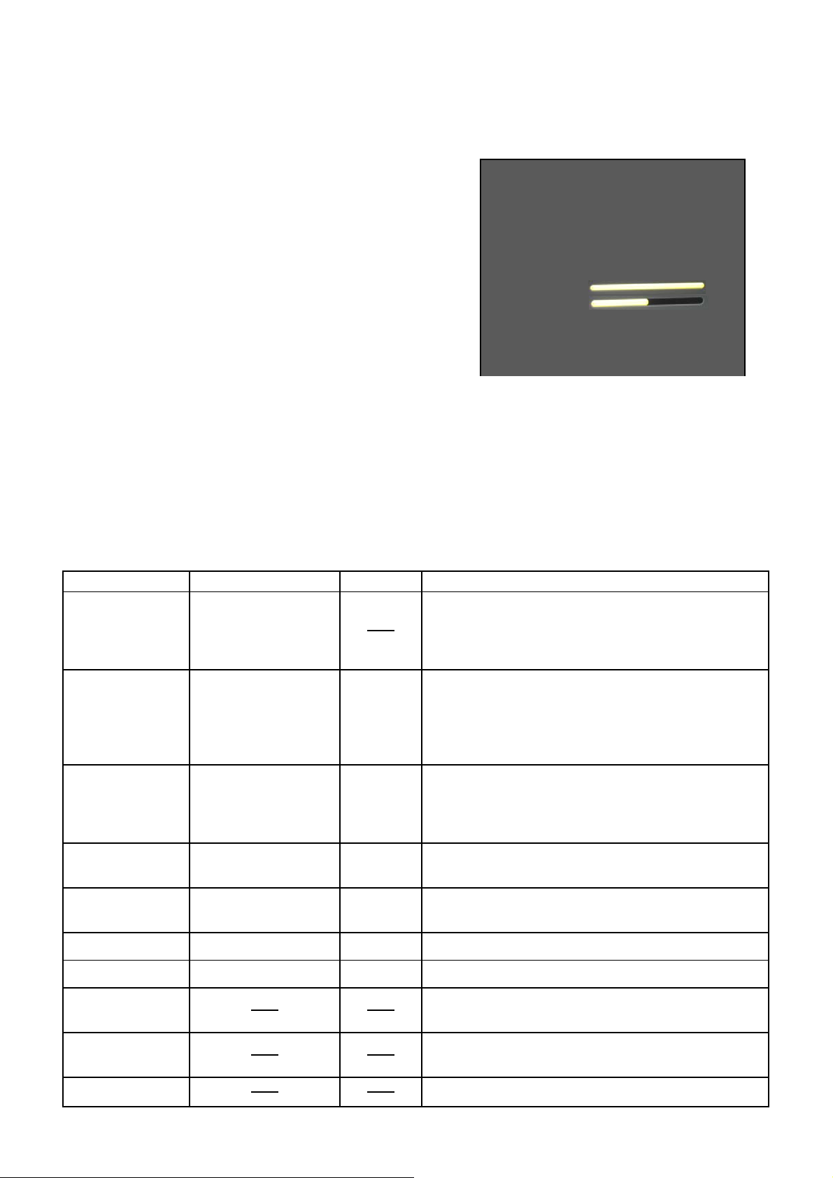
CHECK FOR THE FIRMWARE VERSION
This unit is provided with the following SERVICE MODES so you can repair, examine and adjust easily.
CAUTION
Do not adjust after other items except "Version Info".
1. Check of the VERSION and SUM DATA on the screen.
1-1 : Press the MENU ---> 1147 button on the remote control.
1-2 : Press the DOWN button on the remote control,
1-3 : Select the "Setup" menu , then press ENTER button.
1-4 : Select the "Version Info" menu, then press ENTER button.
1-5 :
On the screen as shown in Fig. 1-1.
Version : IDTV0801_002114_8_001_87
OUl Code : 0x000C3B
H/W Model ID : 0x0D27
H/W Version ID : 0x0001
S/W Model ID : 0x0D27
S/W Version ID : 0x0001
Check sum : 1EF9
Serial Number : 2012-07-26 14:34:38
Fig. 1-1
C-1
Page 16

ELECTRICAL ADJUSTMENTS
1. ADJUSTMENT PROCEDURE
Prepare the following measurement tools for electrical
2. BASIC ADJUSTMENTS
2-1: WHITE BALANCE
adjustments.
1. Place the set in Aging Test for more than 15 minutes.
1. Pattern Generator 2. Please select input About mode to adjust W/B.
3. Receive the gray scale pattern from the Pattern
On-Screen Display Adjustment
Generator.
4. Press the INPUT SELECT button on the remote control
1. Press the MENU ---> 1147 button on the remote to set to the AV mode.
control. 5. Using the remote control, set the brightness and
2. Press the DOWN button on the remote control. contrast to normal position.
3. Select the "Video" menu, then press 6. Press the MENU ---> 1147 button on the remote control.
ENTER button on the remote control. 7. Press the DOWN button on the remote control.
4. Select the "Color Temperature" menu , then press 8. Select the "Video" menu, then press
ENTER button on the remote control. ENTER button on the remote control.
5.
On the screen as shown in Fig. 1-1.
9. Select the "Color Temperature" menu , then press
ENTER button on the remote control.
10. Press the UP/DOWN button on the remote control
to select the "R Gain", "G Gain", "B Gain", "R Offset",
Color Temperature Cool
<>
"G Offset", "B Offset.
11. Adjust the LEFT/RIGHT button on the remote control
R Gain -37
G Gain 0
B Gain 102
R Offset -2
G Offset 0
B Offset -1
to whiten the R Gain, G Gain, B Gain, R Offset, G Offset,
B Offset at each step tone sections equally..
12. Perform the above adjustments 10 and 11 until the white
color is achieved.
Fig 1-1
D-1
Page 17

ELECTRICAL ADJUSTMENTS
3. ELECTRICAL ADJUSTMENT PARTS LOCATION GUIDE (WIRING CONNECTION)
LCD PANEL
CD2801
SPEAKER
CD301
CN9
CN13
CN18
CN23
CN7
CN4
CN17
CN15
CN6
MAIN UNIT
T1
CN2CN5
CN11
CN16
CN3
CP7003
CP7001
CP7002
BACK LIGHT PCB
POWER PCB
CP502
CP503
CD2202
CP2202
OPERATION PCB
CD2201
CP2201
OS2201
REMOCON PCB
CP501
AC IN
CD501
D-2
Page 18

A
)
A
C
【
HDMI-3
】
(
)
r
e
(ST)
BLOCK DIAGRA M
(
)
DVB-T/C/S/S2 Model Only DVD Combo Model Only
<Remonon PCB> <Operation PCB> <DVD PCB>
DVB-S/S2 TUNER S/S2 Demod
GAIA-20R (GOSPELL)
VL6211 (AVAILINK)
MPEG/SCALER
MT5310 (MEDIATEK
DVB-T/C TUNER
TDTK-G941D (LG) LVDS
PCMCI
TS
Bus
DEMOD.
BUS SW
MT5135AE
(MTK)
Y/Pb/PrL/R
HDMI SW I
IT6633E
<LCD PANEL>
【HDMI-1】
【HDMI-2】
SPI FLASH 64Mbit
EN25Q64-104HIP
EON
Mini 【AV1/AV】
CVBS, AUDIO L/R
Mini 【AV2/Component】
Y, Pb, P
USB
USB
Side
FUSE STA333W
5V
SPDIF Out
(Coaxial) Side
HP AMP
(OP AMP)
HP Jack
Sound AMP
Main Speak
10W + 10W
DDR3-1333 1Gb
NT5CB64M16DP-CF
NANYA
E-1
E-2
Page 19

PRINTED CIRCUIT BOARDS
POWER (INSERTED PARTS)
SOLDER SIDE
IC505
C540_1
R530
R542
W813
T502
IC502
W004
503
H
S
C536_1
D527
R509
D525
HS525
W001
D526
C531
R537
W804
S
H
5
0
4
CP502
W023
W007
W827
W003
C543
D539
W019
IC504
W808
W013
W014
C532
W012
W024
IC506
W020
W809
W021
W821
IC503
R597
W002
CEM842A
CP503
D531
IC507
D530
W825
W006
B504
R
5
3
4
R524
R536
W810
C528
C533_1
B503
R518
D519
C522_1
W005
C515
R514_1
R
5
1
5
T501_1
W009
W016
R519
D515
C517
Q501
D512
D516
C518_1
W010
C519_2
D508
B501
W018
-REPLACEASMARKED.
RISKOFFIRE
HS501
D514
D513
R508
F501
C504
W015
D510
W008
C509
D518
D517
SH502
CP501
C505
L501
C510
TH501
D511
SH501
POWER (CHIP MOUNTED PARTS)
SOLDER SIDE
R521
R522
R525
CEM842A
Q503
D507
R511
IC501
R504
R505
R507
R506
C506
C503
R512_1R513
C502
R501
C501
R503
W801
R575
R565
R571
R572
R576
C526
R523
C524
D521
C525
C534
B502
R531
D522
C527
D524
C529
C530
R529
R532 R570
R540
R543
R548
R538
R539
R567
R566
R560
Q509
R552
R551
Q506
R546
R550
R549
W807
W806
D502
Q508
R564
C547
R569
C544
C545
R558
R553
R557
R556
C549
C548_1
C551
F-1
F-2
Page 20

PRINTED CIRCUIT BOARDS
OPERATION (INSERTED PARTS)
SOLDER SIDE
SW2204
SW2202
CEM844A
SW2205
SW2206
SW2201
SW2203
CP2202
REMOCON (INSERTED PARTS)
SOLDER SIDE
CEM846A
D2201
CP2201
OS2201
OPERATION (CHIP MOUNTED PARTS)
SOLDER SIDE
C2202_1
C2201_1
R2202
R2201
R2204
CEM844A
R2203
REMOCON (CHIP MOUNTED PARTS)
SOLDER SIDE
R2210
R2209
C2203
R2208
C2204
CEM846A
BACK LIGHT (INSERTED PARTS)
SOLDER SIDE
CP7002CP7003
R7036
R7034
R7024
R7023
R7026
IC7001
C7004 R7005
R7006
C7008
C7009
R7022
R7010
R7012
C7010
R7011
C7007
R7013
R7014
R7015
R7016
R7017
C7002_1
R7037
C7033
C7032
C7031
CP7001
R7002
R7001
R7004
R7003
C7026
C7001
C7003_1
C7030
C7029
L7001
R7038
B7001
C7036
C7035
R7032
R7033
D7009
Q7001
R7029
C7027
W803
R7030
R7021
W804
W811
W810
R7018
CEM855A
R7025
HS501
BACK LIGHT (CHIP MOUNTED PARTS)
SOLDER SIDE
C7014
C7015
CEM855A
F-3 F-4
Page 21

8
7
6
5
4
3
2
CHASSIS GND
GAP_6.5mm
CP501
A3963WV2-3PD
1
GAP_6.5mm
CHASSIS GND
ABC D E F GH
EPT,FB,Vdd-GNDC
Frame GND
3
SG5013005P-R(GF-009)
5A(T) 250V
B
0.015
50V
C501
FEED BACK
F501
5A 250V
R501
CH
330P
50V
C502
PIN
D513
1N4006-A5
TH501
R504
330K
1/8W
(32-16)
R505
330K
1/8W
(32-16)
R506
330K
1/8W
(32-16)
R507
330K
1/8W
(32-16)
12M 1W RCR
R508
PRI_GND INVERTER_H
5.7
330 1/16W
1/16W
18K
R503
CH
33P
50V
C503
1234
2.8
1.8
0
LE-MX
310V
C504 0.33
SH501
SH502
YQ-12
YQ-12
POWER CONTROL
IC501
FA5640N-C6-TE3
ZCD
FB
IS
GND
COIL LINE FILTER
L501
JLB28120
12
34
21.3
VH
78
NC
NC
21.0
VCC
21.3
56
OUT
IC
GND
ICGND
W801
C505
R511
0.0015250V E
R512_1
33
100 1/16W
1/10W
D507
C506
B57237S0479M000
0.22310V LE-MX
C509
C510
D512
EC11FS2-TE12L
D508
0.1 B
0.0015250V E
SWITCHING
FMV09N90E
MTZJ33B
MTZJ33B
Q501
D515
R513
19.3 169.0
G
33K 1/16W
MTZJ33B
D
S
R519
D514
1.8
1N4006-A5
D510
ZRM11C
D511
ZRM11C
12.5mm
0.12 1W
D519
1N4006-A5
C519_2
680P2KV R
C517
FOR Q501
NC
HS501
763WAA0402
D517
ZRM11C
D518
ZRM11C
120400V 35*20mmGJ
C522_1
B501
W4BRH3.5X6X1.0
R514_1
12.5*20mm
PT
22400V
C518_1
220K 1W RCR
47P2KV SL
D516
C515
R521
1/10W
R575
2.2M
R565
2.2M 1/10W
R571
2.2M
1/10W
R572
2.2M
1/10W
R576
22K 1/10W
R515
0.22 1W
SARS02-LFB2
0.0022630V PP
R518
47 1/4W
68K 1/16W
D521 UDZSNP15B
15mm
W810
1.06 0 4.4
MIP2M40MSSCF
SUB POWER CTL
VDDLSFB VCC
IC502
1234
B
B
1
50V
C524 0.150V
C534
VCC SW
Q503
KTA1664-Y-RTF/P
T501_1 81351254
67
5
3
2
NC
1
R522
1.08 1.03
100 1/16W
1.08
UDZSNP30B
0.002250V B
D522
C526
34
PS2561AL1-1-V(W)
R523
C525
16
1
1.03
2
FEED BACK
IC507
10K 1/16W
0.2225V B
16.716.7
8
9
10
11
12
B503
W4BRH3.5X6X1.0
C533_1
47P2KV SL
578
W813
SO
6.1 17.52.16.1
C527 0.150V B
R536
10 1/4W
R524
10K 1/4W
D
C528 4750V YXF
D524 UDZSNP33B
W821
R525
B504
W4BRH3.5X6X1.0
D530
R542
1F5-E
47 1/4W
W825
D527
FCF10A20
3
2
1
For D525 and D527
HS525
763WAA0402
D525
FCF10A20
3
1
1K 1/16W
BLM31PG121SN1L
D526
FCH10A10
3
1
2
C529
0.039 B
S
NC
R534
0.22 1W
182
NC
D531
ST02D-140
158
B502
R531
4.7K 1/16W
PS2561AL1-1-V(W)
R530
2.2K 1/4W
2
C531
IC503 KIA431A-AT
SUB SW TRANS
T502 81190201
79
6
5
60
3
0
2
C540_1 0.001250V E
1.3
1.3
34
FEED BACK
IC505
0.5
0.5
34
SOFT SWITCH
KTC3875S_Y_RTK
C532 100025V 10*20mmZLJ
C536_1 100025V 10*20mmZLJ
ZLH_P
150035V
16*20mm
C530
0.00150V B
SHUNT REG IC
R537
R570
1K 1/16W
2.2K 1/16W
R529
3.3K 1/16W
1/2W
1.8K
R532
6
6
11
0
13
0
15
1.0
1
1.0
2
POWER SW
IC506
PS2561AL1-1-V(W)
1.1
1
1.1
2
R546
1
0
Q506
1K 1/16W
0.7
R548
R552
R551
4.7K 1/16W
R566
R538
R539
IS THE LIVE CONNECTIONCAUTION:
POWER SCHEMATIC DIAGRAM
(POWER PCB)
D539
FCQS10A065
1
3
R549
470 1/16W
1K 1/16W
R550
560 1/16W
R560
10K 1/16W
5.8
SHORT PROTECT
5.8
10K 1/16W
KTC3875S_Y_RTK
4.7K 1/16W
R567
1.2K
1/16W +-1%
33K
1/16W +-1%
Q508
W809
4.7K
1/16W
5.8
2
IC504
5.8
5.8
5.8
C547
R509
R543
18K 1/16W +-1%
HD
10*16mm
100010V
C543
Shunt Reg IC
KIA431A-AT
CATHODE
ANODE
4.5 0 2.4
C545
R553
0.022 B
3.3K
1/16W
C544
0.00150V B
R564
1K 1/16W
SHORT PROTECT
Q509
KTA1504S_Y_RTK
D502
UDZSNP30B
0.0150V B
10K
R569
1/16W
W808
1.8K 1/2W
R556
+-1%
910 1/16W
REFERENCE
R557
123
W804
FB_INV+24V
FB_INV+24V
+-1%
2.2K 1/16W
R558
+-1%
2.2K 1/16W
POWER_ON-H
FB_INV+24V
R597
560 1/4W
GND
SOUND+B
FB_SW+12V
SW+12V
SOUND_GND
INV_GND INVERTER_H
INV+24V
FB_SW+12V
AT+5.5V
GND
SW+12V
SOUND+B
SOUND_GND
POWER_ON-H
LIGHT_CTL
INV+24V
INV_GND
LIGHT_CTL
AT+5.5V
0.150V B
C548_1
C549
C551
GND
W807
0.150V B
0.150V
B
W827
W806
FROM/TO MAIN UNIT
(CN3)
CP502
00_6216_018_000_808+
SW+12V
SW+12V
AT+5.5V
AT+5.5V
AT+5.5V
GND
GND
GND
SW+12V/GND
SW+12V
SOUND+B
SOUND+B
SOUND_GND
SOUND_GND
POWER_ON_H
NC
POWER_FAIL
LIGHT_CTL
INVERTER_H
FFC 18pin
CD502
2H0I2801
FROM/TO BACK LIGHT
(CP7001)
A2001WV-8A
+24V
+24V
+24V
GND
GND
GND
INVERTER_H
LIGHT_CTL
P=2.0mm 8PIN
CD503
EA283301
CP503
8
7
18
17
16
15
6
14
13
12
11
10
9
8
7
6
5
4
3
5
2
1
1
4
2
3
4
5
6
7
8
3
2
1
G-1
T3.15A L250V
CAUTION
ATTENTION
CAUTION
ABC D E F GH
:FOR CONTINUED PROTECTION AGAINST FIRE HAZARD,
REPLACE ONLY WITH THE SAME TYPE FUSE
T3.15A L250V(F501)
:POUR UNE PROTECTION CONTINUE LES RISQUES D’INCEIE
N’UTILISER QUE DES FUSIBLE DE MEME TYPE
T3.15A L250V(F501)
F501 IS MANUFACTURED BY SKYGATE CO., LTD., TYPE SCT.
NOTE:THIS SCHEMATIC DIAGRAM IS THE LATEST AT THE TIME
OF PRINTING AND SUBJECT TO CHANGE WITHOUT NOTICE
NOTE:THE DC VOLTAGE AT EACH PART WAS MEASURED
WITH THE DIGITAL TESTER WHEN THE COLOR BROADCAST
WAS RECEIVED IN GOOD CONDITION AND PICTURE IS NORMAL.
16.7 0 2.4
THE RESISTOR MARKED F IS FUSE RESISTOR.NOTE:
THE ALUMI ELECTROLYTIC CAPACITOR MARKED NP
IS NON POLAR ONE.
CATHODE
REFERENCE
ANODE
123
ATTENTION
R540
2.2K 1/16W +-1%
:LES PIECES REPAREES PAR UN ETANT
DANGEREUSES AN POINT DE VUE SECURITE
N’UTILISER QUE CELLS DECRITES
DANS LA NOMENCLATURE DES PIECES
SH503
YQ-12
SH504
YQ-12
GND
CAUTION
PCB240
CEM842
:SINCE THESE PARTS MARKED BY
CRITICAL FOR SAFETY,USE ONES
DESCRIBED IN PARTS LIST ONLY
1
ARE
G-2
Page 22

ABC D E F GH
OPERATION/REMOCON SCHEMATIC DIAGRAM
8
OS2201
7
6
KSM-2003TCW2P
1
Vout
GND
2
B+
3
C2204
R2208
47 1/16W
B
B
22
22
C2203
6.3V
6.3V
(OPERATION/REMOCON PCB)
(REMOCON PCB)
R2209
330 1/16W
R2210
330 1/16W
3
STANDBY/POWER
G
R
D2201
LTL-1BEFJ-002A
12
GND4
FROM/TO MAIN UNIT
CP2201
(CN2,CN6)
A2001WR-5A
REMOCON IN
GND
AT+5VAT+3.3V
STANDBY LED
POWER ON LED
CD2201
CH253602
1
2
3
4
5
PCBDA0
CEM846
5
8
7
6
5
(OPERATION PCB)
4
B
CH+
SW2201
3
EVQ21505R
R2201
12K 1/16W
VOL-
SW2202
EVQ21505R
R2202
6.8K 1/16W
SW2203
INPUT/ENTER
EVQ21505R
R2203
3.9K 1/16W
POWER
SW2204
EVQ21505R
VOL+
SW2205
EVQ21505R
R2204
56K 1/16W
CH-
SW2206
EVQ21505R
C2201_1
B
C2202_1
0.1
0.1
KEY-B
KEY-A
FROM/TO MAIN UNIT
(CN5)
CP2202
A2001WR-3A
GND
KEY B
KEY A
CD2202
CH243901
1
2
3
PCB270
CEM844
2
4
3
2
NOTE:THIS SCHEMATIC DIAGRAM IS THE LATEST AT THE TIME
1
OF PRINTING AND SUBJECT TO CHANGE WITHOUT NOTICE
NOTE:THE DC VOLTAGE AT EACH PART WAS MEASURED
WITH THE DIGITAL TESTER WHEN THE COLOR BROADCAST
WAS RECEIVED IN GOOD CONDITION AND PICTURE IS NORMAL.
1
ABC D E F GH
G-4G-3
Page 23

8
7
6
5
4
3
FROM/TO POWER
CP7001
A2001WR-8A
1
VBL(+24V)
2
VBL(+24V)
3
VBL(+24V)
4
GND
5
GND
GND
6
7
BLON
8
PWM
ABC D E F GH
BACK LIGHT SCHEMATIC DIAGRAM 1
(CP503)
C7001
C7002_1
B
0.150V
0.00150V B
(1608)
C7003_1
100 1/16W
0.00150V B
R7001
R7002
100 1/16W
R7003
22K 1/16W
R7004
VIN_24V
22K 1/16W
PWM
(BACK LIGHT PCB)
C7029
470P50V CH
W804
L7001
33uH
B966BS
C7027
DRIVE
24.7
Q7001
D
1.7
RSD050N10
G
S
0
100P50V CH
+-1%
+-1%
R7029
R7030
(2125)
0.1 1/4W
0.1 1/4W
EN
VIN_24V
W803
(1608)
B
C7026 0.150V
P_GND
C7014
AGND
UVLO
LSP
RT
FB
SS
CP
VREF
S1
S2
S3
S4
S5
S6
S7
S8
PWM8
PWM7
PWM6
2.250V (3216)B
LED DRIVER
35
VCC
FAIL
VREG
PGND
OVP
STB
LED1
LED2
LED3
LED4
LED5
LED6
LED7
LED8
PWM1
PWM2
PWM3
PWM4PWM5
23.6
110111213141516171819 220
R7025
5
100K 1/16W
5
3
1.7
4
N
56789
0
CS
1.8
3
9
9
9
9
9
9
3
3
3
3
C7015
4.710V
(2125)
R7026 10 1/16WR7012 100K 1/16W +-1%
B
HS501
763WSA0073
A_GND
GND
EN
PWM
R7005 47K 1/16W +-1%
R7006 10K 1/16W +-1%
C7004 0.110V B
R7010 180K 1/16W +-1%
C7007 0.116V
C7008 0.016.3V B
C7009 0.476.3V B
R7011 470K 1/16W +-1%
C7010 0.110V B
R7013 1.5 1/4W (2125)+-1%
R7014 1.5 1/4W (2125)+-1%
R7015 1.5 1/4W (2125)+-1%
R7016 1.5 1/4W (2125)+-1%
R7017 1.5 1/4W (2125)+-1%
R7018 1.5 1/4W (2125)+-1%
W810
W811
R7021 10 1/16W
B
(1005)
R7022
240 1/16W
IC7001 BD8779EFV-E2
40
2.6
NC
4.5
0.1
0.1
0.1
1
0.1
0.1
0.1
30 31 32 33 34 35 36 37 38 39
0.1
0.1
0.1
0
0
0
0
23 24 25 26 27 28 29
3.0
3
21 22
D7009
SK3BA
(2125)
C7030
470P50V CH
C7031 100V0.1100V (1608)X7R
C7032 100V0.1100V (1608)X7R
CASE OF SILVER THROUGHT PCB,
THAT PATTERN IS CONNECTED USING THROUGHT-HOLEIT IS NG,
B7001
HCB3216KF-391T20
R7032
680K 1/16W +-1%
0.00150V B
C7035
C7033 27063V ZLJ
R7033
C7036
33K 1/16W +-1%
0.00150V B
R7023 4.7 1/4W +-1%
R7024 4.7 1/4W +-1%
R7034 4.7 1/4W +-1%
R7036 4.7 1/4W +-1%
R7037 4.7 1/4W +-1%
R7038 4.7 1/4W +-1%
NC
NC
CP7002
FCZ100E-07SS-K
LED1
LED2
LED3
LED7/NC
NC
VLED
VLED
CP7003
FCZ100E-07SS-K
LED4
LED5
LED6
LED8/NC
NC
VLED
VLED
1
2
3
4
5
6
7
1
2
3
4
5
6
7
8
7
6
5
4
3
2
PCB350
CEM855
NOTE:THIS SCHEMATIC DIAGRAM IS THE LATEST AT THE TIME
1
OF PRINTING AND SUBJECT TO CHANGE WITHOUT NOTICE
THE RESISTOR MARKED F IS FUSE RESISTOR.NOTE:
THE ALUMI ELECTROLYTIC CAPACITOR MARKED NP
IS NON POLAR ONE.
NOTE:THE DC VOLTAGE AT EACH PART WAS MEASURED
WITH THE DIGITAL TESTER WHEN THE COLOR BROADCAST
WAS RECEIVED IN GOOD CONDITION AND PICTURE IS NORMAL.
CAUTION
:SINCE THESE PARTS MARKED BY
CRITICAL FOR SAFETY,USE ONES
DESCRIBED IN PARTS LIST ONLY
ARE
ATTENTION
:LES PIECES REPAREES PAR UN ETANT
DANGEREUSES AN POINT DE VUE SECURITE
N’UTILISER QUE CELLS DECRITES
DANS LA NOMENCLATURE DES PIECES
2
1
ABC D E F GH
G-6G-5
Page 24

ABC D E F GH
INTERCONNECTION DIAGRAM
8
P=2.0mm 8PIN
CP7002
LED1
1
LED2
2
LED3
3
LED7/NC
4
5
VLED
6
VLED
7
NC
NC
NC
7
CP7003
LED4
1
LED5
2
LED6
3
LED8/NC
4
5
VLED
6
VLED
7
NC
NC
NC
VBL(+24V)
VBL(+24V)
VBL(+24V)
GND
GND
GND
BLON
PWM
BACK LIGHT PCB
PCB350
CEM855
CP7001
CD503
CP503
1
1
2
2
3
3
4
4
5
5
6
6
7
7
8
8
+24V
1
1
+24V
2
2
+24V
3
3
GND
4
4
GND
5
5
GND
6
6
INVERTER_H
7
7
LIGHT_CTL
8
8
NC
SW+12V
SW+12V
AT+5.5V
AT+5.5V
AT+5.5V
GND
GND
GND
SW+12V/GND
SW+12V
SOUND+B
SOUND+B
SOUND_GND
SOUND_GND
POWER_ON_H
POWER_FAIL
LIGHT_CTL
INVERTER_H
CP502
CD3003
CN3
SW+12V
18
18
17
17
16
16
15
15
14
14
13
13
12
12
11
11
10
10
9
9
8
8
7
7
6
6
5
5
4
4
3
3
2
2
1
1
1
18
17
16
15
14
13
12
11
10
SW+12V
2
AT+6.0V
3
AT+6.0V
4
AT+6.0V
5
6
GND
GND
7
GND
8
SW+12V
9
SW+12V
9
10
SOUND+18V
8
11
SOUND+18V
7
12
6
5
4
3
2
1
GND
13
GND
14
PW_ON
15
16
ADJ
17
BL_ON
18
6
CD501
CP501
21
1
BROWN
3
BLUE
5
OS2201
Vout
1
GND
2
TM101
B+
3
COMMAND TRANSMITTER
STANDBY/POWER
D2201
3
G
R
1 2
POWER PCB
PCB240
CEM842
REMOCON IN
GND
AT+5VAT+3.3V
STANDBY LED
POWER ON LED
REMOCON PCB
PCBDA0
CEM846
CP2201
CD6201
1
1
2
2
3
3
4
4
5
5
CN6
IR
1
1
GND
2
2
3
3
+3V3_STB
1
4
LED_R
5
2
GND
3
LED_G
CN2
4
CD6207
CP2202
GND
KEY B
KEY A
OPERATION PCB
PCB270
CEM844
1
1
2
2
3
3
CN5
+3V3_TOUCH
1
3
2
2
3
1
4
GND
3
2
1
CN23
1
2
3
4
5
6
4
3
2
1
10
11
12
13
14
15
16
17
18
19
CN4
CN18
1
2
3
4
5
6
7
8
9
8
234
7
OUTL+
OUTL-
OUTR-
OUTR+
HDMI1_RX2+
GND
HDMI1_RX2HDMI1_RX1+
GND
HDMI1_RX1-
HDMI1_RX0+
GND
HDMI1_RXCHDMI1_RXC+
GND
HDMI1_RXC-
CEC
RX5V1 DDC SCL
RX5V1 DDC SDA
GND
HDMI1 5VIN
RX1_HOTPLUG/
5
CN13
CN15
1
HDMI1_RX2+
2
3
HDMI1_RX2-
4
HDMI1_RX1+
5
HDMI1_RX1-
6
HDMI1_RX0+
7
8
GND
9
HDMI1_RXCHDMI1_RXC+
10
11
HDMI1_RXC-
12
CEC
13
14
RX5V1 DDC SCL
15
RX5V1 DDC SDA
16
17
GND
HDMI1 5VIN
18
RX1_HOTPLUG/
19
CN17
1
HDMI1_RX2+
2
3
HDMI1_RX2-
4
HDMI1_RX1+
5
HDMI1_RX1-
6
HDMI1_RX0+
7
8
GND
9
HDMI1_RXCHDMI1_RXC+
10
11
HDMI1_RXC-
12
CEC
13
14
RX5V1 DDC SCL
15
RX5V1 DDC SDA
16
17
GND
HDMI1 5VIN
18
RX1_HOTPLUG/
19
GND
GND
GND
GND
GND
GND
CN19
1
2
3
4
5
6
7
8
9
10
11
12
13
14
15
16
17
18
19
20
21
22
23
24
25
26
27
28
29
30
10
11
12
13
14
15
16
17
18
19
20
21
22
23
24
25
26
27
28
29
30
CN11
1
2
3
4
5
6
7
8
9
WPN1
100ohm
GND
TX AO0N
TX AP0P
GND
TX AO1N
TX AO1P
TX AO2N
TX AO2P
TX AOCKN
TX AOCKP
TX AO3N
TX AO3P
VCC-Panel
VCC-Panel
VCC-Panel
VCC-Panel
VCC-Panel
TX AE0N
VCC-Panel
VCC-Panel
GND
TX AE2P
TX AE1P
TX AE1P
VCC-Panel
VCC-Panel
GND
GND
GND
GND
WPN2
GND
GND
GND
TX AE3N
TX AECKN
TX AO3N
TX AOCKKP
GND
TX AO2N
TX AO1P
GND
TX AO0N
TX AE2N
TX AE1N
TX AE3P
TX AECKP
TX AO3P
GND
TX AOCKN
TX AO2P
GND
TX AO1N
TX AO0P
GNDgnd
DVD_COAX
GND
DVD EM
DVD KEY
DVD_MUTE/
GND
DVD_R_IN
GND
DVD L IN
GND
DVD Y
DVD C
GND
DVD RESET/
GND
START_SW/
GND
DVD TXD/
DVD RXD/
GND
SW_+12V
GND
GND
GND
AT+6.0V
AT+6.0V
MAIN UNIT
MAIN001
CN16
CN12
1
2
3
4
5
6
7
8
9
10
11
12
13
14
15
16
17
18
19
20
21
22
23
24
1
2
3
4
5
6
8
7
6
5
4
3
2
NOTE:THE DC VOLTAGE AT EACH PART WAS MEASURED
1
WITH THE DIGITAL TESTER WHEN THE COLOR BROADCAST
WAS RECEIVED IN GOOD CONDITION AND PICTURE IS NORMAL.
ATTENTION
:LES PIECES REPAREES PAR UN ETANT
DANGEREUSES AN POINT DE VUE SECURITE
N’UTILISER QUE CELLS DECRITES
DANS LA NOMENCLATURE DES PIECES
1
ABC D E F GH
G-8G-7
Page 25

SCALER VIDEO/AUDIO
PR
AUDIO OUT L
20us 200mv
500mv 2ms
AV IN PC AUDIO L
200mv
10us 200mv
PY PC AUDIO R
100mv 500mv
10us 1ms
2ms
WAVEFORMS
200mv 500mv
10us 1ms
PB AUDIO OUT R
200mv 2v
1ms 1ms
AU AUDIO IN L SPEAKER L
200mv 2v
1ms 1ms
AU AUDIO IN R
SPEAKER R
NOTE:
Main Board Signal Input/Output.
H-1
Page 26

102B
207
102A
109
MECHANICAL EXPLODED VIEW
111
207
205
207
105
201
102
208
104C
104
201
206
104E
105
208
104D
201
204
104A
208
104C
105
206
104D
208
104E
104B
110
103B
103A
103
103B
103B
103B
103B
101D
101
101F
(POWER PCB ASS'Y)
PCB240
101E
101H
101A
101C
101G
101B
101B
203
202
101D
203
203
202
203
(BACK LIGHT PCB ASS'Y)
PCBDA0
(REMOCON PCB ASS'Y)
Note : SCREW TAP TITE(B) BIND 3x6 CH 2 PCS. (209)
is included in LED MODULE ASS'Y (SCREW).
PCB350
108
209209
108
MAIN001
(MAIN UNIT)
203
203
107
PCB270
(OPERATION PCB ASS'Y)
203
106
I-1
I-2
Page 27

MECHANICAL REPLACEMENT PARTS LIST
REF. NO. PART NO. DESCRIPTION
101 7A7080093B FRONT CABI ASS'Y
101A 708WPD0070 CABINET FRONT
101B 713WPA0478 GLASS LED
101C 800WQ00190 FELT SHEET
101D 92P20A005A CUSHION BEZEL LR
101E 93P20A017A CUSHION BEZEL
101F 93P20A024A CUSHION BEZEL TB
101G 93P30A011A TAPE
101H 93P300065A TAPE
102 7A702B743A COVER BACK ASS'Y
102A 702WPAC062 COVER BACK
102B 722202B598 SHEET RATING
103 7A704A456B STAND ASS'Y
103A 704WPAA317 STAND
103B 800WFAA082 CUSHION LEG
104 7A709A018A SPEAKER BOX ASS'Y
104A 709WPA0077 SPEAKER BOX
104B 721000A136 SHEET BUTTON
104C 800WF0A031 CUSHION SPEAKER
104D 800WQ0A252 FELT SHEET
104E 800WQ0A322 FELT SHEET
105 800CR00001 DAMPER SPEAKER
106 723000G016 SHEET JACK 1
107 761WSAA511 PLATE JACK
108 709WPA0051 HOLDER WIRE
109 769WSA0022 VESA SHAFT
110 704WPA0211 STAND FRAME or
704WPAA343 STAND FRAME
111 722000A910 HELP LINE LABEL
201 8109D30A0U SCREW TAP TITE(B) WH8 3x10
202 8109I30A0U SCREW TAP TITE(B) WH7 3x10
203 810923080U SCREW TAP TITE(B) BIND 3x8
204 810B150C0S SCREW WASHER(B) M5x30
205 8109230A0S SCREW TAP TITE(B) BIND 3x10
206 810923060S SCREW TAP TITE (B)BIND 3x6
207 810923080S SCREW TAP TITE(B) BIND 3x8
208 811022680S SCREW TAP TITE(P)BIND 2.6x8
209 810923060U SCREW TAP TITE(B) BIND 3x6
----- 723000G017 ENERGY LABEL
--- 723000G018 SHEET CARTON
--- 791WHAA396 FILM BAG
--- 791WHAA503 GIFT SHEET
--- 791WHAA508 LAMIFILM BAG
--- 792PHAA129 PACKAGE TOP
--- 792PHAA130 PACKAGE BOTTOM
--- 793PCDA496 GIFT BOX
--- 7G8900007A SCREW ASS'Y
--- J3NW0101A INSTRUCTION BOOK(DE)
--- J3NW0110A INSTRUCTION BOOK(FR)
--- J3NW0111A INSTRUCTION BOOK(PL)
--- J3NW0114A INSTRUCTION BOOK(EN)
--- JB5PD000 POLYBAG INSTRUCTION(RED CAUTION)
J1-1
Page 28

ELECTRICAL REPLACEMENT PARTS LIST
REF. NO. PART NO. DESCRIPTION REF. NO. PART NO. DESCRIPTION
RESISTORS COILS &TRANSFORMERS
! R504 R8X2R8334J RC 330K OHM 1/8W ! T501 0481351254 TRANSFORMER,SWITCHI NG 81351254
! R505 R8X2R8334J RC 330K OHM 1/8W ! T502 0481190201 TRANSFORMER,SWITCHI NG 81190201
! R506 R8X2R8334J RC 330K OHM 1/8W
! R507 R8X2R8334J RC 330K OHM 1/8W J101 060R412002 RCA JACK RCA/RGB-12329-02
! R508 RC31X1126J RC 12M OHM 1W
! R513 R803R9333J RC 33K OHM 1/16W SW2201 0504101T34 SWITCH,TACT EV Q21505R
! R514 RC31X1224J RC 220K OHM 1W SW2202 0504101T34 SWITCH,TACT EVQ21505R
! R515 R63881R22J R,FUSE 0.22 OHM 1W SW2203 0504101T34 SWITCH,TACT EVQ21505R
! R518 R65584470J R,FUSE 47 OHM 1/4W SW2204 0504101T34 SWITCH,TACT EVQ21505R
! R519 R3K781R12J R,META L OXIDE 0.12 OHM 1W S W2205 0504101T34 SWITCH,TACT EVQ21505R
! R534 R63881R22J R,FUSE 0.22 OHM 1W SW2206 0504101T34 SWITCH,TACT EVQ21505R
JACKS
SWITCHES
CAPACITORS P.C.BOARD ASSEMBLIES
! C501 CS0PB04E4K CC 0.015 UF 50V B PCB240 A3MW01W240P POWER PCB ASS'Y CEM842A
! C502 CS0PCH4L2J CC 330 PF 50V CH PCB270 A3MW01W270P OPERATION PCB ASS'Y CEM844A
! C503 CS0PCH4L1J CC 33 PF 50V CH PCB350 A3MW01W350P BACK LIGHT PCB ASS'Y CEM855A
! C504 P4K12D334K CMPP 0.33 UF 310V PCBDA0 A3MW01WDA0P REMOCON PCB ASS'Y CEM846A
! C505 CE39E0ME3M CC 1 0.0015UF 250V E
! C506 CS0PB0415K CC 0.1 UF 50V B B501 024HT03564 CORE,B EADS W4BRH3.5X6X1.0
! C509 P4K12D224K CMPP 0.22 UF 310V ! B502 024AC1121G CORE,BEADS BLM31PG121SN1L
! C510 CE39E0ME3M CC 0.0015UF 250V E B 503 024HT03564 CORE,BEADS W4BRH3.5X6X1.0
! C515 P3N5F5222J CPP 0.0022UF 630V PP B504 024HT03564 CORE,B EADS W4BRH3.5X6X1.0
! C517 C0PLRR7U2K CC 680 PF 2KV R B7001 024HC13914 CORE,BEADS HCB3216KF-391T20
C518 CP3YSL7Q1J CC 47 PF 2KV SL BT001 141U004021 BATTERY,M ANGAN AAA(R03)
! C519 E83FHH121D CE 120 UF 400V BT002 141U004021 BATTERY,MANGAN AAA(R03)
! C522 E63ZFH220D CE 22 UF 400V CD301 06EH144602 CORD CONNECTOR EH144602
! C528 E8E2U5470D CE 47 UF 50V ! CD501 120A658806 CORD AC BUSH MO27-020BK
! C531 E8E1G4152M CE 1500 UF 35V CD502 122H0I2801 CORD JUMPER 2H0I2801
! C532 E9E8F3102D CE 1000 UF 25V CD503 06EA283301 CORD CONNECTOR EA283301
! C533 CP3YSL7Q1J CC 47 PF 2KV SL CD505 06EHB18006 CORD,RCA PIN CRM0318002
! C536 E9E8F3102D CE 1000 UF 25V ! CP501 069S320419 CONNECTOR P CB SIDE A3963WV2-3PD
C540 CE39E0M13M CC 0.001 UF 250V E CP502 069E 7I0630 CONNECTOR PCB SIDE 00_6216_018_000_808+
! C543 E83YT1102D CE 1000 UF 10V CP503 06GG280029 CONNECTOR PCB SIDE A2001WV-8A
C7033 E9E806271D CE 270 UF 63V CD2201 06CH253602 CORD CONNECTOR CH253602
DIODES
D502 DE7RB3002B DIODE ZENER UDZSNP30B TE-17 CP2201 06GG250019 CONNECTOR PCB SIDE A2001WR-5A
D507 D28R11FS 20 DIODE EC11FS2-TE12L CP2202 06GG230019 CONNECTOR PCB SIDE A2001WR-3A
! D508 D97U03301B DIODE,ZENER MTZJ33B T-77 CP7001 06GG280019 CONNECTOR PCB SIDE A2001WR-8A
! D510 D4JXRM11C0 DIODE SILICON ZRM11C CP7002 06GRV73019 CONNECTOR PCB SIDE FCZ100E-07SS-K
! D511 D4JXRM11C0 DIODE SILICON ZRM11C CP7003 06GRV73019 CONNECTOR PCB SIDE FCZ100E-07SS-K
! D512 D97U03301B DIODE,ZENER MTZJ33B T-77 EL2401 124116281A EYE LET EYE LET XRY16X28BD
! D513 D4CTN40060 DIODE SILICON 1N4006-A5 EL2402 124120301A EYE LET EYE LET XRY20X30BD
! D514 D4CTN40060 DIODE SILICON 1N4006-A5 ! F501 0805A05003 FUSE SG5013005P-R(GF-009)
! D515 D97U03301B DIODE,ZENER MTZJ33B T-77 MAIN001 1564200017 MAIN UNIT T.MT5310.S97A_TC
! D516 D2BFARS020 DIODE SILICON SARS02-LFB2 OS2201 077Q038009 REMOTE RECEIVER KSM-2003TCW2P
! D517 D4JXRM11C0 DIODE SILICON ZRM11C SH501 126D000045 TERMINAL PI N YQ-12
! D518 D4JXRM11C0 DIODE SILICON ZRM11C SH502 126D000045 TERMINAL PI N YQ-12
! D519 D4CTN40060 DIODE SILICON 1N4006-A5 S H503 126D000045 TERMINAL PIN YQ-12
D521 DE7RB1502B DIODE ZENER UDZSNP15B TE-17 SH504 126D000045 TE RMINAL PIN YQ-12
D522 DE7RB3002B DIODE ZENER UDZSNP30B TE-17 ! SP301 070Y056014 SPEAKER S0412F41
D524 DE7RB3302B DIODE ZENER UDZSNP33B TE-17 ! SP302 070Y056014 SPEAKER S0412F41
! D525 D28A10A200 DIODE SILICON FCF10A20 ! TH501 DSVEHE4R7M THERMISTOR B57237S0479M000
! D526 D28A10A100 DIODE SCHOTTKY BARRIER FCH10A10 TM101 076D0UE071 TRA NSMITTER 000-225000070
! D527 D28A10A200 DIODE SILICON FCF10A20 TU001 0164E03021 DIGITAL TUNE R TDTK-G731D(A)
D530 D2LT001F50 DIODE SILICON 1F5-E ! V2801 A3MW01WFM0P LED MODULE ASS'Y V290BJ1-P E1-LED OR1
! D531 DK1T2D1400 POWER CLAMPER ST02D-140
! D539 D28A10A061 DIODE SCHOTTKY BARRIER FCQS10A 065
D2201 0021E9Q010 LED LTL-1BEFJ-002A RESISTOR
! D7009 D4CRSK3BA0 DIODE SCHOTTKY BARRIE R SK3BA RC................... CARBON RESISTOR
CD2202 06CH243901 CORD CONNECTOR CH243901
MISCELLANEOUS
ICS
IC501 ICAJ0A5640 POWER IC CONTROL FA5640N-C6-TE3 CAPACITORS
! IC502 I5SD0P2M40 VDSS=700V F=67KHZ MIP2M40MSSCF CC................... CERAMIC CAPACITOR
! IC503 I1KJ9A431A VARIABLE SHUNT REGULATOR TAPE KIA431A-AT CE................... ALUMI ELECTROLYTIC CAPACITOR
! IC504 I1KJ9A431A VARIABLE SHUNT REGULATOR TAPE KIA431A-AT CP................... POLYESTER CAPACITOR
! IC505 000220002W PHOTO COUPLER PS2561AL1-1-V(W) CPP.................. POLYPROPYLENE CAPACITOR
! IC506 000220002W PHOTO COUPLER PS2561AL1-1-V(W) CPL.................. PLASTIC CAPACITOR
! IC507 000220002W PHOTO COUPLER PS2561AL1-1-V(W) CMP................ METAL POLYESTER CAPACITOR
! IC7001 I07F087790 LED DRIVER IC BD8779EFV-E 2 CMPL................ METAL PLASTIC CAPACITOR
TRANSISTORS
! Q501 TK1009N900 FET FMV09N90E
! Q503 TA AA01664Y TRANSISTOR SILICON KTA1664-Y-RTF/P
Q506 TCAA3875SY TRANSISTOR SILICON KTC3875S_Y_RTK
Q508 TCAA3875SY TRANSISTOR SILICON KTC3875S_Y_RTK
Q509 TAAA1504SY TRANSISTOR SILICON KTA1504S_Y_RTK
! Q7001 TJ7T50N100 FET RSD050N10TL
CMPP................ METAL POLYPROPYLENE CAPACITOR
COILS &TRANSFORMERS
! L501 029B000185 COIL, LINE FILTER JLB28120
L7001 021YM5330M COIL 33 UH
J2-1
Page 29

SPEC.NO. M3MW-01W
O/R NO. F2X3214
 Loading...