

Page 1
查询NTB45N06供应商
NTP45N06, NTB45N06
Power MOSFET
45 Amps, 60 Volts
N–Channel TO–220 and D2PAK
Designed for low voltage, high speed switching applications in
power supplies, converters and power motor controls and bridge
circuits.
Features
• Higher Current Rating
• Lower R
• Lower V
• Lower Capacitances
• Lower Total Gate Charge
• Tighter V
• Lower Diode Reverse Recovery Time
• Lower Reverse Recovery Stored Charge
T ypical Applications
• Power Supplies
• Converters
• Power Motor Controls
• Bridge Circuits
MAXIMUM RATINGS (T
Drain–to–Source Voltage V
Drain–to–Gate Voltage (RGS = 10 MΩ) V
Gate–to–Source Voltage
Drain Current
Total Power Dissipation @ TA = 25°C
Total Power Dissipation @ TA = 25°C (Note 1.)
Total Power Dissipation @ TA = 25°C (Note 2.)
Operating and Storage Temperature Range TJ, T
Single Pulse Drain–to–Source Avalanche
1. When surface mounted to an FR4 board using 1″ pad size,
(Cu Area 1.127 in2).
2. When surface mounted to an FR4 board using the minimum recommended
pad size, (Cu Area 0.412 in2).
DS(on)
DS(on)
Specification
SD
= 25°C unless otherwise noted)
J
Rating Symbol Value Unit
– Continuous
– Non–Repetitive (tp10 ms)
– Continuous @ TA = 25°C
– Continuous @ TA = 100°C
– Single Pulse (tp10 µs)
Derate above 25°C
Energy – Starting TJ = 25°C
(VDD = 50 Vdc, VGS = 10 Vdc, RG = 25 Ω,
I
= 40 A, L = 0.3 mH, VDS = 60 Vdc)
L(pk)
DSS
DGR
V
GS
V
GS
I
D
I
D
I
DM
P
E
AS
D
stg
60 Vdc
60 Vdc
20
30
45
30
150
125
0.83
3.2
2.4
–55 to
+175
240 mJ
Vdc
Adc
Apk
W
W/°C
W
W
°C
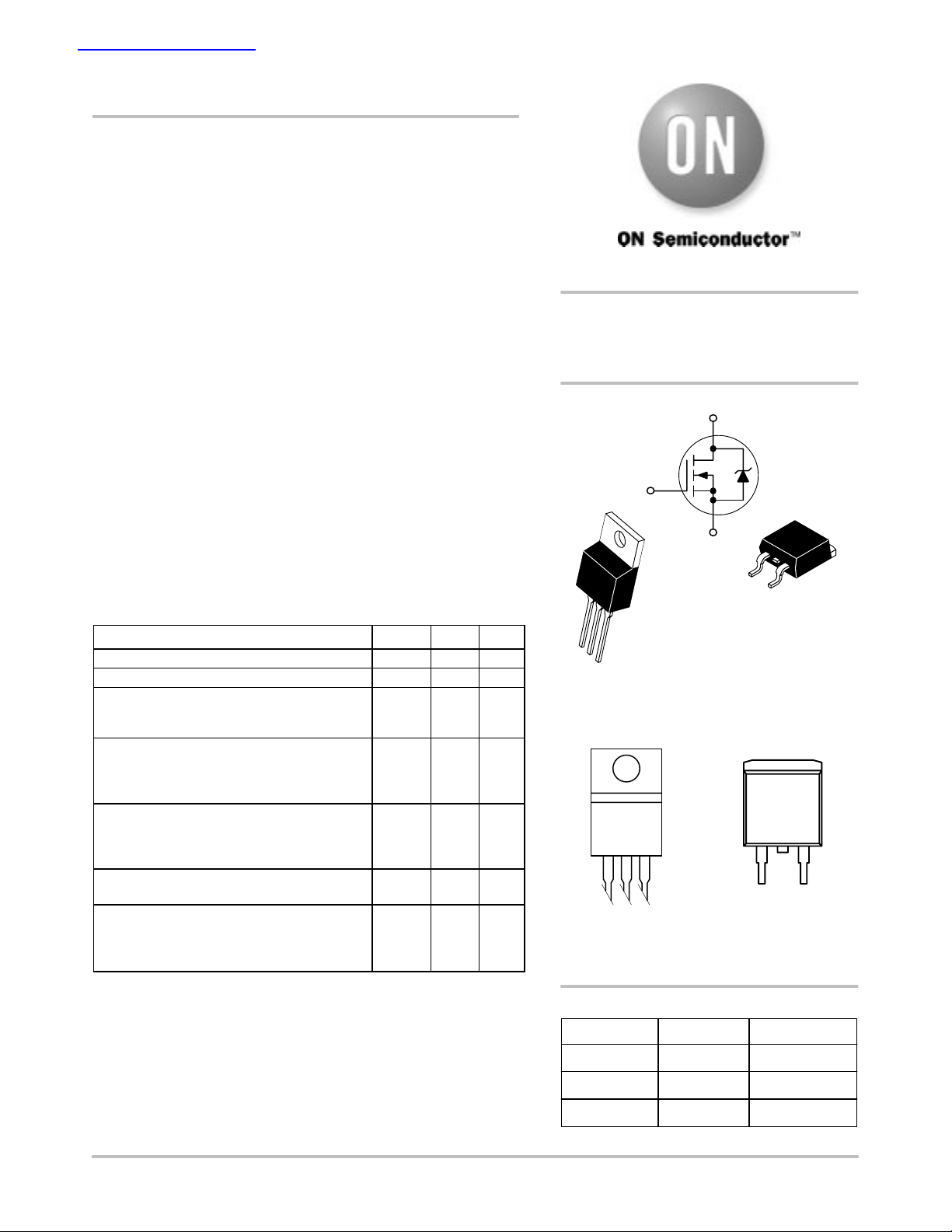
http://onsemi.com
45 AMPERES
60 VOLTS
R
DS(on)
G
4
TO–220AB
CASE 221A
1
2
3
STYLE 5
MARKING DIAGRAMS
& PIN ASSIGNMENTS
4
Drain
NTP45N06
LLYWW
1
Gate
3
Source
2
Drain
ORDERING INFORMATION
Device Package Shipping
= 26 mΩ
N–Channel
D
S
1
2
3
D2PAK
CASE 418B
STYLE 2
4
Drain
NTB45N06
LLYWW
1
Gate
NTx45N06 = Device Code
LL = Location Code
Y = Year
WW = Work Week
2
Drain
4
3
Source
Semiconductor Components Industries, LLC, 2001
March, 2001 – Rev . 0
NTP45N06 TO–220AB 50 Units/Rail
NTB45N06 D2PAK 50 Units/Rail
NTB45N06T4 D2PAK 800/Tape & Reel
1 Publication Order Number:
NTP45N06/D
Page 2
NTP45N06, NTB45N06
)
f = 1.0 MHz)
(V
DD
Vdc, I
D
Adc
)
V
GS
Vdc) (Note 5.)
)
dIS/dt = 100 A/µs) (Note 5.)
MAXIMUM RATINGS (T
Thermal Resistance – Junction–to–Case
Maximum Lead Temperature for Soldering Purposes, 1/8″ from case for 10 seconds T
ELECTRICAL CHARACTERISTICS (T
OFF CHARACTERISTICS
Drain–to–Source Breakdown Voltage (Note 5.)
(VGS = 0 Vdc, ID = 250 µAdc)
Temperature Coefficient (Positive)
Zero Gate Voltage Drain Current
(VDS = 60 Vdc, VGS = 0 Vdc)
(VDS = 60 Vdc, VGS = 0 Vdc, TJ = 150°C)
Gate–Body Leakage Current (VGS = ±20 Vdc, VDS = 0 Vdc) I
ON CHARACTERISTICS (Note 5.)
Gate Threshold Voltage (Note 5.)
(VDS = VGS, ID = 250 µAdc)
Threshold Temperature Coefficient (Negative)
Static Drain–to–Source On–Resistance (Note 5.)
(VGS = 10 Vdc, ID = 22.5 Adc)
Static Drain–to–Source On–Voltage (Note 5.)
(VGS = 10 Vdc, ID = 45 Adc)
(VGS = 10 Vdc, ID = 22.5 Adc, TJ = 150°C)
Forward Transconductance (Note 5.) (VDS = 8.0 Vdc, ID = 12 Adc) g
DYNAMIC CHARACTERISTICS
Input Capacitance
Output Capacitance
Transfer Capacitance
SWITCHING CHARACTERISTICS (Note 6.)
Turn–On Delay Time
Rise Time
Turn–Off Delay Time
Fall Time t
Gate Charge
SOURCE–DRAIN DIODE CHARACTERISTICS
Forward On–Voltage
Reverse Recovery Time
Reverse Recovery Stored Charge Q
3. When surface mounted to an FR4 board using 1″ pad size, (Cu Area 1.127 in2).
4. When surface mounted to an FR4 board using the minimum recommended pad size, (Cu Area 0.412 in2).
5. Pulse Test: Pulse Width ≤300 µs, Duty Cycle ≤ 2%.
6. Switching characteristics are independent of operating junction temperatures.
= 25°C unless otherwise noted)
J
Rating
– Junction–to–Ambient (Note 3.)
– Junction–to–Ambient (Note 4.)
= 25°C unless otherwise noted)
J
Characteristic
(VDS = 25 Vdc, VGS = 0 Vdc,
VGS = 10 Vdc, RG = 9.1 Ω) (Note 5.)
(IS = 45 Adc, VGS = 0 Vdc) (Note 5.)
(IS = 45 Adc, VGS = 0 Vdc, TJ = 150°C)
f = 1.0 MHz
(VDD = 30 Vdc, ID = 45 Adc,
30
(VDS = 48 Vdc, ID = 45 Adc,
= 10 Vdc) (Note 5.
= 10
V
(IS = 45 Adc, VGS = 0 Vdc,
dI
/dt = 100 A/µs) (Note 5.
45
Symbol Value Unit
R
θJC
R
θJA
R
θJA
L
Symbol Min Typ Max Unit
V
(BR)DSS
I
DSS
GSS
V
GS(th)
R
DS(on)
V
DS(on)
FS
C
iss
C
oss
C
rss
t
d(on)
t
t
d(off)
Q
Q
Q
V
SD
t
t
t
RR
r
f
T
1
2
rr
a
b
,
60
–
–
–
– – ±100 nAdc
2.0
–
– 21 26
–
–
– 16.6 – mhos
– 1224 1725 pF
– 345 485
– 76 160
– 10 25 ns
– 101 200
– 33 70
– 106 220
– 33 46 nC
– 6.4 –
– 15 –
–
–
– 53.1 –
– 36 –
– 16.9 –
– 0.087 – µC
1.2
46.8
63.2
260 °C
70
57
–
–
2.8
7.2
0.93
0.93
1.08
0.93
1.0
10
4.0
1.4
1.2
°C/W
–
–
–
–
–
Vdc
mV/°C
µAdc
Vdc
mV/°C
mOhm
Vdc
Vdc
ns
http://onsemi.com
2
Page 3
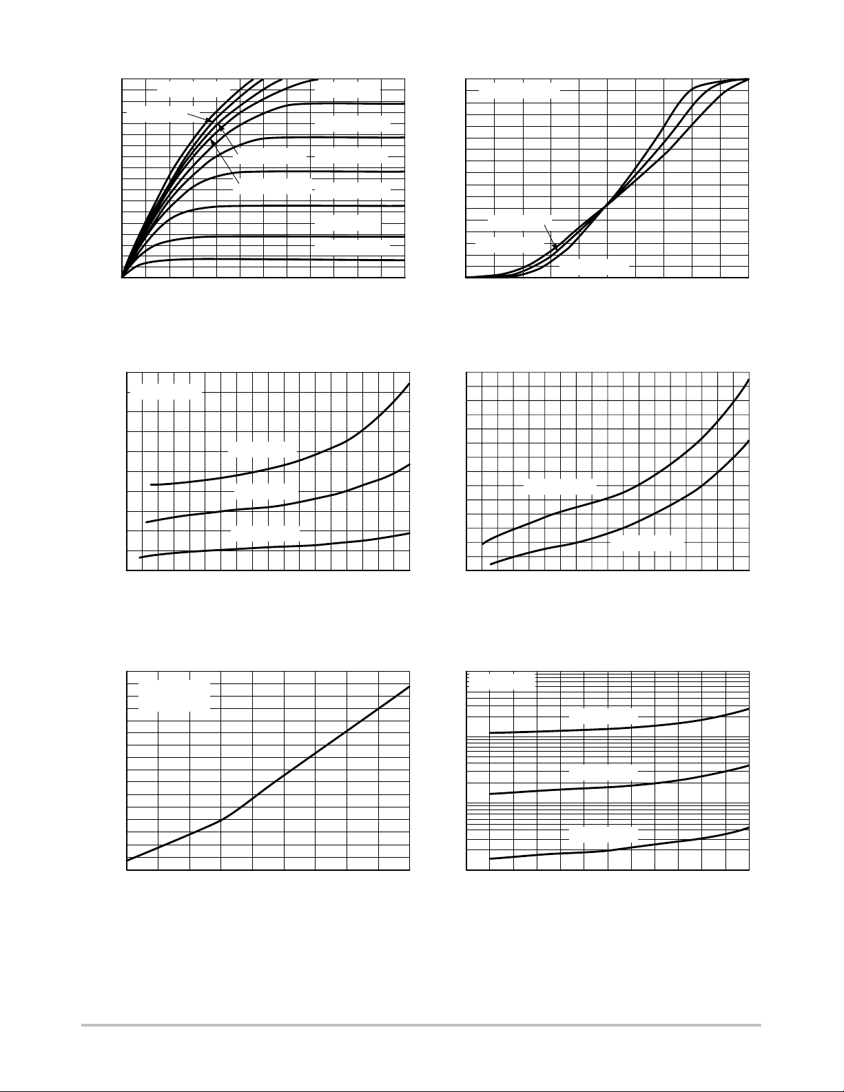
NTP45N06, NTB45N06
90
80
70
60
50
40
30
, DRAIN CURRENT (AMPS)
20
D
I
10
0
0
VGS = 10 V
VGS = 9 V
21
VDS, DRAIN–TO–SOURCE VOLTAGE (VOLTS)
Figure 1. On–Region Characteristics Figure 2. Transfer Characteristics
0.05
VGS = 10 V
0.042
0.034
VGS = 8 V
VGS = 7.5 V
3
TJ = 100°C
VGS = 7 V
VGS = 6.5 V
VGS = 6 V
VGS = 5.5 V
VGS = 5 V
VGS = 4.5 V
4 5 5.5 6 6.5 7 7.5
6
90
VDS > = 10 V
80
70
60
50
40
30
, DRAIN CURRENT (AMPS)
20
D
I
10
0.032
0.03
0.028
0.026
TJ = 25°C
TJ = 100°C
0
35 84.543.5
VGS, GATE–TO–SOURCE VOLTAGE (VOLTS)
TJ = –55°C
0.026
0.018
, DRAIN–TO–SOURCE RESISTANCE (Ω)
0.01
DS(on)
R
0
10 50 60 90
ID, DRAIN CURRENT (AMPS) ID, DRAIN CURRENT (AMPS)
TJ = 25°C
TJ = –55°C
403020
Figure 3. On–Resistance vs. Gate–to–Source
Voltage
2.2
ID = 22.5 A
2
VGS = 10 V
1.8
1.6
1.4
1.2
(NORMALIZED)
1
, DRAIN–TO–SOURCE RESISTANCE
0.8
0.6
DS(on)
–50 50250–25 75 125100
R
TJ, JUNCTION TEMPERATURE (°C) VDS, DRAIN–TO–SOURCE VOLTAGE (VOLTS)
0.024
0.022
0.02
, DRAIN–TO–SOURCE RESISTANCE (Ω)
70 0 40302010 50 60 9070
80 80
0.018
DS(on)
R
VGS = 10 V
VGS = 15 V
Figure 4. On–Resistance vs. Drain Current and
Gate Voltage
10000
, LEAKAGE (nA)
I
175150
VGS = 0 V
TJ = 150°C
1000
TJ = 125°C
DSS
100
TJ = 100°C
10
030402010 50 60
Figure 5. On–Resistance Variation with
Temperature
http://onsemi.com
Figure 6. Drain–to–Source Leakage Current
vs. Voltage
3
Page 4

NTP45N06, NTB45N06
3600
3200
2800
2400
2000
1600
1200
C, CAPACITANCE (pF)
VDS = 0 V
C
iss
C
rss
800
400
0
10
GATE–TO–SOURCE OR DRAIN–TO–SOURCE VOLTAGE
V
5
VGS = 0 V
GSVDS
(VOLTS)
C
iss
C
oss
C
rss
10
155020
Figure 7. Capacitance Variation Figure 8. Gate–to–Source and
1000
VDS = 30 V
ID = 45 A
VGS = 10 V
t
100
f
t
r
t
d(off)
TJ = 25°C
12
10
8
Q
6
4
2
, GATE–TO–SOURCE VOLTAGE (VOLTS)
0
GS
V
25 0 16 20128244
Drain–to–Source Voltage vs. Total Charge
50
VGS = 0 V
TJ = 25°C
40
30
Q
T
V
GS
Q
1
Qg, TOTAL GATE CHARGE (nC)
2
ID = 45
TJ = 25°C
28 32 36
t, TIME (ns)
10
1
1 10 100 0.6 0.76 0.80.720.68 0.920.64 1.04
t
d(on)
RG, GATE RESISTANCE (Ω)V
Figure 9. Resistive Switching Time Variation
20
10
, SOURCE CURRENT (AMPS)
S
I
0
, SOURCE–TO–DRAIN VOLTAGE (VOLTS)
SD
0.84 0.88 0.96
Figure 10. Diode Forward Voltage vs. Current
vs. Gate Resistance
1000
VGS = 20 V
SINGLE PULSE
TC = 25°C
100
dc
DS(on)
10 ms
Limit
1 ms
100 µs
10
1
, DRAIN CURRENT (AMPS)
D
I
0.1
0.10 10 1001 25 125 15010075 17550
R
Thermal Limit
Package Limit
VDS, DRAIN–TO–SOURCE VOLTAGE (VOLTS) TJ, STARTING JUNCTION TEMPERATURE (°C)
Figure 11. Maximum Rated Forward Biased
Safe Operating Area
280
240
200
160
120
AVALANCHE ENERGY (mJ)
, SINGLE PULSE DRAIN–TO–SOURCE
AS
E
ID = 45 A
80
40
0
Figure 12. Maximum Avalanche Energy vs.
Starting Junction Temperature
1
http://onsemi.com
4
Page 5

NTP45N06, NTB45N06
1
Normalized to R
0.1
EFFECTIVE TRANSIENT THERMAL RESPONSE (NORMALIZED)
r(t),
at Steady State
θJC
0.01
0.00001 10.10.010.0010.0001 10
t, TIME (s)
Figure 13. Thermal Response
10
Normalized to R
1″ square Cu Pad, Cu Area 1.127 in2,
3 x 3 inch FR4 board
1
0.1
0.01
at Steady State,
θJA
r(t), EFFECTIVE TRANSIENT THERMAL RESISTANCE (NORMALIZED)
0.001
0.00001 0.001 0.01
10001001010.10.0001
t, TIME (s)
Figure 14. Thermal Response
http://onsemi.com
5
Page 6

NTP45N06, NTB45N06
PACKAGE DIMENSIONS
TO–220 THREE–LEAD
TO–220AB
CASE 221A–09
ISSUE AA
SEATING
–T–
PLANE
B
4
Q
123
F
T
A
U
C
S
H
K
Z
L
V
R
J
G
D
N
NOTES:
1. DIMENSIONING AND TOLERANCING PER ANSI
Y14.5M, 1982.
2. CONTROLLING DIMENSION: INCH.
3. DIMENSION Z DEFINES A ZONE WHERE ALL
BODY AND LEAD IRREGULARITIES ARE
ALLOWED.
DIM MIN MAX MIN MAX
A 0.570 0.620 14.48 15.75
B 0.380 0.405 9.66 10.28
C 0.160 0.190 4.07 4.82
D 0.025 0.035 0.64 0.88
F 0.142 0.147 3.61 3.73
G 0.095 0.105 2.42 2.66
H 0.110 0.155 2.80 3.93
J 0.018 0.025 0.46 0.64
K 0.500 0.562 12.70 14.27
L 0.045 0.060 1.15 1.52
N 0.190 0.210 4.83 5.33
Q 0.100 0.120 2.54 3.04
R 0.080 0.110 2.04 2.79
S 0.045 0.055 1.15 1.39
T 0.235 0.255 5.97 6.47
U 0.000 0.050 0.00 1.27
V 0.045 --- 1.15 ---
Z --- 0.080 --- 2.04
STYLE 5:
PIN 1. GATE
2. DRAIN
3. SOURCE
4. DRAIN
MILLIMETERSINCHES
http://onsemi.com
6
Page 7

–T–
SEATING
PLANE
–B–
G
NTP45N06, NTB45N06
PACKAGE DIMENSIONS
D2PAK
CASE 418B–03
ISSUE D
C
E
V
4
A
231
S
K
J
3 PL
D
0.13 (0.005) T
M
M
B
H
NOTES:
1. DIMENSIONING AND TOLERANCING PER ANSI
Y14.5M, 1982.
2. CONTROLLING DIMENSION: INCH.
DIM MIN MAX MIN MAX
A 0.340 0.380 8.64 9.65
B 0.380 0.405 9.65 10.29
C 0.160 0.190 4.06 4.83
D 0.020 0.035 0.51 0.89
E 0.045 0.055 1.14 1.40
G 0.100 BSC 2.54 BSC
H 0.080 0.110 2.03 2.79
J 0.018 0.025 0.46 0.64
K 0.090 0.110 2.29 2.79
S 0.575 0.625 14.60 15.88
V 0.045 0.055 1.14 1.40
STYLE 2:
PIN 1. GATE
2. DRAIN
3. SOURCE
4. DRAIN
MILLIMETERSINCHES
http://onsemi.com
7
Page 8

NTP45N06, NTB45N06
ON Semiconductor and are trademarks of Semiconductor Components Industries, LLC (SCILLC). SCILLC reserves the right to make changes
without further notice to any products herein. SCILLC makes no warranty, representation or guarantee regarding the suitability of its products for any particular
purpose, nor does SCILLC assume any liability arising out of the application or use of any product or circuit, and specifically disclaims any and all liability,
including without limitation special, consequential or incidental damages. “Typical” parameters which may be provided in SCILLC data sheets and/or
specifications can and do vary in different applications and actual performance may vary over time. All operating parameters, including “Typicals” must be
validated for each customer application by customer’s technical experts. SCILLC does not convey any license under its patent rights nor the rights of others.
SCILLC products are not designed, intended, or authorized for use as components in systems intended for surgical implant into the body, or other applications
intended to support or sustain life, or for any other application in which the failure of the SCILLC product could create a situation where personal injury or
death may occur. Should Buyer purchase or use SCILLC products for any such unintended or unauthorized application, Buyer shall indemnify and hold
SCILLC and its officers, employees, subsidiaries, affiliates, and distributors harmless against all claims, costs, damages, and expenses, and reasonable
attorney fees arising out of, directly or indirectly, any claim of personal injury or death associated with such unintended or unauthorized use, even if such claim
alleges that SCILLC was negligent regarding the design or manufacture of the part. SCILLC is an Equal Opportunity/Affirmative Action Employer.
PUBLICATION ORDERING INFORMATION
NORTH AMERICA Literature Fulfillment:
Literature Distribution Center for ON Semiconductor
P.O. Box 5163, Denver, Colorado 80217 USA
Phone: 303–675–2175 or 800–344–3860 Toll Free USA/Canada
Fax: 303–675–2176 or 800–344–3867 Toll Free USA/Canada
Email: ONlit@hibbertco.com
Fax Response Line: 303–675–2167 or 800–344–3810 Toll Free USA/Canada
N. American Technical Support: 800–282–9855 Toll Free USA/Canada
EUROPE: LDC for ON Semiconductor – European Support
German Phone: (+1) 303–308–7140 (Mon–Fri 2:30pm to 7:00pm CET)
Email: ONlit–german@hibbertco.com
French Phone: (+1) 303–308–7141 (Mon–Fri 2:00pm to 7:00pm CET)
Email: ONlit–french@hibbertco.com
English Phone: (+1) 303–308–7142 (Mon–Fri 12:00pm to 5:00pm GMT)
Email: ONlit@hibbertco.com
EUROPEAN TOLL–FREE ACCESS*: 00–800–4422–3781
*Available from Germany, France, Italy, UK, Ireland
CENTRAL/SOUTH AMERICA:
Spanish Phone: 303–308–7143 (Mon–Fri 8:00am to 5:00pm MST)
Email: ONlit–spanish@hibbertco.com
Toll–Free from Mexico: Dial 01–800–288–2872 for Access –
then Dial 866–297–9322
ASIA/PACIFIC: LDC for ON Semiconductor – Asia Support
Phone: 303–675–2121 (Tue–Fri 9:00am to 1:00pm, Hong Kong Time)
Toll Free from Hong Kong & Singapore:
001–800–4422–3781
Email: ONlit–asia@hibbertco.com
JAPAN: ON Semiconductor, Japan Customer Focus Center
4–32–1 Nishi–Gotanda, Shinagawa–ku, Tokyo, Japan 141–0031
Phone: 81–3–5740–2700
Email: r14525@onsemi.com
ON Semiconductor Website: http://onsemi.com
For additional information, please contact your local
Sales Representative.
http://onsemi.com
8
NTP45N06/D
 Loading...