

ON Semiconductor NTMFS0D8N02P1E User Manual
MOSFET - Power, Single
N-Channel, SO8-FL
25 V, 0.68 mW, 365 A
NTMFS0D8N02P1E
Features
• Small Footprint (5x6mm) for Compact Design
• Low R
• Low Q
• These Devices are Pb−Free, Halogen Free/BFR Free and are RoHS
Compliant
Applications
• DC−DC Converters
• Power Load Switch
• Notebook Battery Management
to Minimize Conduction Losses
DS(on)
and Capacitance to Minimize Driver Losses
G
V
(BR)DSS
25 V
www.onsemi.com
R
MAX ID MAX
DS(ON)
0.68 mW @ 10 V
0.80 mW @ 4.5 V
D (5−8)
365 A
MAXIMUM RATINGS (T
Parameter
Drain−to−Source Voltage V
Gate−to−Source Voltage V
Continuous Drain
Current R
(Note 1)
Power Dissipation
R
Continuous Drain
Current R
(Notes 1, 3)
Power Dissipation
R
Continuous Drain
Current R
(Notes 2, 3)
Power Dissipation
R
Pulsed Drain Current
Single Pulse Drain−to−Source Avalanche
Energy (I
Operating Junction and Storage Temperature
Range
Lead Temperature for Soldering Purposes
(1/8″ from case for 10 s)
Stresses exceeding those listed in the Maximum Ratings table may damage the
device. If any of these limits are exceeded, device functionality should not be
assumed, damage may occur and reliability may be affected.
1. Surface−mounted on FR4 board using 1 in
2. Surface−mounted on FR4 board using minimum pad size, 2 oz Cu pad.
3. The entire application environment impacts the thermal resistance values
4. 100% UIS tested at L = 1 mH, I
q
JC
(Note 1)
q
JC
q
JA
(Notes 1, 3)
q
JA
q
JA
(Notes 2, 3)
q
JA
= 115.4 Apk, L = 0.1 mH) (Note 4)
L
shown, they are not constants and are only valid for the particular conditions
noted. Actual continuous current will be limited by thermal & electro−mechanical
application board design. R
= 25°C unless otherwise stated)
J
Symbol Value Unit
DSS
GS
TC = 25°C
Steady
State
Steady
State
Steady
State
TA = 25°C, tp = 10 ms
TC =85°C 263
TC = 25°C P
TA = 25°C
TA = 85°C 40
TA = 25°C P
TA = 25°C
TA = 85°C 21
TA = 25°C P
is determined by the user’s board design.
q
JC
= 30.7 A.
AS
I
D
D
I
D
D
I
D
D
I
DM
E
AS
TJ, T
STG
T
L
2
pad size, 2 oz Cu pad.
25 V
+16/
−12
365
139 W
55
3.2 W
30
0.93 W
762 A
666 mJ
−55 to
+150
260 °C
V
A
A
A
°C
G (4)
S (1,2,3)
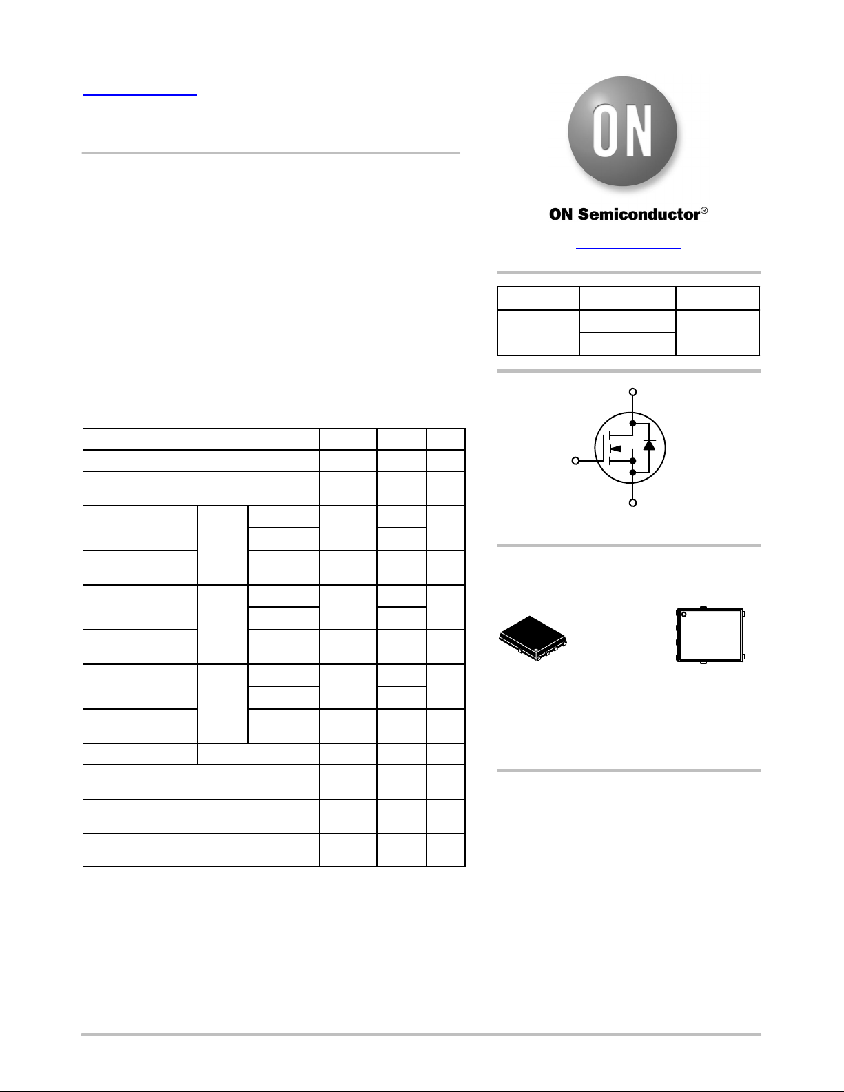
N−CHANNEL MOSFET
MARKING
DIAGRAMS
D
SO−8 FLAT LEAD
CASE 488AA
STYLE 1
1
2EFN = Specific Device Code
A = Assembly Location
Y = Year
W = Work Week
ZZ = Lot Traceabililty
S
S
S
G
2EFN
AYWZZ
D
ORDERING INFORMATION
See detailed ordering, marking and shipping information in the
package dimensions section on page 6 of this data sheet.
D
D
© Semiconductor Components Industries, LLC, 2019
April, 2021 − Rev. 1
1 Publication Order Number:
NTMFS0D8N02P1E/D
THERMAL RESISTANCE MAXIMUM RATINGS
Parameter Symbol Value Unit
Junction−to−Case – Steady State (Note 1)
Junction−to−Ambient – Steady State (Note 1)
Junction−to−Ambient – Steady State (Note 2)
NTMFS0D8N02P1E
R
q
JC
R
q
JA
R
q
JA
0.9
39
°C/W
135 °C/W
ELECTRICAL CHARACTERISTICS (T
Parameter
= 25°C unless otherwise specified)
J
Symbol Test Condition Min Typ Max Unit
OFF CHARACTERISTICS
Drain−to−Source Breakdown Voltage
Drain−to−Source Breakdown Voltage
Temperature Coefficient
Zero Gate Voltage Drain Current I
Gate−to−Source Leakage Current I
V
(BR)DSS
V
(BR)DSS
DSS
GSS
T
J
ON CHARACTERISTICS (Note 5)
Gate Threshold Voltage
Threshold Temperature Coefficient V
Drain−to−Source On Resistance R
Forward Transconductance g
Gate Resistance R
V
GS(TH)
GS(TH)/TJ
DS(on)
FS
G
CHARGES AND CAPACITANCES
Input Capacitance
Output Capacitance C
Reverse Transfer Capacitance C
Total Gate Charge Q
Threshold Gate Charge Q
Gate−to−Source Charge Q
Gate−to−Drain Charge Q
Total Gate Charge Q
C
ISS
OSS
RSS
G(TOT)
G(TH)
GS
GD
G(TOT)
SWITCHING CHARACTERISTICS, VGS = 4.5 V (Note 6)
Turn−On Delay Time
Rise Time t
Turn−Off Delay Time t
Fall Time t
t
d(ON)
r
d(OFF)
f
SWITCHING CHARACTERISTICS, VGS = 10 V (Note 6)
Turn−On Delay Time
Rise Time t
Turn−Off Delay Time t
Fall Time t
t
d(ON)
r
d(OFF)
f
DRAIN−SOURCE DIODE CHARACTERISTICS
Forward Diode Voltage V
SD
VGS = 0 V, ID = 1 mA 25 V
/
ID = 1 mA. ref to 25°C 16
VGS = 0 V,
V
= 20 V
DS
TJ = 25°C 1
TJ = 125°C 250
VDS = 0 V, VGS = +16 V/−12 V ±100 nA
VGS = VDS, ID = 2 mA 1.2 2.0 V
ID = 2 mA. ref to 25°C −4.4 mV/°C
VGS = 10 V, ID = 46 A 0.44 0.68
VGS = 4.5 V, ID = 43 A 0.54 0.80
VDS = 5 V, ID = 46 A 307 S
TA = 25°C 0.48
8600
VGS = 0 V, VDS = 13 V, f = 1 MHz
2285
129
52
10
VGS = 4.5 V, VDS = 13 V; ID = 46 A
21
9
VGS = 10 V, VDS = 13 V; ID = 46 A 116 nC
45
VGS = 4.5 V, VDS = 13 V,
= 46 A, RG = 6.0 W
I
D
24
68
20
23
VGS = 10 V, VDS = 13 V,
= 46 A, RG = 6.0 W
I
D
6.8
123
19
VGS = 0 V,
I
= 46 A
S
TJ = 25°C 0.77 1.2
TJ = 125°C 0.62
mV/°C
mA
mW
W
pF
nC
ns
ns
V
www.onsemi.com
2

NTMFS0D8N02P1E
ELECTRICAL CHARACTERISTICS (T
Parameter UnitMaxTypMinTest ConditionSymbol
DRAIN−SOURCE DIODE CHARACTERISTICS
Reverse Recovery Time
Reverse Recovery Charge Q
Product parametric performance is indicated in the Electrical Characteristics for the listed test conditions, unless otherwise noted. Product
performance may not be indicated by the Electrical Characteristics if operated under different conditions.
5. Pulse Test: pulse width v 300 ms, duty cycle v 2%.
6. Switching characteristics are independent of operating junction temperatures.
= 25°C unless otherwise specified)
J
t
RR
RR
VGS = 0 V, dIS/dt = 100 A/ms,
IS = 46 A
64 ns
87 nC
www.onsemi.com
3
 Loading...