

ON Semiconductor NTMFS0D7N03CG User Manual
MOSFET - Power, Single
N-Channel, SO8-FL
30 V, 0.65 mW, 409 A
NTMFS0D7N03CG
Features
• Wide SOA to Improve Inrush Current Management
• Advanced Package (5x6mm) with Excellent Thermal Conduction
• Ultra Low R
• These Devices are Pb−Free, Halogen Free/BFR Free and are RoHS
Compliant
Applications
• Hot Swap Application
• Power Load Switch
• Battery Management and Protection
to Improve System Efficiency
DS(on)
V
(BR)DSS
30 V
www.onsemi.com
R
MAX ID MAX
DS(ON)
0.65 mW @ 10 V
D (5−8)
409 A
MAXIMUM RATINGS (T
Parameter
Drain−to−Source Voltage V
Gate−to−Source Voltage V
Continuous Drain
Current R
(Note 2)
Power Dissipation
R
Continuous Drain
Current R
(Notes 1, 2)
Power Dissipation
R
Pulsed Drain Current
Source Current (Body Diode) I
Single Pulse Drain−to−Source Avalanche
Energy (I
Operating Junction and Storage Temperature
Range
Lead Temperature for Soldering Purposes
(1/8″ from case for 10 s)
Stresses exceeding those listed in the Maximum Ratings table may damage the
device. If any of these limits are exceeded, device functionality should not be
assumed, damage may occur and reliability may be affected.
1. Surface−mounted on FR4 board using 1 in
2. The entire application environment impacts the thermal resistance values shown,
q
JC
(Note 2)
q
JC
q
JA
(Notes 1, 2)
q
JA
= 40.8 Apk)
L
they are not constants and are only valid for the particular conditions noted.
= 25°C unless otherwise stated)
J
Symbol Value Unit
TC = 25°C
Steady
State
Steady
State
TA = 25°C, tp = 10 ms
TC =100°C 289
TC = 25°C P
TA = 25°C
TA = 100°C 42
TA = 25°C P
TJ, T
2
pad, 2 oz Cu pad.
I
E
DSS
GS
I
D
D
I
D
D
DM
S
AS
T
L
STG
30 V
±20 V
409
187 W
59
4.0 W
900 A
155 A
1080 mJ
−55 to
+175
260 °C
A
A
°C
G (4)
S (1,2,3)
N−CHANNEL MOSFET
MARKING
DIAGRAMS
D
G
S
S
S
0D7NG
AYWZZ
D
SO−8 FLAT LEAD
CASE 488AA
STYLE 1
1
A = Assembly Location
Y = Year
W = Work Week
ZZ = Lot Traceabililty
ORDERING INFORMATION
See detailed ordering, marking and shipping information in the
package dimensions section on page 5 of this data sheet.
D
D
© Semiconductor Components Industries, LLC, 2019
April, 2021 − Rev. 4
1 Publication Order Number:
NTMFS0D7N03CG/D
THERMAL RESISTANCE MAXIMUM RATINGS
Parameter Symbol Value Unit
Junction−to−Case – Steady State (Note 1)
Junction−to−Ambient – Steady State (Note 1)
Junction−to−Ambient – Steady State (Note 2)
NTMFS0D7N03CG
R
q
JC
R
q
JA
R
q
JA
0.8
38
°C/W
134 °C/W
ELECTRICAL CHARACTERISTICS (T
Parameter
= 25°C unless otherwise specified)
J
Symbol Test Condition Min Typ Max Unit
OFF CHARACTERISTICS
Drain−to−Source Breakdown Voltage
Drain−to−Source Breakdown Voltage
V
V
Temperature Coefficient
Zero Gate Voltage Drain Current I
Gate−to−Source Leakage Current I
(BR)DSS
(BR)DSS
T
J
DSS
GSS
VGS = 0 V, ID = 250 mA
/
ID = 250 mA. ref to 25°C
VGS = 0 V,
V
= 30 V
DS
TJ = 125°C 100
TJ = 25°C 1.0
VDS = 0 V, VGS = 20 V 100 nA
30 V
11
mV/°C
mA
ON CHARACTERISTICS (Note 3)
Gate Threshold Voltage
Threshold Temperature Coefficient V
V
GS(TH)/TJ
Drain−to−Source On Resistance R
Forward Transconductance g
Gate Resistance R
GS(TH)
DS(on)
FS
G
VGS = VDS, ID = 280 mA
ID = 280 mA. ref to 25°C
VGS = 10 V, ID = 30 A 0.55 0.65
VDS = 3 V, ID = 30 A 100 S
TA = 25°C 0.4
1.3 2.2 V
−5.1 mV/°C
mW
W
CHARGES AND CAPACITANCES
Input Capacitance
Output Capacitance C
Reverse Transfer Capacitance C
Total Gate Charge Q
Threshold Gate Charge Q
Gate−to−Source Charge Q
Gate−to−Drain Charge Q
C
ISS
OSS
RSS
G(TOT)
G(TH)
GS
GD
VGS = 0 V, VDS = 15 V, f = 1 MHz
VGS = 10 V, VDS = 15 V; ID = 30 A
12300
5800
88
147
19
34
8.6
pF
nC
SWITCHING CHARACTERISTICS (Note 4)
Turn−On Delay Time
t
Rise Time t
Turn−Off Delay Time t
d(OFF)
Fall Time t
d(ON)
r
f
VGS = 10 V, VDS = 15 V,
= 30 A, RG = 3.0 W
I
D
28
13
85
16
ns
DRAIN−SOURCE DIODE CHARACTERISTICS
Forward Diode Voltage
Reverse Recovery Time t
Reverse Recovery Charge Q
V
SD
RR
RR
VGS = 0 V,
I
= 30 A
S
VGS = 0 V, dIS/dt = 100 A/ms,
V
= 15 V, IS = 30 A
DS
TJ = 25°C 0.78 1.2
TJ = 125°C 0.62
98 ns
143 nC
V
Product parametric performance is indicated in the Electrical Characteristics for the listed test conditions, unless otherwise noted. Product
performance may not be indicated by the Electrical Characteristics if operated under different conditions.
3. Pulse Test: pulse width v 300 ms, duty cycle v 2%.
4. Switching characteristics are independent of operating junction temperatures.
www.onsemi.com
2
NTMFS0D7N03CG
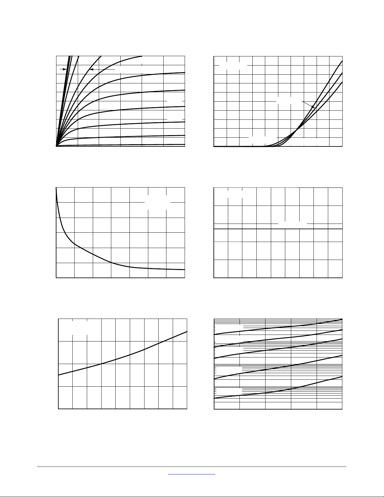
TYPICAL CHARACTERISTICS
500
450
400
350
300
250
200
150
, DRAIN CURRENT (A)
D
I
100
50
0
VDS, DRAIN−TO−SOURCE VOLTAGE (V) VGS, GATE−TO−SOURCE VOLTAGE (V)
Figure 1. On−Region Characteristics Figure 2. Transfer Characteristics
6
5
4
3
2
5.5 V
VGS = 10 V to 6 V
TJ = 25°C
I
D
= 30 A
5.0 V
4.5 V
4.0 V
3.5 V
3.0 V
2.5 V
500
450
400
350
300
250
200
150
, DRAIN CURRENT (A)
D
I
100
50
3.02.52.01.51.00.50
0
1.0
0.8
0.6
0.4
VDS = 3 V
1.51.0
TJ = 25°C
TJ = 25°C
TJ = 125°C
1.5 3.5
TJ = −55°C
2.5 4.0
3.02.00 4.5 5.0
VGS = 10 V
, DRAIN−TO−SOURCE RESISTANCE (mW)
DS(on)
R
, NORMALIZED DRAIN−TO−
SOURCE RESISTANCE
DS(on)
R
1
0
4
3
VGS, GATE VOLTAGE (V) ID, DRAIN CURRENT (A)
8765 40
Figure 3. On−Resistance vs. Gate−to−Source
Voltage
2.0
VGS = 10 V
= 30 A
I
D
1.5
1.0
0.5
0
TJ, JUNCTION TEMPERATURE (°C) VDS, DRAIN−TO−SOURCE VOLTAGE (V)
50
Figure 5. On−Resistance Variation with
Temperature
150
, DRAIN−TO−SOURCE RESISTANCE (mW)
109
DS(on)
R
1.E+05
1.E+04
1.E+03
, LEAKAGE (nA)
DSS
1.E+02
I
1.E+01
17512510075250−25−50
0.2
0
10 20 35 45
30 5025155
Figure 4. On−Resistance vs. Drain Current and
Gate Voltage
TJ = 175°C
TJ = 150°C
TJ = 125°C
TJ = 85°C
TJ = 25°C
15
Figure 6. Drain−to−Source Leakage Current
vs. Voltage
302520105
www.onsemi.com
3
 Loading...