

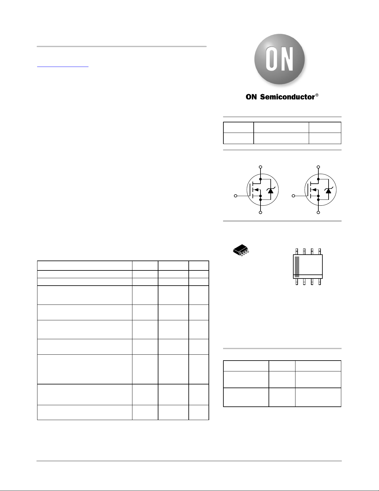
NTMD6N04, NVMD6N04
MOSFET – Power, Dual
N-Channel, SOIC-8
40 V, 5.8 A
Features
• Designed for use in low voltage, high speed switching applications
• Ultra Low On−Resistance Provides
Higher Efficiency and Extends Battery Life
− R
− R
• Miniature SOIC−8 Surface Mount Package Saves Board Space
• Diode is Characterized for Use in Bridge Circuits
• Diode Exhibits High Speed, with Soft Recovery
• NVMD Prefix for Automotive and Other Applications Requiring
Unique Site and Control Change Requirements; AEC−Q101
Qualified and PPAP Capable*
• These Devices are Pb−Free and are RoHS Compliant
Applications
• DC−DC Converters
• Computers
• Printers
• Cellular and Cordless Phones
• Disk Drives and Tape Drives
MAXIMUM RATINGS (T
Drain−to−Source Voltage V
Gate−to−Source Voltage − Continuous V
Drain Current (Note 1)
− Continuous @ T
− Single Pulse (tp ≤ 10 ms)
Drain Current (Note 2)
− Continuous @ T
Total Power Dissipation
@ T
= 25°C (Note 1)
A
@ TA = 25°C (Note 2)
Operating and Storage Temperature
Range
Single Pulse Drain−to−Source Avalanche
Energy − Starting T
(VDD = 40 Vdc, VGS = 5.0 Vdc,
Vdc, Peak IL = 7.0 Apk,
L = 10 mH, R
Thermal Resistance
− Junction−to−Ambient (Note 1)
− Junction−to−Ambient (Note 2)
Maximum Lead Temperature for
Soldering Purposes for 10 Sec
Stresses exceeding Maximum Ratings may damage the device. Maximum
Ratings are stress ratings only. Functional operation above the Recommended
Operating Conditions is not implied. Extended exposure to stresses above the
Recommended Operating Conditions may affect device reliability.
1. When surface mounted to an FR4 board using 1″ pad size, t ≤ 10 s
= 0.027 W, VGS = 10 V (Typ)
DS(on)
= 0.034 W, VGS = 4.5 V (Typ)
DS(on)
= 25°C unless otherwise noted)
J
Rating
= 25°C
A
= 25°C
A
= 25°C
J
= 25 W)
G
Symbol Value Unit
DSS
I
I
DM
I
P
TJ, T
E
R
T
GS
D
D
AS
q
D
stg
JA
L
40 V
"20 V
5.8
29
4.6 Adc
2.0
1.29
−55 to +150 °C
245 mJ
62.5
97
260 °C
Adc
Apk
W
°C/W
http://onsemi.com
G
V
DSS
40 V
R
27 mW @ V
N−Channel
D
S
Typ ID Max
DS(ON)
= 10 V
GS
G
5.8 A
D
S
MARKING DIAGRAM &
PIN ASSIGNMENT
8
1
SOIC−8
CASE 751
STYLE 11
E6N04 = Specific Device Code
A = Assembly Location
Y = Year
WW = Work Week
G = Pb−Free Package
(Note: Microdot may be in either location)
D1 D1 D2 D2
8
E6N04
AYWW G
G
1
S1 G1 S2 G2
ORDERING INFORMATION
Device Package Shipping
NTMD6N04R2G SOIC−8
(Pb−Free)
NVMD6N04R2G* SOIC−8
(Pb−Free)
†For information on tape and reel specifications,
including part orientation and tape sizes, please
refer to our Tape and Reel Packaging Specification
Brochure, BRD8011/D.
2500 / Tape &
2500 / Tape &
†
Reel
Reel
© Semiconductor Components Industries, LLC, 2013
July, 2019 − Rev. 2
1 Publication Order Number:
NTMD6N04R2/D

NTMD6N04, NVMD6N04
2. When surface mounted to an FR4 board using 1″ pad size, t = steady state
http://onsemi.com
2
NTMD6N04, NVMD6N04
ELECTRICAL CHARACTERISTICS (T
= 25°C unless otherwise noted)
C
Characteristic
OFF CHARACTERISTICS
Drain−to−Source Breakdown Voltage
= 0 Vdc, ID = 250 mA)
(V
GS
Temperature Coefficient (Positive)
V
Zero Gate Voltage Drain Current
(V
= 40 Vdc, VGS = 0 Vdc, TJ = 25°C)
DS
(VDS = 40 Vdc, VGS = 0 Vdc, TJ = 125°C)
Gate−Body Leakage Current
(V
= ±20 Vdc, VDS = 0 Vdc)
GS
ON CHARACTERISTICS (Note 3)
Gate Threshold Voltage
= VGS, ID = 250 mAdc)
(V
DS
Temperature Coefficient (Negative)
Static Drain−to−Source On−State Resistance
(V
= 10 Vdc, ID = 5.8 Adc)
GS
= 4.5 Vdc, ID = 3.9 Adc)
(V
GS
Forward Transconductance
(V
= 10 Vdc, ID = 5.8 Adc)
DS
DYNAMIC CHARACTERISTICS
Input Capacitance
Output Capacitance C
(VDS = 32 Vdc, VGS = 0 Vdc,
f = 1.0 MHz)
Reverse Transfer Capacitance C
SWITCHING CHARACTERISTICS (Notes 3 & 4)
Turn−On Delay Time
Rise Time t
Turn−Off Delay Time t
(VDD = 20 Vdc, ID = 5.8 A,
V
= 10 V,
GS
= 6 W)
R
G
Fall Time t
Turn−On Delay Time
Rise Time t
Turn−Off Delay Time t
(VDD = 20 Vdc, ID = 5.8 A,
V
= 4.5 V,
GS
= 6 W)
R
G
Fall Time t
Gate Charge
(VDS = 20 Vdc,
V
= 10 Vdc,
GS
ID = 5.8 A)
BODY−DRAIN DIODE RATINGS (Note 3)
Diode Forward On−Voltage (IS = 1.7 Adc, VGS = 0 V)
(I
= 1.7 Adc, VGS = 0 V, TJ = 150°C)
S
Reverse Recovery Time
(IS = 1.7 A, VGS = 0 V,
/dt = 100 A/ms)
dI
S
Reverse Recovery Stored Charge
= 1.7 A, dIS/dt = 100 A/ms, VGS = 0 V)
(I
S
3. Pulse Test: Pulse Width ≤ 300 ms, Duty Cycle ≤ 2%.
4. Switching characteristics are independent of operating junction temperature.
Symbol Min Typ Max Unit
Vdc
V
(BR)DSS
(BR)DSS/TJ
I
DSS
I
GSS
40
−
−
−
47
45
−
−
−
−
1.0
10
− − "100
mV/°C
mAdc
nAdc
Vdc
V
GS(th)
V
GS(th)/TJ
R
DS(on)
g
FS
C
iss
oss
rss
t
d(on)
d(off)
t
d(on)
d(off)
Q
Q
gs
Q
gd
V
SD
t
rr
t
a
t
b
Q
RR
r
f
r
f
T
1.0
−
−
−
1.9
4.7
0.027
0.034
3.0
−
0.034
0.043
mV/°C
Mhos
− 8.12 −
− 723 900
− 156 225
− 53 75
− 10 18
− 20 35
− 45 70
− 40 65
− 15 −
− 55 −
− 30 −
− 35 −
− 20 30
− 2.5 −
− 5.5 −
−
−
0.76
0.56
1.1
−
− 23 −
− 16 −
− 7 −
− 20 − nC
Vdc
W
pF
ns
ns
nC
ns
http://onsemi.com
3
 Loading...