

查询NTLJF4156N供应商
NTLJF4156N
Power MOSFET and
Schottky Diode
30 V, 4.0 A, N−Channel, with 1.0 A
Schottky Barrier Diode, SC−88FL
2x2 mm, mCool] Package
http://onsemi.com
Features
• Leadless SMD Package Featuring a MOSFET and Schottky Diode
• Better Thermal Resistance than TSOP−6 Package
• R
Rated at Low V
DS(on)
Levels, VGS = 1.5 V
GS(on)
• Low VF Schottky
• This is a Pb−Free Device
Applications
• DC−DC Converters
• Li−Ion Battery Applications in Cell Phones, PDA’s, Media Players
• Color Display and Camera Flash Regulators
MAXIMUM RATINGS (T
Parameter Symbol Value Unit
Drain−to−Source Voltage V
Gate−to−Source Voltage V
Continuous Drain
Current (Note 1)
Power Dissipation
(Note 1)
Continuous Drain
Current (Note 2)
Power Dissipation
(Note 2)
Pulsed Drain Current
Operating Junction and Storage Temperature TJ, T
Source Current (Body Diode) (Note 2) I
Lead Temperature for Soldering Purposes
(1/8″ from case for 10 s)
Maximum ratings are those values beyond which device damage can occur.
Maximum ratings applied to the device are individual stress limit values (not
normal operating conditions) and are not valid simultaneously . If these limits are
exceeded, device functional operation is not implied, damage may occur and
reliability may be affected.
1. Surface Mounted on FR4 Board using 1 in sq pad size (Cu area = 1.127 in sq
[1 oz] including traces).
2. Surface Mounted on FR4 Board using the minimum recommended pad size.
= 25°C unless otherwise noted)
J
DSS
GS
I
I
P
I
P
DM
T
D
D
D
D
STG
S
L
T
= 25°C
Steady
State
t ≤ 5 s T
Steady
State
t ≤ 5 s 2.08
Steady
State
J
T
= 85°C 2.4
J
= 25°C 4.0
J
T
= 25°C
J
T
= 25°C
J
T
= 85°C 1.4
J
T
= 25°C
J
t
= 10 ms
p
30 V
±8.0 V
3.0
1.21
2.0
0.44
17 A
−55 to
150
2.4 A
260 °C
A
W
A
°C
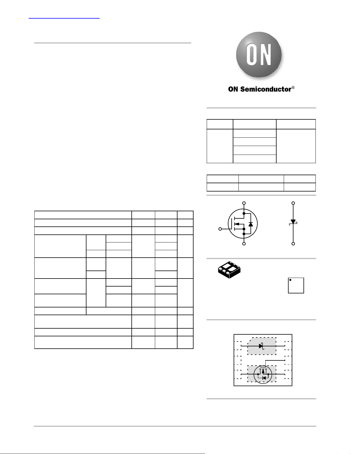
MOSFET
(BR)DSS
30 V
MAX
R
DS(on)
70 mW @ 4.5 V
90 mW @ 2.5 V
125 mW @ 1.8 V
250 mW @ 1.5 V
ID MAX (Note 1)V
SCHOTTKY DIODE
VR MAX IF MAXVF TYP
30 V
G
N−CHANNEL MOSFET
0.48 V
D
S
A
K
SCHOTTKY DIODE
MARKING
DIAGRAM
1
DFN6
CASE 506AN
JL = Specific Device Code
M = Date Code
G = Pb−Free Package
(Note: Microdot may be in either location)
1
2
3
PIN CONNECTIONS
K
6
5
D
4
N/C
A
1
2
D
3
(Top View)
4.0 A
1.0 A
JLMG
G
K
G
S
6
5
4
© Semiconductor Components Industries, LLC, 2005
December, 2005 − Rev. 0
ORDERING INFORMATION
See detailed ordering and shipping information in the package
dimensions section on page 8 of this data sheet.
1 Publication Order Number:
NTLJF4156N/D
NTLJF4156N
SCHOTTKY DIODE MAXIMUM RATINGS (T
Parameter
Peak Repetitive Reverse Voltage V
DC Blocking Voltage V
Average Rectified Forward Current I
= 25°C unless otherwise noted)
J
Symbol Value Unit
RRM
R
F
THERMAL RESISTANCE RATINGS
Parameter Symbol Max Unit
Junction−to−Ambient – Steady State (Note 3)
Junction−to−Ambient – t ≤ 5 s (Note 3)
Junction−to−Ambient – Steady State Min Pad (Note 4)
Junction−to−Ambient − Pulsed (50/50 Duty Cycle) Minimum Pad (Note 4)
3. Surface Mounted on FR4 Board using 1 in sq pad size (Cu area = 1.127 in sq [2 oz] including traces).
4. Surface Mounted on FR4 Board using the minimum recommended pad size.
MOSFET ELECTRICAL CHARACTERISTICS (T
Parameter
Symbol Test Conditions Min Typ Max Unit
= 25°C unless otherwise noted)
J
OFF CHARACTERISTICS
Drain−to−Source Breakdown Voltage
Drain−to−Source Breakdown Voltage
Temperature Coefficient
Zero Gate Voltage Drain Current I
Gate−to−Source Leakage Current I
V
(BR)DSS
V
(BR)DSS/TJ
DSS
GSS
V
DS
V
= 0 V, I
GS
I
= 250 mA, Ref to 25°C
D
= 24 V, V
V
DS
GS
= 0 V, V
D
= 0 V
GS
= 250 mA
= ±8.0 V 100 nA
ON CHARACTERISTICS (Note 5)
Gate Threshold Voltage
Gate Threshold
Temperature Coefficient
Drain−to−Source On−Resistance R
Forward Transconductance g
V
GS(TH)
V
GS(TH)/TJ
DS(on)
FS
V
V
GS
V
V
V
V
GS
GS
GS
GS
DS
= VDS, I
= 4.5, I
= 2.5, I
= 1.8, I
= 1.5, I
= 10 V, I
= 250 mA
D
= 2.0 A 47 70 mW
D
= 2.0 A 56 90
D
= 1.8 A 88 125
D
= 1.5 A 133 250
D
= 2.0 A 4.5 S
D
CHARGES, CAPACITANCES AND GATE RESISTANCE
Input Capacitance
Output Capacitance C
Reverse Transfer Capacitance C
Total Gate Charge Q
Threshold Gate Charge Q
Gate−to−Source Charge Q
Gate−to−Drain Charge Q
Gate Resistance R
C
ISS
OSS
RSS
G(TOT)
G(TH)
GS
GD
G
V
= 0 V, f = 1.0 MHz,
GS
V
GS
V
DS
= 4.5 V, V
I
= 2.0 A
D
= 15 V
DS
= 15 V,
5. Pulse Test: Pulse Width v 300 ms, Duty Cycle v 2%.
6. Switching characteristics are independent of operating junction temperatures.
R
q
JA
R
q
JA
R
q
JA
R
q
JA
TJ = 25°C 1.0 mA
TJ = 125°C 10
0.4 0.7 1.0 V
30 V
30 V
1.0 A
103
60
285
°C/W
115
30 V
18.1 mV/°C
2.8 mV/°C
427
51
32
5.4 6.5
0.5
0.8
1.24
3.7
pF
nC
W
http://onsemi.com
2
NTLJF4156N
MOSFET ELECTRICAL CHARACTERISTICS (T
= 25°C unless otherwise noted)
J
Parameter UnitMaxTypMinTest ConditionsSymbol
SWITCHING CHARACTERISTICS (Note 6)
Turn−On Delay Time
Rise Time t
Turn−Off Delay Time t
Fall Time t
t
d(ON)
r
d(OFF)
f
V
GS
I
D
= 4.5 V, V
= 2.0 A, R
= 15 V,
DD
= 2.0 W
G
DRAIN−SOURCE DIODE CHARACTERISTICS
Forward Recovery Voltage
Reverse Recovery Time t
Charge Time t
Discharge Time t
Reverse Recovery Time Q
V
SD
RR
a
b
RR
VGS = 0 V, IS = 2.0 A
V
= 0 V, d
GS
I
ISD/dt
S
= 2.0 A
TJ = 25°C 0.78 1.2
TJ = 125°C 0.62
= 100 A/ms,
5. Pulse Test: Pulse Width v 300 ms, Duty Cycle v 2%.
6. Switching characteristics are independent of operating junction temperatures.
SCHOTTKY DIODE ELECTRICAL CHARACTERISTICS (T
= 25°C unless otherwise noted)
J
Parameter Symbol Test Conditions Min Typ Max Unit
I
Maximum Instantaneous
Forward Voltage
Maximum Instantaneous
Reverse Current
V
F
I
R
SCHOTTKY DIODE ELECTRICAL CHARACTERISTICS (T
= 0.1 A 0.34 0.39
F
I
= 1.0 A 0.47 0.53
F
V
= 30 V 0.006 0.093
R
V
= 20 V 0.003 0.036
R
V
= 10 A 0.002 0.018
R
= 85°C unless otherwise noted)
J
Parameter Symbol Test Conditions Min Typ Max Unit
I
Maximum Instantaneous
Forward Voltage
Maximum Instantaneous
Reverse Current
V
F
I
R
SCHOTTKY DIODE ELECTRICAL CHARACTERISTICS (T
Parameter
Maximum Instantaneous
Forward Voltage
Maximum Instantaneous
Reverse Current
Symbol Test Conditions Min Typ Max Unit
V
F
I
R
SCHOTTKY DIODE ELECTRICAL CHARACTERISTICS (T
= 0.1 A 0.22 0.35
F
I
= 1.0 A 0.40 0.52
F
V
= 30 V 2.2 4.8
R
V
= 20 V 1.3 2.5
R
V
= 10 V 0.6 0.8
R
= 125°C unless otherwise noted)
J
I
= 0.1 A 0.2 0.32
F
I
= 1.0 A 0.4 0.53
F
V
= 30 V 6.7 42
R
V
= 20 V 2.5 10.6
R
V
= 10 V 1.6 3.4
R
= 25°C unless otherwise noted)
J
Parameter Symbol Test Conditions Min Typ Max Unit
Capacitance C V
7. Surface−mounted on FR4 board using 1 in sq pad size (Cu area = 1.127 in sq [2 oz] including traces).
8. Surface−mounted on FR4 board using the minimum recommended pad size of 30 mm
= 5.0 V, f = 1.0 MHz 38 pF
R
2
, 2 oz cu.
9. Pulse Test: pulse width v 300 ms, duty cycle v2%.
10.Switching characteristics are independent of operating junction temperatures.
4.8
9.2
14.2
1.7
10.5
7.6
2.9
5.0 nC
ns
V
ns
V
mA
V
mA
V
mA
http://onsemi.com
3

NTLJF4156N
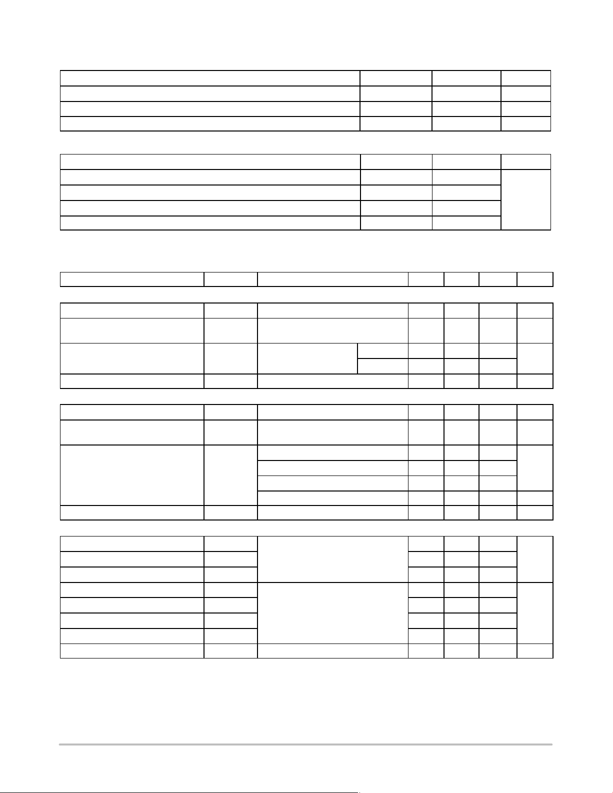
TYPICAL PERFORMANCE CURVES (T
5
4
3
2
1
, DRAIN CURRENT (AMPS)
D
I
0
0521
V
0.07
VGS = 4.5 V
0.06
0.05
0.04
0.03
, DRAIN−TO−SOURCE RESISTANCE (W)
0.02
DS(on)
1.0
R
Figure 3. On−Resistance versus Drain Current
VGS = 1.7 V to 8 V
3
, DRAIN−TO−SOURCE VOLTAGE (VOLTS)
DS
Figure 1. On−Region Characteristics Figure 2. Transfer Characteristics
TJ = 100°C
TJ = 25°C
TJ = −55°C
2.01.5
ID, DRAIN CURRENT (AMPS)
TJ = 25°C
1.6 V
1.5 V
1.4 V
1.3 V
1.2 V
4
2.5
= 25°C unless otherwise noted)
J
6
VDS ≥ 10 V
4
2
, DRAIN CURRENT (AMPS)
D
I
TJ = 25°C
TJ = 100°C
0
0
, GATE−TO−SOURCE VOLTAGE (VOLTS)
V
GS
0.14
TJ = 25°C
0.13
0.12
0.11
0.1
0.09
0.08
0.07
0.06
, DRAIN−TO−SOURCE RESISTANCE (W)
0.05
0.04
DS(on)
1
R
ID, DRAIN CURRENT (AMPS)
Figure 4. On−Resistance versus Drain Current
TJ = −55°C
1
1.5
VGS = 1.8 V
VGS = 2.5 V
VGS = 4.5 V
32
and Gate Voltage
20.5
2.5
3
45
1.6
ID = 2 A
V
= 4.5 V
GS
1.4
1.2
1.0
(NORMALIZED)
0.8
, DRAIN−TO−SOURCE RESISTANCE
0.6
DS(on)
−50 50250−25 75 125100
R
TJ, JUNCTION TEMPERATURE (°C)
Figure 5. On−Resistance Variation with
Temperature
100,000
10,000
1000
, LEAKAGE (nA)
DSS
I
100
150
10
http://onsemi.com
4
VGS = 0 V
TJ = 150°C
TJ = 100°C
21210 304
6 8 14 16 18 22 24 26 28
20
VDS, DRAIN−TO−SOURCE VOLTAGE (VOLTS)
Figure 6. Drain−to−Source Leakage Current
versus Voltage

NTLJF4156N
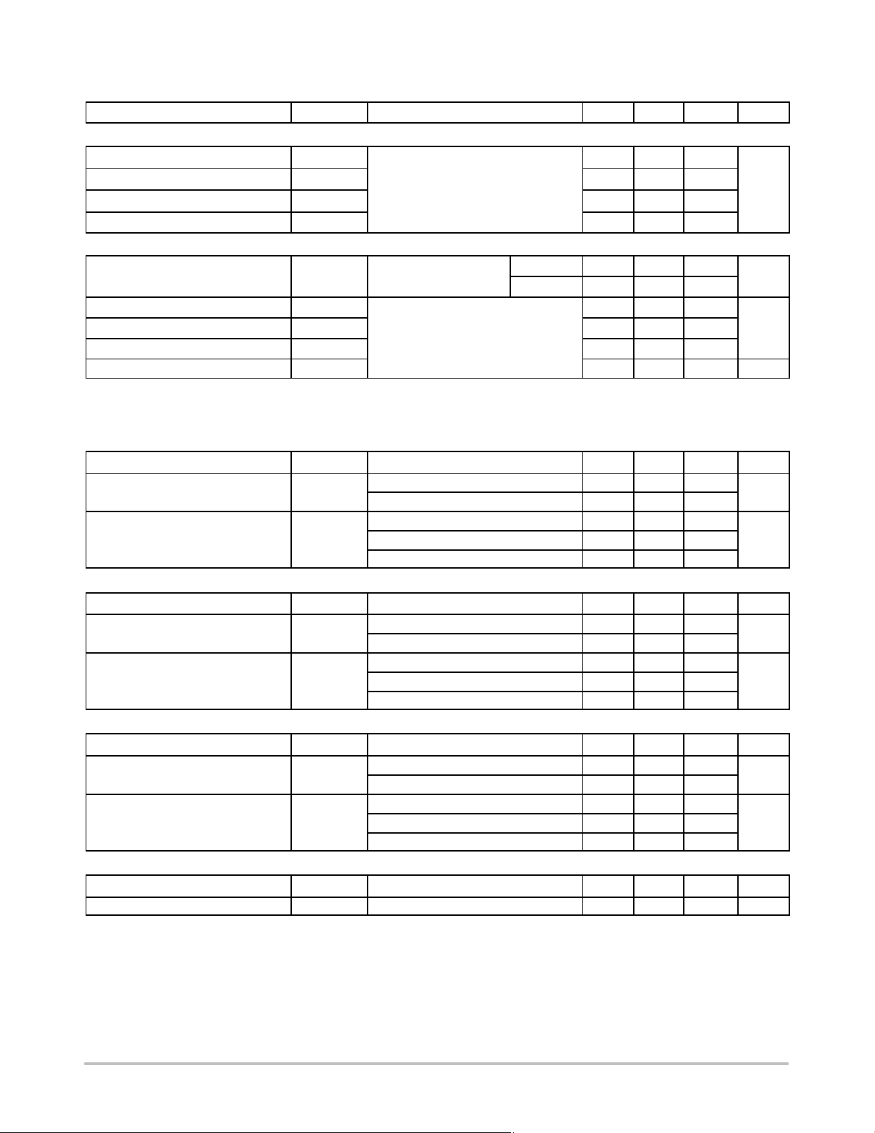
TYPICAL PERFORMANCE CURVES (T
1000
VDS = VGS = 0 V
800
600
C
iss
400
C
rss
C, CAPACITANCE (pF)
200
C
oss
0
010
5 5 15 20 25
V
GS
V
DS
GATE−TO−SOURCE OR DRAIN−TO−SOURCE VOLTAGE (VOLTS)
Figure 7. Capacitance Variation
1000
VDD = 15 V
I
= 2.0 A
D
= 4.5 V
V
GS
100
t, TIME (ns)
10
TJ = 25°C
t
d(off)
t
f
t
r
t
d(on)
30
= 25°C unless otherwise noted)
J
5
QT
4
V
DS
3
Q
GS
2
Q
GD
1
, GATE−TO−SOURCE VOLTAGE (VOLTS)
V
GS
0
0
123
ID = 2.0 A
T
QG, TOTAL GATE CHARGE (nC)
Figure 8. Gate−T o−Source and Drain−To−Source
V oltage versus Total Charge
3
VGS = 0 V
TJ = 150°C
2
1
TJ = 125°C
V
GS
= 25°C
J
54
TJ = 25°C
V
18
DS
, DRAIN−TO−SOURCE VOLTAGE (VOLTS)
15
12
9
6
3
0
6
1
1 10 100
RG, GATE RESISTANCE (OHMS)
Figure 9. Resistive Switching Time
Variation versus Gate Resistance
100
VGS = 4.5 V
SINGLE PULSE
TC = 25°C
10
1
0.1
, DRAIN CURRENT (AMPS)
D
I
0.01
0.1 1 100
V
DS
R
DS(on)
THERMAL LIMIT
PACKAGE LIMIT
, DRAIN−TO−SOURCE VOLTAGE (VOLTS)
Figure 11. Maximum Rated Forward Biased
Safe Operating Area
LIMIT
, SOURCE CURRENT (AMPS)
S
I
0
0.3
, SOURCE−TO−DRAIN VOLTAGE (VOLTS)
V
SD
0.6
Figure 10. Diode Forward Voltage versus Current
10 ms
100 ms
1 ms
10 ms
dc
10
0.9
http://onsemi.com
5

NTLJF4156N
1000
D = 0.5
100
0.2
0.1
10
0.05
0.02
(NORMALIZED)
0.01
1
0.1
r(t), EFFECTIVE TRANSIENT THERMAL RESISTANCE
TYPICAL PERFORMANCE CURVES (T
SINGLE PULSE
t, TIME (ms)
Figure 12. Thermal Response
= 25°C unless otherwise noted)
J
P
(pk)
t
1
t
2
DUTY CYCLE, D = t1/t
R
(t) = r(t) R
q
JC
q
JC
D CURVES APPLY FOR POWER
PULSE TRAIN SHOWN
READ TIME AT t
T
J(pk)
2
10.010.00001
− TC = P
(pk)
1
R
q
JC
100 1000100.10.0010.00010.000001
(t)
http://onsemi.com
6

NTLJF4156N
10
)
10
.9
0
TYPICAL SCHOTTKY PERFORMANCE CURVES (T
1.0
0.1
, INSTANTANEOUS FORWARD CURRENT (AMPS
F
I
1.0E+0
100E−3
TJ = 85°C
TJ = 125°C
TJ = 25°C
TJ = −55°C
0.1 0.2 0.4
VF, INSTANTANEOUS FORWARD VOLTAGE (VOLTS)
0.6 0.8
Figure 13. Typical Forward Voltage Figure 14. Maximum Forward Voltage
= 25°C unless otherwise noted)
J
1.0
TJ = 85°C
TJ = 125°C
0.1
, INSTANTANEOUS FORWARD CURRENT (AMPS)
0.90.70.3 0.5
F
I
1.0E+0
100E−3
VF, MAXIMUM FORWARD VOLTAGE (VOLTS)
TJ = 25°C
TJ = 125°C
0.6 0.80.1 0.2 0.4
0.70.3 0.5
0
10E−3
1.0E−3
100E−6
10E−6
, REVERSE CURRENT (AMPS)
R
I
1.0E−6
100E−9
0
V
, REVERSE VOLTAGE (VOLTS)
R
TJ = 125°C
TJ = 85°C
TJ = 25°C
10 20
30
10E−3
1.0E−3
100E−6
10E−6
1.0E−6
R
I , MAXIMUM REVERSE CURRENT (AMPS)
100E−9
TJ = 85°C
TJ = 25°C
0
10 20 3
, REVERSE VOLTAGE (VOLTS)
V
R
Figure 15. Typical Reverse Current Figure 16. Maximum Reverse Current
http://onsemi.com
7

NTLJF4156N
ORDERING INFORMATION
Device Package Shipping
NTLJF4156NT1G SC−88FL
(Pb−Free)
†For information on tape and reel specifications, including part orientation and tape sizes, please refer to our Tape and Reel Packaging
Specifications Brochure, BRD8011/D.
3000 / Tape & Reel
†
http://onsemi.com
8

6X
2X
2X
PIN ONE
REFERENCE
0.10 C
0.10 C
0.10 C
0.08 C
6X
L
D3
NTLJF4156N
PACKAGE DIMENSIONS
DFN6
CASE 506AN−01
ISSUE A
D
A
B
E
STYLE 1:
PIN 1. SOURCE1
2. GATE1
3. DRAIN2
A3
4. SOURCE2
5. GATE2
6. DRAIN1
A
A1
SEATING
C
PLANE
D2
4X
1
3
e
NOTES:
1. DIMENSIONING AND TOLERANCING PER
ASME Y14.5M, 1994.
2. CONTROLLING DIMENSION: MILLIMETERS.
3. DIMENSION b APPLIES TO PLATED
TERMINAL AND IS MEASURED BETWEEN
0.15 AND 0.20mm FROM TERMINAL.
4. COPLANARITY APPLIES TO THE EXPOSED
PAD AS WELL AS THE TERMINALS.
MILLIMETERS
DIMAMIN MAX
0.70 0.80
A1 0.00 0.05
A3 0.20 REF
b 0.25 0.35
D 2.00 BSC
D2 0.57 0.77
2.00 BSC
E
E2
0.90 1.10
e
0.65 BSC
0.25 REF
K
L
J
0.20
0.15 REF
0.30
SOLDERING FOOTPRINT*
6X
0.770
0.0303
0.475
0.0187
6X
0.325
0.0128
E2
2X
0.200
0.0079
0.650
0.0256
6X
K
6
J6X
BOTTOM VIEW
4
b
6X
A0.10 C
B
0.05 C
NOTE 3
0.770
0.0303
2.300
PITCH
1.100
0.0433
0.0906
inches
*For additional information on our Pb−Free strategy and soldering
details, please download the ON Semiconductor Soldering and
Mounting Techniques Reference Manual, SOLDERRM/D.
mCool is a trademark of Semiconductor Components Industries, LLC (SCILLC).
ON Semiconductor and are registered trademarks of Semiconductor Components Industries, LLC (SCILLC). SCILLC reserves the right to make changes without further notice
to any products herein. SCILLC makes no warranty, representation or guarantee regarding the suitability of its products for any particular purpose, nor does SCILLC assume any liability
arising out of the application or use of any product or circuit, and specifically disclaims any and all liability, including without limitation special, consequential or incidental damages.
“Typical” parameters which may be provided in SCILLC data sheets and/or specifications can and do vary in different applications and actual performance may vary over time. All
operating parameters, including “Typicals” must be validated for each customer application by customer’s technical experts. SCILLC does not convey any license under its patent rights
nor the rights of others. SCILLC products are not designed, intended, or authorized for use as components in systems intended for surgical implant into the body, or other applications
intended to support or sustain life, or for any other application in which the failure of the SCILLC product could create a situation where personal injury or death may occur. Should
Buyer purchase or use SCILLC products for any such unintended or unauthorized application, Buyer shall indemnify and hold SCILLC and its officers, employees, subsidiaries, affiliates,
and distributors harmless against all claims, costs, damages, and expenses, and reasonable attorney fees arising out of, directly or indirectly, any claim of personal injury or death
associated with such unintended or unauthorized use, even if such claim alleges that SCILLC was negligent regarding the design or manufacture of the part. SCILLC is an Equal
Opportunity/Affirmative Action Employer. This literature is subject to all applicable copyright laws and is not for resale in any manner.
mm
PUBLICATION ORDERING INFORMATION
LITERATURE FULFILLMENT:
Literature Distribution Center for ON Semiconductor
P.O. Box 61312, Phoenix, Arizona 85082−1312 USA
Phone: 480−829−7710 or 800−344−3860 Toll Free USA/Canada
Fax: 480−829−7709 or 800−344−3867 Toll Free USA/Canada
Email: orderlit@onsemi.com
N. American Technical Support: 800−282−9855 Toll Free
USA/Canada
Japan: ON Semiconductor, Japan Customer Focus Center
2−9−1 Kamimeguro, Meguro−ku, Tokyo, Japan 153−0051
Phone: 81−3−5773−3850
http://onsemi.com
9
ON Semiconductor Website: http://onsemi.com
Order Literature: http://www.onsemi.com/litorder
For additional information, please contact your
local Sales Representative.
NTLJF4156N/D
 Loading...