

查询NTHD5903T1供应商
NTHD5903T1
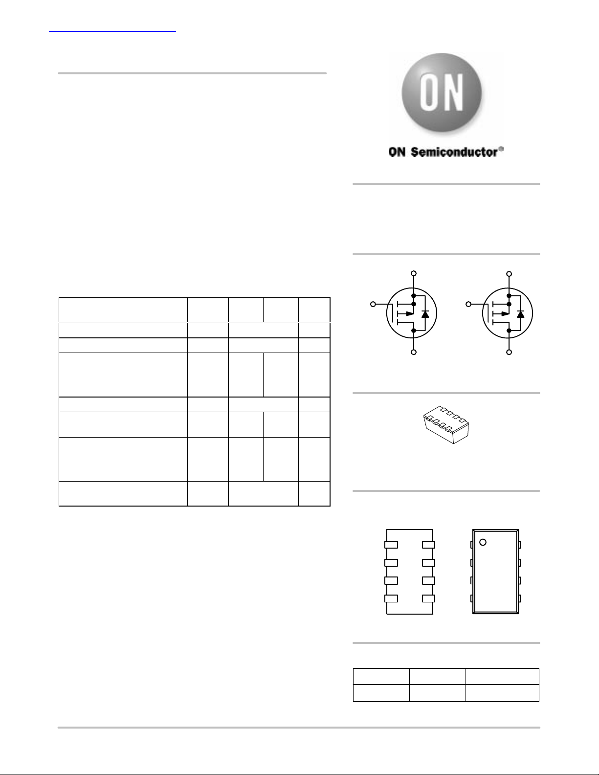
Power MOSFET
Dual P-Channel ChipFET
2.1 Amps, 20 Volts
Features
• Low R
• Logic Level Gate Drive
• Miniature ChipFET Surface Mount Package Saves Board Space
Applications
• Power Management in Portable and Battery–Powered Products; i.e.,
Cellular and Cordless T elephones and PCMCIA Cards
for Higher Efficiency
DS(on)
http://onsemi.com
DUAL P–CHANNEL
2.1 AMPS, 20 VOLTS
R
DS(on)
= 155 m
MAXIMUM RATINGS (T
Rating
Drain–Source Voltage V
Gate–Source Voltage V
Continuous Drain Current
(T
= 150°C) (Note 1)
J
= 25°C
T
A
T
= 85°C
A
Pulsed Drain Current I
Continuous Source Current
(Diode Conduction) (Note 1)
Maximum Power Dissipation
(Note 1)
= 25°C
T
A
T
= 85°C
A
Operating Junction and Storage
Temperature Range
1. Surface Mounted on 1″ x 1″ FR4 Board.
= 25°C unless otherwise noted)
A
Symbol 5 secs
TJ, T
P
DS
GS
I
D
DM
I
S
1
Steady
State
–20 V
12 V
2.9
2.1
S
D
–1.8 –0.9 A
2.1
1.1
stg
2.1
1.5
10 A
1.1
0.6
–55 to +150 °C
Unit
A
W
G
1
D
G
2
1
P–Channel MOSFETP–Channel MOSFET
ChipFET
CASE 1206A
STYLE 2
PIN CONNECTIONS
8
D
1
7
D
1
6
D
2
D
2
1
S
1
1
2
3
45
2
G
1
S
3
2
4
G
2
S
2
MARKING
DIAGRAM
A7
D
2
8
7
6
5
Semiconductor Components Industries, LLC, 2002
March, 2002 – Rev . 2
A7 = Specific Device Code
ORDERING INFORMATION
Device Package Shipping
NTHD5903T1 ChipFET 3000/Tape & Reel
1 Publication Order Number:
NTHD5903T1/D
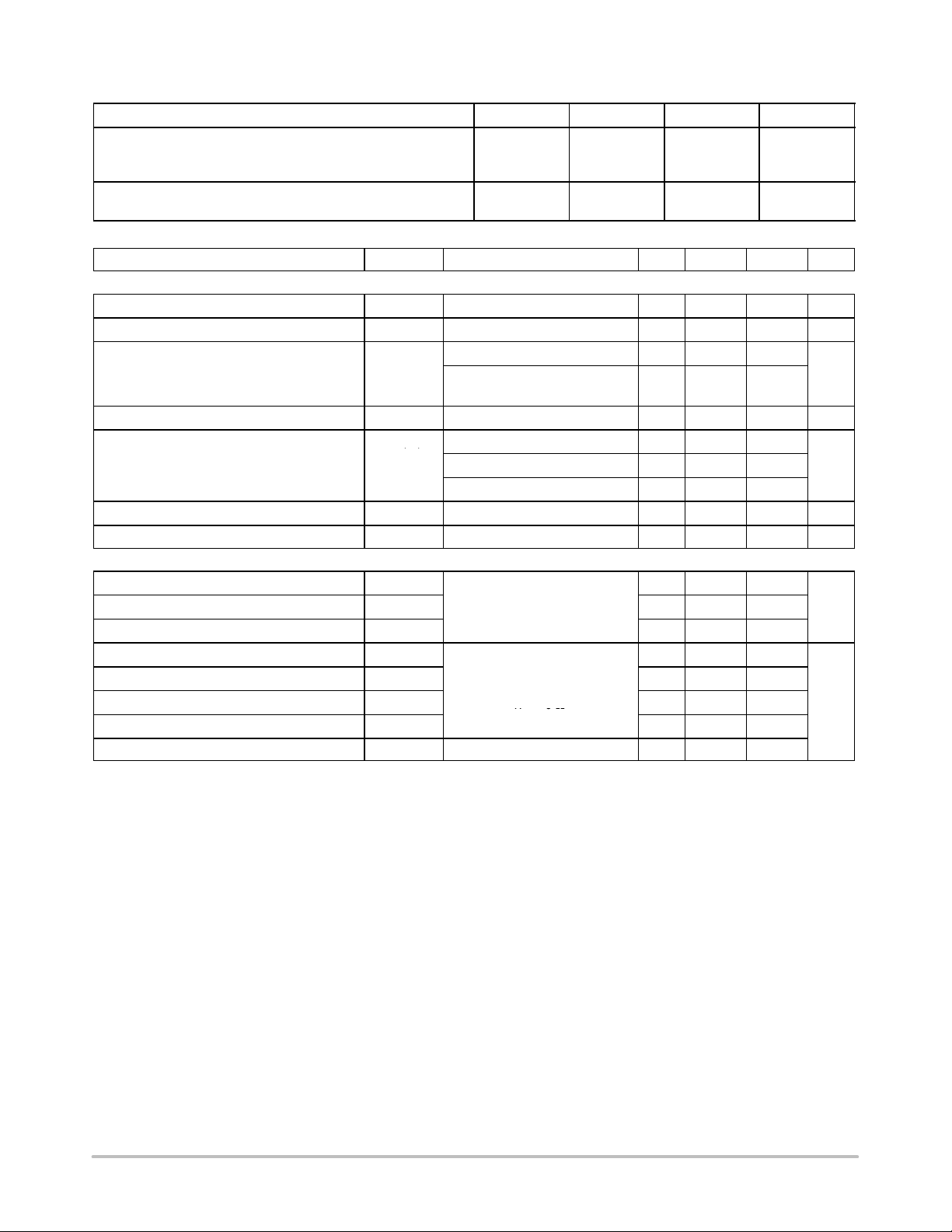
THERMAL CHARACTERISTICS
()
I
A
R
G
Characteristic Symbol Typ Max Unit
Maximum Junction–to–Ambient (Note 2)
t 5 sec
Steady State
Maximum Junction–to–Foot (Drain)
Steady State
ELECTRICAL CHARACTERISTICS (T
Characteristic
Static
Gate Threshold Voltage
Gate–Body Leakage I
Zero Gate Voltage Drain Current I
On–State Drain Current (Note 3) I
Drain–Source On–State Resistance (Note 3) r
Forward Transconductance (Note 3) g
Diode Forward Voltage (Note 3) V
Dynamic (Note 4)
Total Gate Charge
Gate–Source Charge Q
Gate–Drain Charge Q
Turn–On Delay Time t
Rise Time t
Turn–Off Delay Time t
Fall Time t
Source–Drain Reverse Recovery Time t
2. Surface Mounted on 1″ x 1″ FR4 Board.
3. Pulse Test: Pulse Width 300 s, Duty Cycle 2%.
4. Guaranteed by design, not subject to production testing.
= 25°C unless otherwise noted)
J
Symbol Test Condition Min Typ Max Unit
V
GS(th)
GSS
DSS
D(on)
DS(on)
fs
SD
Q
g
gs
gd
d(on)
r
d(off)
f
rr
NTHD5903T1
R
thJA
R
thJF
VDS = VGS, ID = –250 A –0.6 – – V
VDS = 0 V, VGS = 12 V – – 100 nA
VDS = –16 V, VGS = 0 V – – –1.0
VDS = –16 V, VGS = 0 V,
T
= 85°C
J
VDS –5.0 V, VGS = –4.5 V –10 – – A
VGS = –4.5 V, ID = –2.1 A – 0.130 0.155
VGS = –3.6 V, ID = –2.0 A – 0.150 0.180
VGS = –2.5 V, ID = –1.7 A – 0.215 0.260
VDS = –10 V, ID = –2.1 A – 5.0 – S
IS = –0.9 A, VGS = 0 V – –0.8 –1.2 V
VDS = –10 V, VGS = –4.5 V,
I
= –2.1 A
= –2.1
D
VDD = –10 V, RL = 10
ID –1.0 A, V
R
= 6
6
G
GEN
IF = –0.9 A, di/dt = 100 A/s
50
90
60
110
30 40 °C/W
– – –5.0
– 3.0 6.0
– 0.9 –
– 0.6 –
– 13 20
= –4.5 V,
– 35 55
– 25 40
– 25 40
– 40 80
°C/W
A
nC
ns
http://onsemi.com
2
NTHD5903T1
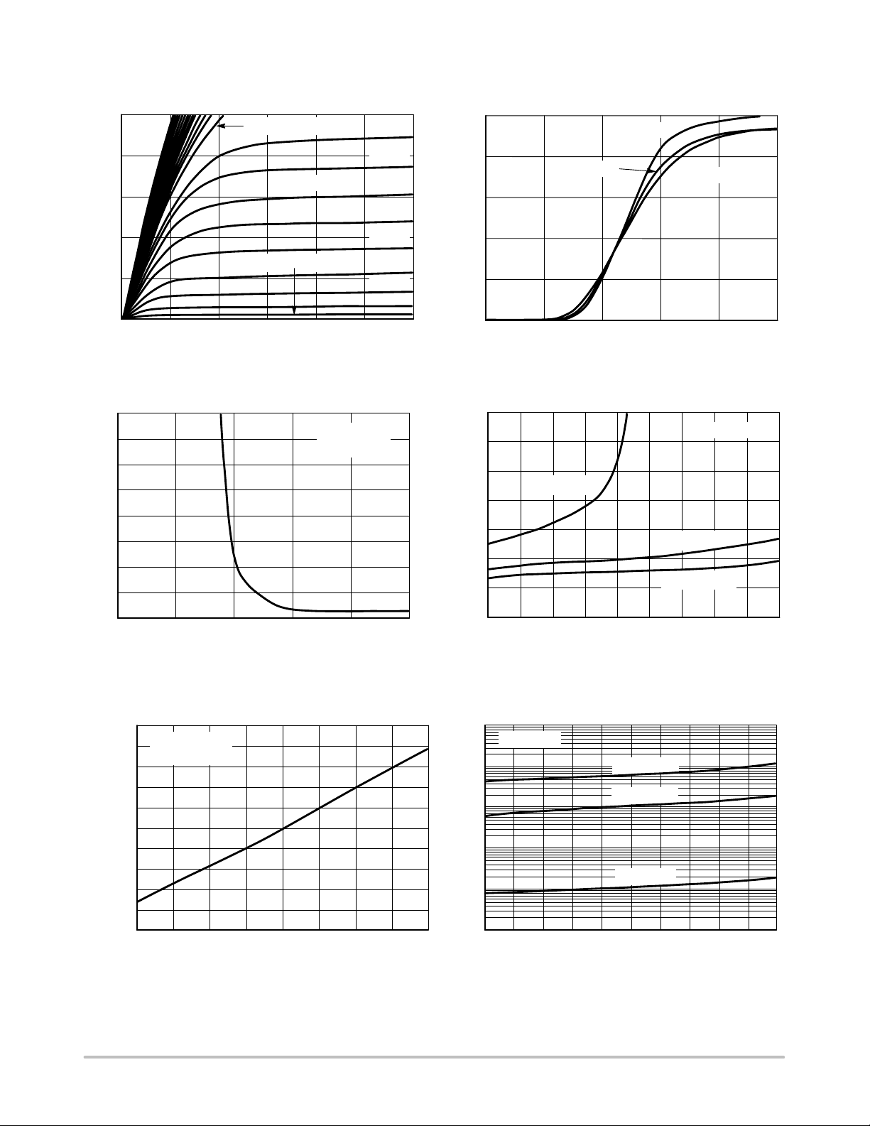
TYPICAL ELECTRICAL CHARACTERISTICS
10
VGS = 4 V – 10 V
8
TJ = 25°C
6
3.6 V
3.4 V
3 V
10
125°C
8
25°C
6
2.8 V
4
DRAIN CURRENT (AMPS)
2
D,
I
0
0
1
–V
, DRAIN–TO–SOURCE VOLTAGE (VOLTS)
DS
Figure 1. On–Region Characteristics
4
3
VGS = 1.4 V
4
ID = –2.1 A
T
= 25°C
J
5
2.6 V
2.4 V
2.2 V
1.8 V
632
4
DRAIN CURRENT (AMPS)
2
D,
I
0
0
1
VGS, GATE–TO–SOURCE VOLTAGE (VOLTS)
Figure 2. Transfer Characteristics
0.4
0.35
0.3
VGS = –2.5 V
0.25
2
0.2
1
DRAIN–TO–SOURCE RESISTANCE ()
0
05
DS(on),
R
13
24
–VGS, GATE–TO–SOURCE VOLTAGE (VOLTS)
0.15
0.1
DRAIN–TO–SOURCE RESISTANCE ()
0.05
DS(on),
191085
R
4
–ID, DRAIN CURRENT (AMPS)
TC = –55°C
324
5
TJ = 25°C
VGS = –3.6 V
VGS = –4.5 V
7623
Figure 3. On–Resistance vs. Gate–to–Source
Voltage
1.6
ID = –2.1 A
V
= –4.5 V
1.4
GS
1.2
1
DRAIN–TO–SOURCE
0.8
DS(on),
R
RESISTANCE (NORMALIZED)
0.6
–50 0–25 25
75 150
50 125100
TJ, JUNCTION TEMPERATURE (°C)
Figure 5. On–Resistance Variation with
Temperature
1.0E–6
1.0E–7
1.0E–8
, LEAKAGE (A)
1.0E–9
DSS
I
1.0E–10
1.0E–11
http://onsemi.com
3
Figure 4. On–Resistance vs. Drain Current and
Gate Voltage
VGS = 0 V
TJ = 150°C
TJ = 100°C
TJ = 25°C
04 8
12
–VDS, DRAIN–TO–SOURCE VOLTAGE (VOLTS)
Figure 6. Drain–to–Source Leakage Current
vs. Voltage
2016

NTHD5903T1
TYPICAL ELECTRICAL CHARACTERISTICS
600
C
VDS = 0 V VGS = 0 V
iss
TJ = 25°C
500
400
C
rss
300
200
C
C, CAPACITANCE (pF)
oss
100
0
–4 16
–8 0
VGSV
DS
84–12 12
20
GATE–TO–SOURCE OR DRAIN–TO–SOURCE VOLTAGE (VOLTS)
Figure 7. Capacitance Variation
100
VDD = –10 V
I
= –1.0 A
D
V
GS
10
t, TIME (ns)
= –4.5 V
t
d(off)
t
f
t
r
t
d(on)
6
QT
5
–V
DS
4
–V
GS
3
Q2Q1
2
1
GATE–TO–SOURCE VOLTAGE (VOLTS)
0
02
GS,
–V
14
1.50.5 3.5
Qg, TOTAL GATE CHARGE (nC)
ID = –2.1 A
= 25°C
T
J
32.5
Figure 8. Gate–to–Source and
Drain–to–Source Voltage vs. Total Charge
5
VGS = 0 V
T
= 25°C
J
4
3
2
6
5
4
3
2
1
0
DRAIN–TO–SOURCE VOLTAGE (VOLTS)
DS,
–V
1
Figure 9. Resistive Switching Time Variation
2
1
Duty Cycle = 0.5
0.2
0.1
0.1
0.05
0.02
Thermal Impedance
Normalized Effective Transient
0.01
–4 –3 –2 –1
10 1010
1
, SOURCE CURRENT (AMPS)
S
I
0
101
, GATE RESISTANCE (OHMS)
R
G
100
, SOURCE–TO–DRAIN VOLTAGE (VOLTS)
V
SD
Figure 10. Diode Forward Voltage vs. Current
vs. Gate Resistance
Notes:
1. Duty Cycle, D =
2. Per Unit Base = R
3. T
Single Pulse
JM –
4. Surface Mounted
10 1 10 100 600
Square Wave Pulse Duration (sec)
Figure 11. Normalized Thermal Transient Impedance, Junction–to–Ambient
P
DM
TA = PDMZ
t
1
0.80
t
t
t
thJA
2
1
2
= 90°C/W
thJA
(t)
1.2
10.60.40.2
http://onsemi.com
4

Notes
NTHD5903T1
http://onsemi.com
5

Notes
NTHD5903T1
http://onsemi.com
6

NTHD5903T1
PACKAGE DIMENSIONS
ChipFET
CASE 1206A–03
ISSUE D
A
8765
BS
1234
L
D
G
C
M
J
0.05 (0.002)
K
8765
1234
STYLE 2:
PIN 1. SOURCE 1
2. GATE 1
3. SOURCE 2
4. GATE 2
5. DRAIN 2
6. DRAIN 2
7. DRAIN 1
8. DRAIN 1
NOTES:
1. DIMENSIONING AND TOLERANCING PER ANSI
Y14.5M, 1982.
2. CONTROLLING DIMENSION: MILLIMETER.
3. MOLD GATE BURRS SHALL NOT EXCEED 0.13 MM
PER SIDE.
4. LEADFRAME TO MOLDED BODY OFFSET IN
HORIZONTAL AND VERTICAL SHALL NOT EXCEED
0.08 MM.
5. DIMENSIONS A AND B EXCLUSIVE OF MOLD GATE
BURRS.
6. NO MOLD FLASH ALLOWED ON THE TOP AND
BOTTOM LEAD SURFACE.
7. 1206A-01 AND 1206A-02 OBSOLETE. NEW
STANDARD IS 1206A-03.
2.00
INCHESMILLIMETERS
0.072 0.080
DIM MIN MAX MIN MAX
A 2.95 3.10 0.116 0.122
B 1.55 1.70 0.061 0.067
C 1.00 1.10 0.039 0.043
D 0.25 0.35 0.010 0.014
G 0.65 BSC 0.025 BSC
J 0.10 0.20 0.004 0.008
K 0.28 0.42 0.011 0.017
L 0.55 BSC 0.022 BSC
M °5 NOM
°5 NOM
S 1.80
http://onsemi.com
7

NTHD5903T1
ChipFET is a trademark of Vishay Siliconix.
ON Semiconductor is a trademark and is a registered trademark of Semiconductor Components Industries, LLC (SCILLC). SCILLC reserves the right
to make changes without further notice to any products herein. SCILLC makes no warranty, representation or guarantee regarding the suitability of its products
for any particular purpose, nor does SCILLC assume any liability arising out of the application or use of any product or circuit, and specifically disclaims any
and all liability, including without limitation special, consequential or incidental damages. “Typical” parameters which may be provided in SCILLC data sheets
and/or specifications can and do vary in different applications and actual performance may vary over time. All operating parameters, including “Typicals” must
be validated for each customer application by customer’s technical experts. SCILLC does not convey any license under its patent rights nor the rights of others.
SCILLC products are not designed, intended, or authorized for use as components in systems intended for surgical implant into the body, or other applications
intended to support or sustain life, or for any other application in which the failure of the SCILLC product could create a situation where personal injury or death
may occur. Should Buyer purchase or use SCILLC products for any such unintended or unauthorized application, Buyer shall indemnify and hold SCILLC
and its officers, employees, subsidiaries, affiliates, and distributors harmless against all claims, costs, damages, and expenses, and reasonable attorney fees
arising out of, directly or indirectly, any claim of personal injury or death associated with such unintended or unauthorized use, even if such claim alleges that
SCILLC was negligent regarding the design or manufacture of the part. SCILLC is an Equal Opportunity/Affirmative Action Employer.
PUBLICATION ORDERING INFORMATION
Literature Fulfillment:
Literature Distribution Center for ON Semiconductor
P.O. Box 5163, Denver, Colorado 80217 USA
Phone: 303–675–2175 or 800–344–3860 Toll Free USA/Canada
Fax: 303–675–2176 or 800–344–3867 Toll Free USA/Canada
Email: ONlit@hibbertco.com
N. American Technical Support: 800–282–9855 Toll Free USA/Canada
http://onsemi.com
JAPAN: ON Semiconductor, Japan Customer Focus Center
4–32–1 Nishi–Gotanda, Shinagawa–ku, Tokyo, Japan 141–0031
Phone: 81–3–5740–2700
Email: r14525@onsemi.com
ON Semiconductor Website: http://onsemi.com
For additional information, please contact your local
Sales Representative.
NTHD5903T1/D
8
 Loading...