

查询NTGS3441T1供应商
NTGS3441T1
Power MOSFET
1 Amp, 20 Volts
P−Channel TSOP−6
Features
• Ultra Low R
DS(on)
• Higher Efficiency Extending Battery Life
• Miniature TSOP−6 Surface Mount Package
• Pb−Free Package is Available
Applications
• Power Management in Portable and Battery−Powered Products, i.e.:
Cellular and Cordless T elephones, and PCMCIA Cards
MAXIMUM RATINGS (T
Drain−to−Source Voltage V
Gate−to−Source Voltage − Continuous V
Thermal Resistance
Junction−to−Ambient (Note 1)
Total Power Dissipation @ T
Drain Current − Continuous @ T
− Pulsed Drain Current (T
Thermal Resistance
Junction−to−Ambient (Note 2)
Total Power Dissipation @ T
Drain Current − Continuous @ T
− Pulsed Drain Current (T
Thermal Resistance
Junction−to−Ambient (Note 3)
Total Power Dissipation @ T
Drain Current − Continuous @ T
− Pulsed Drain Current (T
Operating and Storage Temperature Range TJ, T
Maximum Lead Temperature for Soldering
Purposes for 10 Seconds
1. Minimum FR−4 or G−10PCB, operating to steady state.
2. Mounted onto a 2″ square FR−4 board (1″ sq. 2 oz. cu. 0.06″ thick single
sided), operating to steady state.
3. Mounted onto a 2″ square FR−4 board (1″ sq. 2 oz. cu. 0.06″ thick single
sided), t 5.0 seconds.
= 25°C unless otherwise noted)
J
Rating
= 25°C
A
= 25°C
A
10 S)
p
= 25°C
A
= 25°C
A
10 S)
p
= 25°C
A
= 25°C
A
10 S)
p
Symbol Value Unit
−20 V
8.0 V
244
0.5
−1.65
−10
128
1.0
−2.35
−14
62.5
2.0
−3.3
−20
−55 to 150 °C
260 °C
°C/W
W
°C/W
W
°C/W
W
A
A
A
A
A
A
R
R
R
DSS
P
I
I
DM
P
I
I
DM
P
I
I
DM
T
GS
JA
d
D
JA
d
D
JA
d
D
stg
L
http://onsemi.com
1 AMPERE
20 VOLTS
R
DS(on)
3
1
PT = Device Code
W = Work Week
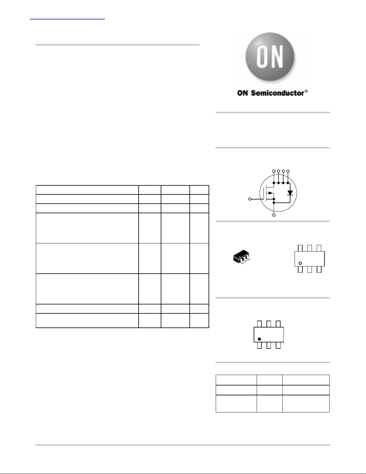
PIN ASSIGNMENT
= 90 m
P−Channel
1256
4
TSOP−6
CASE 318G
STYLE 1
Source
DrainDrain
4
56
321
GateDrain
Drain
MARKING
DIAGRAM
PT
W
1
Semiconductor Components Industries, LLC, 2004
April, 2004 − Rev. 4
ORDERING INFORMATION
Device Package Shipping
NTGS3441T1 TSOP−6 3000 / Tape & Reel
NTGS3441T1G TSOP−6
(Pb−Free)
†For information on tape and reel specifications,
including part orientation and tape sizes, please
refer to our Tape and Reel Packaging Specifications
Brochure, BRD8011/D.
1 Publication Order Number:
3000 / Tape& Reel
NTGS3441T1/D
†
NTGS3441T1
)
f = 1.0 MHz)
(
(V
DD
−20 Vdc, I
D
Adc
)
I
D
Adc)
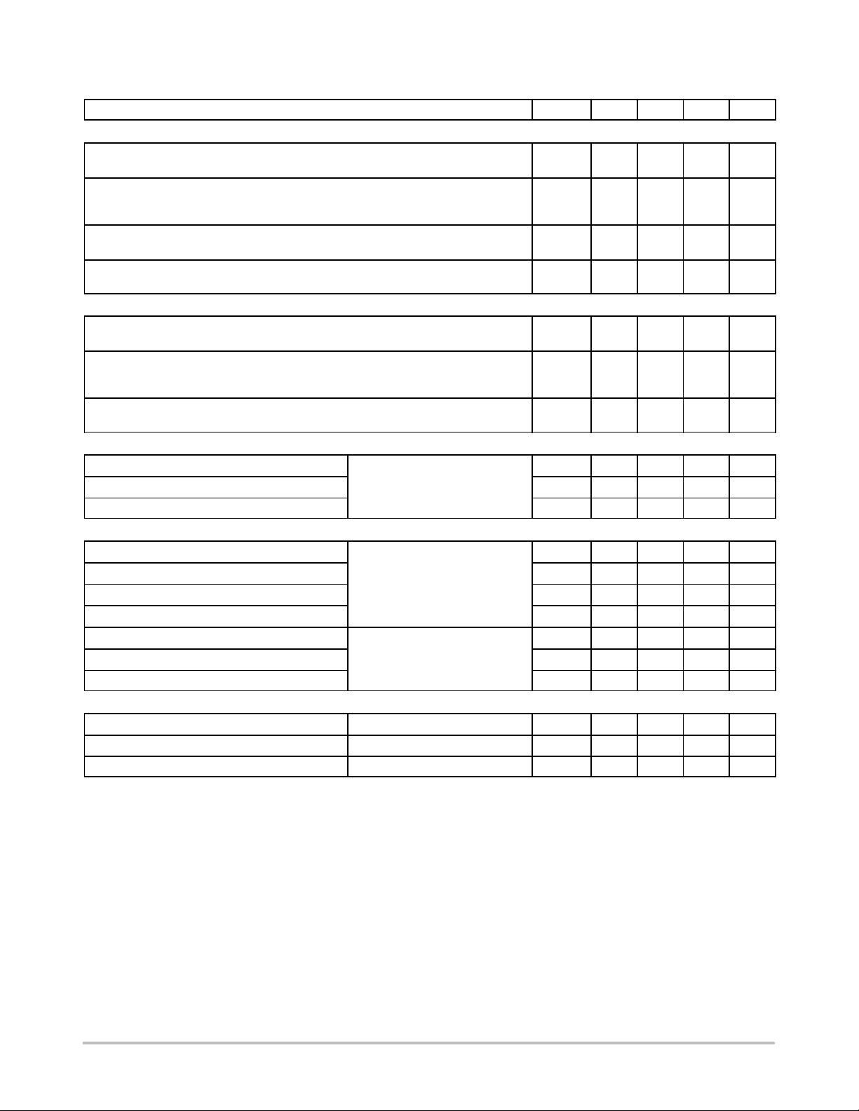
ELECTRICAL CHARACTERISTICS (T
= 25°C unless otherwise noted) (Notes 4 & 5)
A
Characteristic
OFF CHARACTERISTICS
Drain−Source Breakdown Voltage
= 0 Vdc, ID = −10 A)
(V
GS
Zero Gate Voltage Drain Current
(VGS = 0 Vdc, VDS = −20 Vdc, TJ = 25°C)
(V
= 0 Vdc, VDS = −20 Vdc, TJ = 70°C)
GS
Gate−Body Leakage Current
(VGS = −8.0 Vdc, VDS = 0 Vdc)
Gate−Body Leakage Current
(VGS = +8.0 Vdc, VDS = 0 Vdc)
ON CHARACTERISTICS
Gate Threshold Voltage
= VGS, ID = −250 Adc)
(V
DS
Static Drain−Source On−State Resistance
(VGS = −4.5 Vdc, ID = −3.3 Adc)
(V
= −2.5 Vdc, ID = −2.9 Adc)
GS
Forward Transconductance
(VDS = −10 Vdc, ID = −3.3 Adc)
DYNAMIC CHARACTERISTICS
Input Capacitance
Output Capacitance
(VDS = −5.0 Vdc, VGS = 0 Vdc,
f = 1.0 MHz
Reverse Transfer Capacitance
SWITCHING CHARACTERISTICS
Turn−On Delay Time
Rise Time
Turn−Off Delay Time
V
= −20 Vdc, I
=
= −1.6 Adc,
= −1.6
VGS = −4.5 Vdc, Rg = 6.0 )
,
Fall Time t
Total Gate Charge Q
Gate−Source Charge
(VDS = −10 Vdc, VGS = −4.5 Vdc,
= −3.3
I
= −3.3 Adc
Gate−Drain Charge
BODY−DRAIN DIODE RATINGS
Diode Forward On−Voltage (IS = −1.6 Adc, VGS = 0 Vdc) V
Diode Forward On−Voltage (IS = −3.3 Adc, VGS = 0 Vdc) V
Reverse Recovery Time (IS = −1.6 Adc, dIS/dt = 100 A/s) t
4. Indicates Pulse Test: P.W. = 300 sec max, Duty Cycle = 2%.
5. Handling precautions to protect against electrostatic discharge is mandatory.
Symbol Min Typ Max Unit
V
(BR)DSS
I
DSS
I
GSS
I
GSS
V
GS(th)
R
DS(on)
g
C
C
C
t
d(on)
t
d(off)
Q
Q
−20 − −
−
−
− − −100
− − 100
−0.45 −1.05 −1.50
−
−
FS
iss
oss
rss
− 6.8 −
− 480 − pF
− 265 − pF
− 100 − pF
− 13 25 ns
t
r
− 23.5 45 ns
− 27 50 ns
f
tot
gs
gd
SD
SD
rr
− 24 45 ns
− 6.2 14 nC
− 1.3 − nC
− 2.5 − nC
− −0.88 −1.2 Vdc
− −0.98 − Vdc
− 30 60 ns
−
−
0.069
0.117
−1.0
−5.0
0.090
0.135
Vdc
Adc
nAdc
nAdc
Vdc
mhos
http://onsemi.com
2
 Loading...