

ON Semiconductor NTF5P03T3 Technical data
NTF5P03T3
l
s
l
Preferred Device
Power MOSFET
5.2 Amps, 30 Volts
P−Channel SOT−223
Features
• Ultra Low R
DS(on)
• Higher Efficiency Extending Battery Life
• Logic Level Gate Drive
• Miniature SOT−223 Surface Mount Package
• Avalanche Energy Specified
• Pb−Free Package is Available
Applications
• DC−DC Converters
• Power Management
• Motor Controls
• Inductive Loads
• Replaces MMFT5P03HD
http://onsemi.com
5.2 AMPERES, 30 VOLTS
= 100 mW
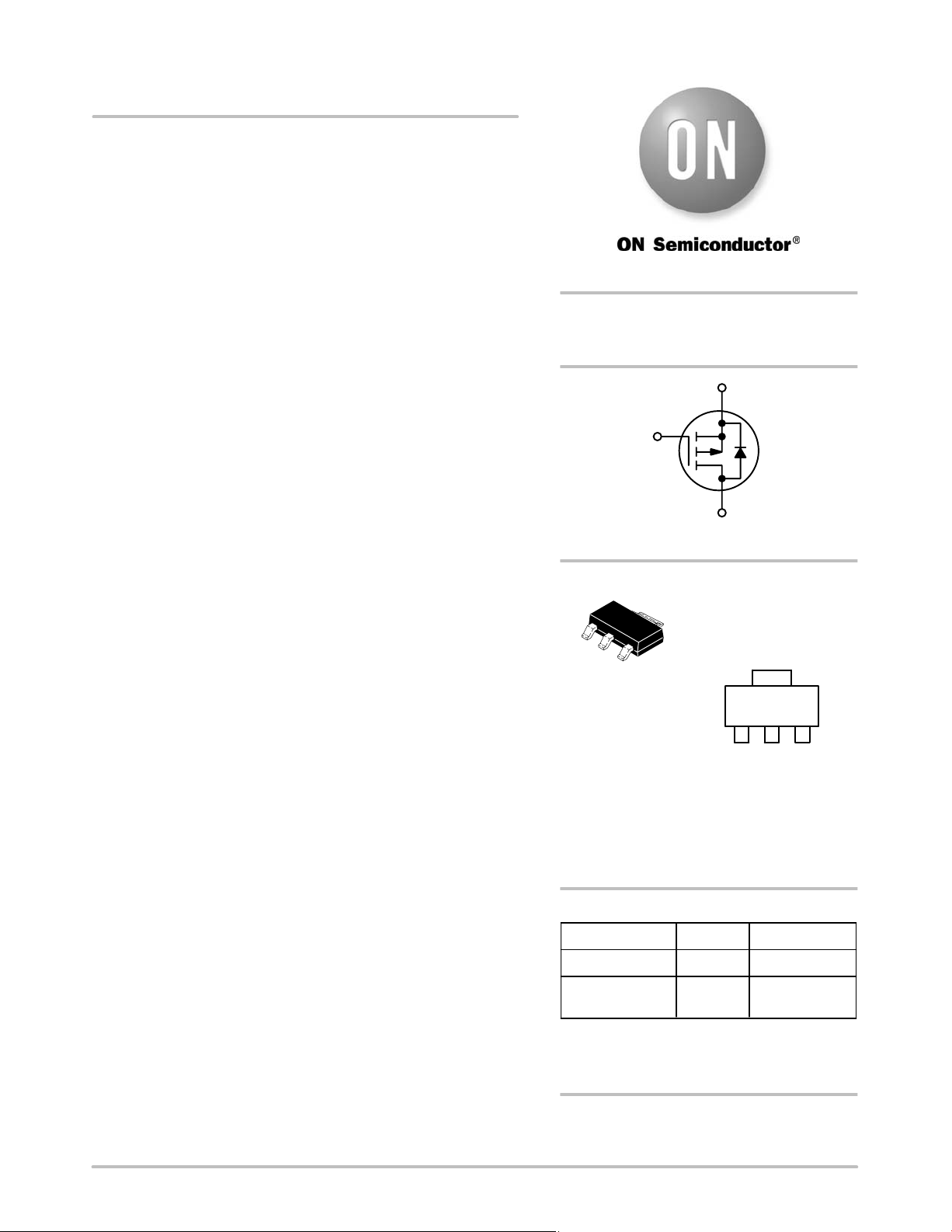
S
D
P−Channel MOSFET
MARKING
4
DIAGRAM
& PIN
ASSIGNMENT
Drain
AYM
5P03 G
1
2
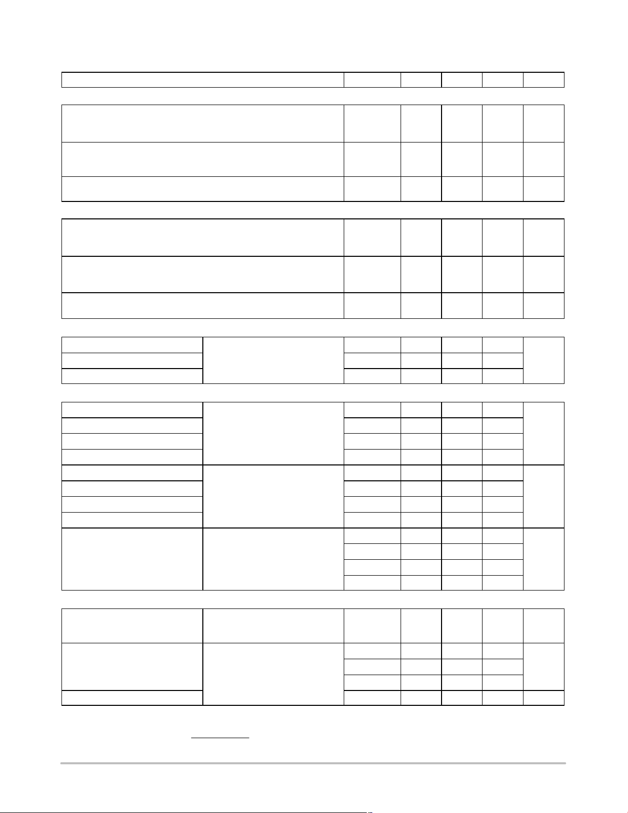
SOT−223
CASE 318E
STYLE 3
3
R
DS(on)
G
4
G
© Semiconductor Components Industries, LLC, 2006
December, 2006 − Rev. 3
1
Gate2Drain3Source
A = Assembly Location
Y = Year
M = Date Code
5P03 = Specific Device Code
G = Pb−Free Package
(Note: Microdot may be in either location)
ORDERING INFORMATION
Device Package Shipping
NTF5P03T3 SOT−223 4000/Tape & Ree
NTF5P03T3G
†For information on tape and reel specifications,
including part orientation and tape sizes, please
refer to our Tape and Reel Packaging Specification
Brochure, BRD801 1/D.
Preferred devices are recommended choices for future use
and best overall value.
1
SOT−223
(Pb−Free)
Publication Order Number:
4000/Tape & Ree
NTF5P03T3/D
†

NTF5P03T3
MAXIMUM RATINGS (T
= 25°C unless otherwise noted)
J
Negative sign for P−Channel devices omitted for clarity
Rating
Drain−to−Source Voltage V
Drain−to−Gate Voltage (RGS = 1.0 MW)
Gate−to−Source Voltage − Continuous V
1 sq in
FR−4 or G−10 PCB
10 seconds
Thermal Resistance − Junction to Ambient
Total Power Dissipation @ T
Linear Derating Factor
Drain Current − Continuous @ T
Continuous @ TA = 70°C
= 25°C
A
A
= 25°C
Pulsed Drain Current (Note 1)
Minimum
FR−4 or G−10 PCB
Thermal Resistance − Junction to Ambient
Total Power Dissipation @ T
= 25°C
A
Linear Derating Factor
10 seconds
Drain Current − Continuous @ T
Continuous @ T
= 70°C
A
= 25°C
A
Pulsed Drain Current (Note 1)
Operating and Storage Temperature Range TJ, T
Single Pulse Drain−to−Source Avalanche Energy − Starting TJ = 25°C
(V
= −30 Vdc, VGS = −10 Vdc, Peak IL = −12 Apk, L = 3.5 mH, RG = 25 W)
DD
Symbol Max Unit
−30 V
−30 V
± 20 V
40
3.13
25
°C/W
Watts
mW/°C
−5.2
−4.1
−26
80
1.56
12.5
°C/W
Watts
mW/°C
−3.7
−2.9
−19
− 55 to 150 °C
mJ
250
A
A
A
A
A
A
V
R
R
DSS
DGR
GS
THJA
P
I
D
I
D
I
DM
THJA
P
I
D
I
D
I
DM
E
AS
D
D
stg
Stresses exceeding Maximum Ratings may damage the device. Maximum Ratings are stress ratings only. Functional operation above the
Recommended Opera t i n g Conditions is not implied. Extended exposure to stresses above the Recommended Operating Conditions may affect
device reliability.
1. Repetitive rating; pulse width limited by maximum junction temperature.
http://onsemi.com
2
NTF5P03T3
ELECTRICAL CHARACTERISTICS (T
= 25°C unless otherwise noted)
A
Characteristic
OFF CHARACTERISTICS
Drain−to−Source Breakdown Voltage (Cpk ≥ 2.0) (Notes 2 and 4)
(V
= 0 Vdc, ID = −0.25 mAdc)
GS
Temperature Coefficient (Positive)
Zero Gate Voltage Drain Current
(VDS = −24 Vdc, VGS = 0 Vdc)
(VDS = −24 Vdc, VGS = 0 Vdc, TJ = 125°C)
Gate−Body Leakage Current
(V
= ± 20 Vdc, VDS = 0 Vdc)
GS
ON CHARACTERISTICS (Note 2)
Gate Threshold Voltage
(VDS = VGS, ID = −0.25 mAdc)
Threshold Temperature Coefficient (Negative)
Static Drain−to−Source On−Resistance (Cpk ≥ 2.0) (Notes 2 and 4)
(V
= −10 Vdc, ID = −5.2 Adc)
GS
(VGS = −4.5 Vdc, ID = −2.6Adc)
Forward Transconductance (Note 2)
(V
= −15 Vdc, ID = −2.0 Adc)
DS
(Cpk ≥ 2.0) (Notes 2 and 4)
DYNAMIC CHARACTERISTICS
Input Capacitance
Output Capacitance C
(VDS = −25 Vdc, V
f = 1.0 MHz)
Transfer Capacitance C
GS
= 0 V,
SWITCHING CHARACTERISTICS (Note 3)
(V
Turn−On Delay Time
Rise Time t
= −15 Vdc, ID = −4.0 Adc,
DD
V
= −10 Vdc,
GS
= 6.0 W) (Note 2)
R
G
Turn−Off Delay Time t
Fall Time t
(V
Turn−On Delay Time
Rise Time t
= −15 Vdc, ID = −2.0 Adc,
DD
V
= −10 Vdc,
GS
= 6.0 W) (Note 2)
R
G
Turn−Off Delay Time t
Fall Time t
Gate Charge (VDS = −24 Vdc, ID = −4.0 Adc,
V
= −10 Vdc) (Note 2)
GS
SOURCE−DRAIN DIODE CHARACTERISTICS
Forward On−Voltage (IS = −4.0 Adc, VGS = 0 Vdc)
Reverse Recovery Time (IS = −4.0 Adc, VGS = 0 Vdc,
Reverse Recovery Stored Charge Q
2. Pulse Test: Pulse Width ≤ 300 ms, Duty Cycle ≤ 2.0%.
3. Switching characteristics are independent of operating junction temperatures.
4. Reflects typical values.
Cpk +
Ť
(I
= −4.0 Adc, VGS = 0 Vdc,
S
TJ = 125°C) (Note 2)
dIS/dt = 100 A/ms) (Note 2)
Max limit * Typ
3 SIGMA
Ť
Symbol Min Typ Max Unit
V
(BR)DSS
I
DSS
I
GSS
V
GS(th)
R
DS(on)
g
C
t
d(on)
d(off)
t
d(on)
d(off)
Q
Q
Q
fs
iss
oss
rss
r
f
r
f
−30
−
−
−
−
−28
−
−
−
−
−1.0
−25
− − ± 100 nAdc
−1.0
−
− 76
−1.75
3.5
107
−3.0
−
100
150
2.0 3.9 − Mhos
− 500 950
− 153 440
− 58 140
− 10 24
− 33 48
− 38 94
− 20 92
− 16 38
− 45 110
− 23 60
− 24 80
T
1
2
− 15 38
− 1.6 −
− 3.5 −
Vdc
mV/°C
mAdc
Vdc
mV/°C
mW
pF
ns
ns
nC
Q3 − 2.6 −
V
t
t
t
SD
rr
a
b
RR
−
−
−1.1
−0.89
−1.5
− 34 −
− 20 −
− 14 −
− 0.036 −
−
Vdc
ns
mC
http://onsemi.com
3
 Loading...