

查询NTF2955供应商
NTF2955
Power MOSFET
−60 V, −2.6 A, Single P−Channel SOT−223
Features
• TMOS7 Design for low R
• Withstands High Energy in Avalanche and Commutation Modes
Applications
• Power Supplies
• PWM Motor Control
• Converters
• Power Management
MAXIMUM RATINGS (T
Parameter
Drain−to−Source Voltage V
Gate−to−Source Voltage V
Continuous Drain
Current (Note 1) State
Power Dissipation
(Note 1)
Continuous Drain
Current (Note 2) State
Power Dissipation
(Note 2)
Pulsed Drain Current tp = 10 s I
Operating Junction and Storage Temperature TJ,
Single Pulse Drain−to−Source Avalanche
Energy (VDD = 25 V, VG = 10 V, IPK = 6.7 A,
L = 10 mH, R
Lead Temperature for Soldering Purposes
(1/8” from case for 10 s)
THERMAL RESISTANCE RATINGS
Junction−to−Tab (Drain) − Steady State (Note 2) R
Junction−to−Ambient − Steady State (Note 1) R
Junction−to−Ambient − Steady State (Note 2) R
Maximum ratings are those values beyond which device damage can occur.
Maximum ratings applied to the device are individual stress limit values (not
normal operating conditions) and are not valid simultaneously. If these limits are
exceeded, device functional operation is not implied, damage may occur and
reliability may be affected.
1. When surface mounted to an FR4 board using 1 in. pad size
(Cu. area = 1.127 in
2. When surface mounted to an FR4 board using the minimum recommended
pad size (Cu. area = 0.341 in
= 25 )
G
Parameter Symbol Max Unit
2
DS(on)
= 25°C unless otherwise noted)
J
Steady
Steady
State
Steady
[1 oz] including traces)
TA = 25°C
TA = 85°C −2.0
TA = 25°C P
TA = 25°C
TA = 85°C −1.3
TA = 25°C P
2
)
Symbol Value Unit
D
D
L
JC
JA
JA
−60 V
±20 V
−2.6
2.3
−1.7
1.0 W
−10.4 A
−55 to
175
260 °C
14
65
150
DSS
GS
I
D
I
D
DM
T
STG
EAS 225 mJ
T
A
W
A
°C
°C/W
http://onsemi.com
R
TYP
(BR)DSS
−60 V 145 m @ −10 V
DS(on)
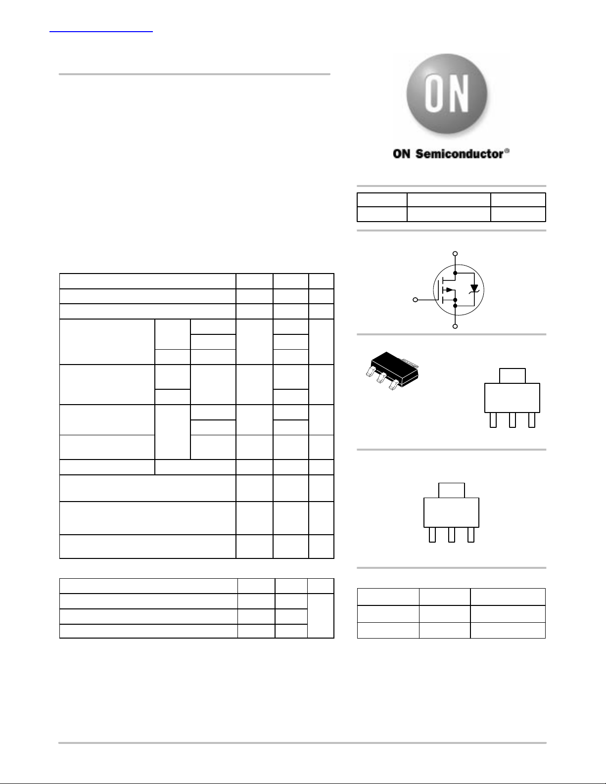
P−Channel
D
G
S
ID MAXV
−2.6 A
MARKING
4
1
2
3
2955 = Device Code
L = Location Code
WW = Work Week
SOT−223
CASE 318E
STYLE 3
DIAGRAM
2955
LWW
PIN ASSIGNMENT
4
Drain
Gate Drain Source
321
ORDERING INFORMATION
Device Package Shipping
NTF2955T1 SOT−223 1000/Tape & Reel
NTF2955T3 SOT−223 4000/Tape & Reel
†For information on tape and reel specifications,
including part orientation and tape sizes, please
refer to our Tape and Reel Packaging Specification
Brochure, BRD8011/D.
†
Semiconductor Components Industries, LLC, 2004
August, 2004 − Rev. 1
1 Publication Order Number:
NTF2955/D
NTF2955
()
R
L
25 Ω
V
GS
= 0 V, dIS/dt = 100 A/s
ELECTRICAL CHARACTERISTICS (T
Parameter
=25°C unless otherwise stated)
J
Symbol Test Condition Min Typ Max Unit
OFF CHARACTERISTICS
Drain−to−Source Breakdown Voltage
Drain−to−Source Breakdown Voltage
Temperature Coefficient
V
V
(BR)DSS/TJ
Zero Gate Voltage Drain Current I
Gate−to−Source Leakage Current I
(BR)DSS
DSS
GSS
V
V
V
DS
V
GS
GS
DS
= 0 V,
= −60 V
= 0 V, I
= 0 V, V
= −250 A −60 V
D
T
T
= ±20 V ±100 nA
GS
ON CHARACTERISTICS (Note 3)
Gate Threshold Voltage
V
Drain−to−Source On Resistance R
Forward Transconductance g
GS(TH)
DS(on)
FS
V
= VDS, ID = −1.0 mA −2.0 −4.0 V
GS
V
= −10 V, I
GS
V
= −10 V, I
GS
VGS = −10 V, I
V
= −15 V, I
GS
= −0.75 A 145 170
D
= −1.5 A 150 180
D
= −2.4 A 154 185
D
= −0.75 A 1.77 S
D
CHARGES AND CAPACITANCES
V
Input Capacitance
Output Capacitance C
Reverse Transfer Capacitance C
Total Gate Charge Q
Threshold Gate Charge Q
Gate−to−Source Charge Q
Gate−to−Drain Charge Q
C
ISS
OSS
RSS
G(TOT)
G(TH)
GS
GD
= 0 V, f = 1.0 MHz,
GS
V
GS
V
DS
= 10 V, V
I
= 1.5 A
D
= 25 V
DS
= 30 V,
SWITCHING CHARACTERISTICS (Note 4)
Turn−On Delay Time
t
d(ON)
Rise Time t
Turn−Off Delay Time t
d(OFF)
Fall Time t
V
= 10 V, V
GS
I
= 1.5 A, R
r
f
D
R
= 25 Ω
L
= 25 V,
DD
= 9.1 Ω
G
DRAIN−SOURCE DIODE CHARACTERISTICS
Forward Diode Voltage
Reverse Recovery Time t
Charge Time t
Discharge Time t
Reverse Recovery Charge Q
V
SD
RR
a
b
RR
V
V
= 0 V,
GS
I
= 1.5 A
S
= 0 V, dI
/dt = 100 A/s,
I
= 1.5 A
S
T
T
3. Pulse Test: pulse width ≤ 300s, duty cycle ≤ 2%.
4. Switching characteristics are independent of operating junction temperatures.
66.4 mV/°C
= 25°C −1.0
J
= 125°C −50
J
492
165
50
14.3
1.2
2.3
5.2
11
7.6
65
38
= 25°C −1.10 −1.30
J
= 125°C −0.9
J
36
,
20
16
0.139 nC
A
mΩ
pF
nC
ns
V
ns
http://onsemi.com
2

NTF2955
TYPICAL PERFORMANCE CURVES (T
10
8
6
4
DRAIN CURRENT (AMPS)
2
D,
−I
0
0
−V
DRAIN−TO−SOURCE VOLTAGE (VOLTS)
DS,
Figure 1. On−Region Characteristics Figure 2. Transfer Characteristics
0.4
VGS = −10 V
0.3
0.2
0.1
VGS = −10 V to −7 V
3
VGS = −6 V
TJ = 25 °C
VGS = −5.5 V
VGS = −5 V
VGS = −4.5 V
VGS = −3.8 V
456789
TJ = 125°C
TJ = 25°C
TJ = −55°C
= 25°C unless otherwise noted)
J
10
V
≥ 10 V
DS
8
TJ = 25°C
TJ = −55°C
TJ = 125°C
6
4
DRAIN CURRENT (AMPS)
2
D,
−I
1021
0
210846
−V
GATE−TO−SOURCE VOLTAGE (VOLTS)
GS,
0.25
0.225
TJ = 25°C
0.2
0.175
VGS = −10 V
0.15
0.125
VGS = −15 V
0.1
DRAIN−TO−SOURCE RESISTANCE (Ω)
0
DS(on),
R
0
−I
44
DRAIN CURRENT (AMPS)
D,
Figure 3. On−Resistance versus Drain Current
and Temperature
2
ID = −1.5 A
1.8
V
= −10 V
GS
1.6
1.4
1.2
1
0.8
0.6
0.4
0.2
0
−50 50250−25 75 125100
DRAIN−TO−SOURCE RESISTANCE (NORMALIZED)
DS(on),
R
T
, JUNCTION TEMPERATURE (°C)
J
Figure 5. On−Resistance Variation with
Temperature
0.075
DRAIN−TO−SOURCE RESISTANCE (Ω)
0.05
82
106
DS(on),
R
0
2
1086
−ID, DRAIN CURRENT (AMPS)
Figure 4. On−Resistance versus Drain Current
and Gate Voltage
1000
VGS = 0 V
TJ = 150°C
100
, LEAKAGE (nA)
−I
150
DSS
10
54060302010 50
−V
DRAIN−TO−SOURCE VOLTAGE (VOLTS)
DS,
TJ = 125°C
45352515 55
Figure 6. Drain−to−Source Leakage Current
versus V oltage
http://onsemi.com
3

NTF2955
TYPICAL PERFORMANCE CURVES (T
1200
1000
VDS = 0 V
C
iss
VGS = 0 V
800
C
rss
600
400
C, CAPACITANCE (pF)
200
0
10 10 155020525
−V
−V
GS
DS
GATE−TO−SOURCE OR DRAIN−T O−SOURCE VOLTAGE (VOLTS)
Figure 7. Capacitance Variation
1000
VDD = −25 V
I
= −1.5 A
D
V
= −10 V
GS
TJ = 25°C
C
C
C
iss
oss
rss
= 25°C unless otherwise noted)
J
12
Q
10
T
8
Q
GS
Q
GD
6
4
V
DS
2
, GATE−TO−SOURCE VOLTAGE (VOLTS)
0
GS
0108416
V
Q
62
, TOTAL GATE CHARGE (nC)
g
Figure 8. Gate−to−Source and
Drain−to−Source Voltage versus T otal Charge
5
VGS = 0 V
T
= 25°C
J
4
V
GS
ID = −1.5 A
T
= 25°C
J
1412
60
50
40
30
20
10
0
V
DS
, DRAIN−TO−SOURCE VOLTAGE (VOLTS)
100
t
d(off)
t
f
t, TIME (ns)
10
1
t
d(on)
t
r
1 10 100 0 0.50.25
3
2
1
, SOURCE CURRENT (AMPS)
S
−I
0
RG, GATE RESISTANCE (Ω)
Figure 9. Resistive Switching Time Variation
Figure 10. Diode Forward Voltage versus Current
versus Gate Resistance
100
VGS = −20 V
SINGLE PULSE
= 25°C
10
T
C
10 µs
100 µs
1 ms
1
10 ms
dc
0.1
, DRAIN CURRENT (AMPS)
D
−I
THERMAL LIMIT
R
DS(on)
LIMIT
PACKAGE LIMIT
0.01
0.1 10 1001 25 125 15010075 17550
−VDS, DRAIN−TO−SOURCE VOLTAGE (VOLTS)
250
200
150
100
50
AVALANCHE ENERGY (mJ)
, SINGLE PULSE DRAIN−TO−SOURCE
0
AS
E
Figure 11. Maximum Rated Forward Biased
Safe Operating Area
0.75 1
1.25 1.5
−VSD, SOURCE−TO−DRAIN VOLTAGE (VOLTS)
IPK = −6.7 A
TJ, STARTING JUNCTION TEMPERATURE (°C)
Figure 12. Maximum Avalanche Energy versus
Starting Junction Temperature
1.75
http://onsemi.com
4

0.08 (0003)
S
L
H
A
F
4
123
G
NTF2955
PACKAGE DIMENSIONS
SOT−223 (TO−261)
CASE 318E−04
ISSUE K
B
D
C
M
K
NOTES:
1. DIMENSIONING AND TOLERANCING PER ANSI
Y14.5M, 1982.
2. CONTROLLING DIMENSION: INCH.
INCHES
DIMAMIN MAX MIN MAX
0.249 0.263 6.30 6.70
B 0.130 0.145 3.30 3.70
C 0.060 0.068 1.50 1.75
D 0.024 0.035 0.60 0.89
F 0.115 0.126 2.90 3.20
G 0.087 0.094 2.20 2.40
H 0.0008 0.0040 0.020 0.100
J 0.009 0.014 0.24 0.35
K 0.060 0.078 1.50 2.00
L 0.033 0.041 0.85 1.05
M 0 10 0 10
J
S 0.264 0.287 6.70 7.30
STYLE 3:
PIN 1. GATE
2. DRAIN
3. SOURCE
4. DRAIN
MILLIMETERS
2.0
0.079
SOLDERING FOOTPRINT
3.8
0.15
2.0
0.079
2.3
0.091
1.5
0.059
2.3
0.091
6.3
0.248
http://onsemi.com
5

NTF2955
ON Semiconductor and are registered trademarks of Semiconductor Components Industries, LLC (SCILLC). SCILLC reserves the right to make changes without further notice
to any products herein. SCILLC makes no warranty, representation or guarantee regarding the suitability of its products for any particular purpose, nor does SCILLC assume any liability
arising out of the application or use of any product or circuit, and specifically disclaims any and all liability, including without limitation special, consequential or incidental damages.
“Typical” parameters which may be provided in SCILLC data sheets and/or specifications can and do vary in different applications and actual performance may vary over time. All
operating parameters, including “Typicals” must be validated for each customer application by customer’s technical experts. SCILLC does not convey any license under its patent rights
nor the rights of others. SCILLC products are not designed, intended, or authorized for use as components in systems intended for surgical implant into the body, or other applications
intended to support or sustain life, or for any other application in which the failure of the SCILLC product could create a situation where personal injury or death may occur. Should
Buyer purchase or use SCILLC products for any such unintended or unauthorized application, Buyer shall indemnify and hold SCILLC and its officers, employees, subsidiaries, affiliates,
and distributors harmless against all claims, costs, damages, and expenses, and reasonable attorney fees arising out of, directly or indirectly, any claim of personal injury or death
associated with such unintended or unauthorized use, even if such claim alleges that SCILLC was negligent regarding the design or manufacture of the part. SCILLC is an Equal
Opportunity/Affirmative Action Employer. This literature is subject to all applicable copyright laws and is not for resale in any manner.
PUBLICATION ORDERING INFORMATION
LITERATURE FULFILLMENT:
Literature Distribution Center for ON Semiconductor
P.O. Box 61312, Phoenix, Arizona 85082−1312 USA
Phone: 480−829−7710 or 800−344−3860 Toll Free USA/Canada
Fax: 480−829−7709 or 800−344−3867 Toll Free USA/Canada
Email: orderlit@onsemi.com
N. American Technical Support: 800−282−9855 Toll Free
USA/Canada
Japan: ON Semiconductor, Japan Customer Focus Center
2−9−1 Kamimeguro, Meguro−ku, Tokyo, Japan 153−0051
Phone: 81−3−5773−3850
http://onsemi.com
ON Semiconductor Website: http://onsemi.com
Order Literature: http://www.onsemi.com/litorder
For additional information, please contact your
local Sales Representative.
NTF2955/D
6
 Loading...