

NTD78N03
y
)
e
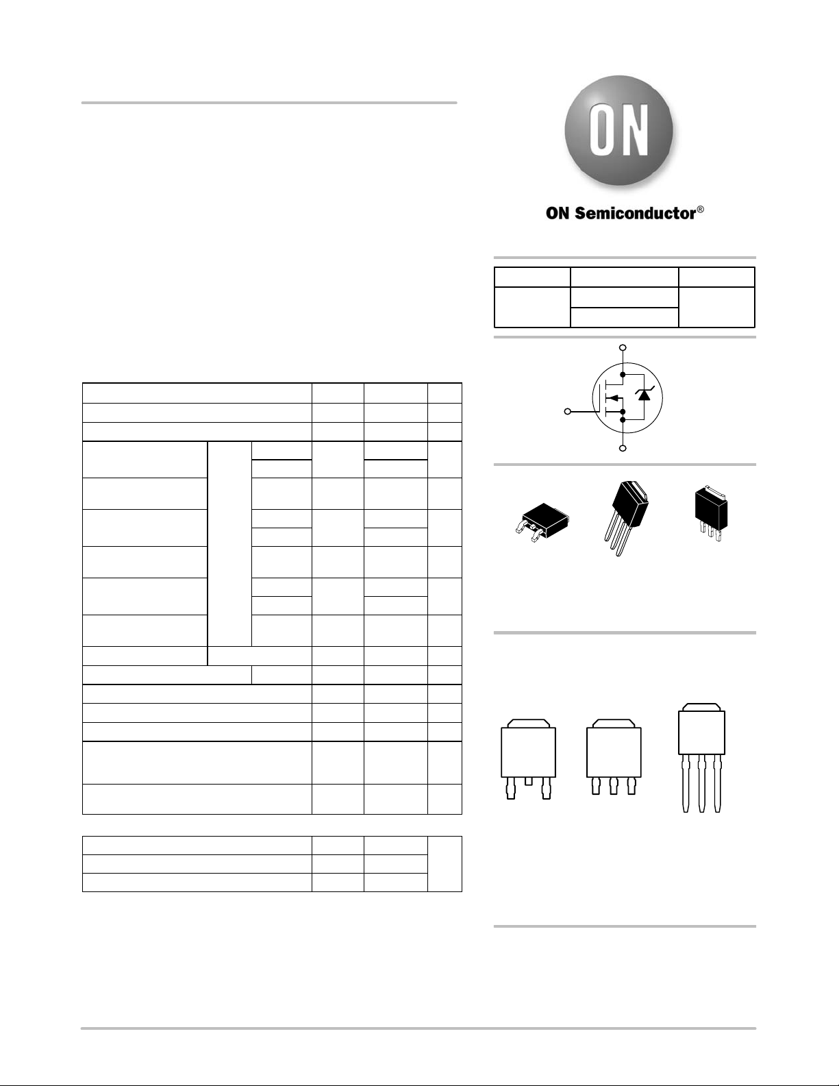
Power MOSFET
25 V, 78 A, Single N−Channel, DPAK
Features
• Low R
• Optimized Gate Charge
• Pb−Free Packages are Available
Applications
• Desktop VCORE
• DC−DC Converters
• Low Side Switch
MAXIMUM RATINGS (T
Drain−to−Source Voltage V
Gate−to−Source Voltage V
Continuous Drain
Current (Note 1)
Power Dissipation
(Note 1)
Continuous Drain
Current (Note 2)
Power Dissipation
(Note 2)
Continuous Drain
Current (R
Power Dissipation
(R
Pulsed Drain Current
Current Limited by Package TA = 25°C I
Drain to Source dV/dt dV/dt 8.0 V/ns
Operating Junction and Storage Temperature TJ, T
Source Current (Body Diode) I
Single Pulse Drain−to−Source Avalanche
Energy (VDD = 24 V, VGS = 10 V,
L = 5.0 mH, IL(pk) = 17 A, RG = 25 W)
Lead Temperature for Soldering Purposes
(1/8″ from case for 10 seconds)
THERMAL RESISTANCE
Junction−to−Case (Drain)
Junction−to−Ambient − Steady State (Note 1)
Junction−to−Ambient − Steady State (Note 2)
Stresses exceeding Maximum Ratings may damage the device. Maximum
Ratings are stress ratings only. Functional operation above the Recommended
Operating Conditions is not implied. Extended exposure to stresses above the
Recommended Operating Conditions may affect device reliability.
1. Surface−mounted on FR4 board using 1 in sq pad size (Cu area = 1.127 in
2. Surface−mounted on FR4 board using the minimum recommended pad size.
DS(on)
J
Parameter Symbol Value Unit
Stead
)
q
JC
)
q
JC
sq [1 oz] including traces).
= 25°C unless otherwise noted)
DSS
GS
TC = 25°C
TC = 85°C 11.5
TC = 25°C P
TC = 25°C
TC = 85°C 8.8
State
TC = 25°C P
TC = 25°C
TC = 85°C 56
TC = 25°C P
tp = 10 ms
I
D
D
I
D
D
I
D
D
I
DM
DmaxPkg
stg
S
E
AS
T
L
R
q
JC
R
q
JA
R
q
JA
25 V
"20 V
14.8
2.3 W
11.4
1.4 W
78
64 W
210 A
45 A
−55 to 175 °C
78 A
722.5 mJ
260 °C
1.95
65
110
°C/W
http://onsemi.com
R
TYP
(BR)DSS
25 V
G
A
A
2
1
3
A
CASE 369AA
DPAK
(Bend Lead)
STYLE 2
DS(on)
4.6 @ 10 V
6.5 @ 4.5 V
D
4
1
2
CASE 369D
DPAK
(Straight Lead)
STYLE 2
S
4
3
ID MAXV
78 A
N−Channel
4
1
2
3
CASE 369AD
IPAK
(Straight Lead
MARKING DIAGRAMS
& PIN ASSIGNMENTS
4
Gate
1
Drain
YWW78N03G
2
3
Drain
Sourc
Drain
YWW78N03G
Drain
1
Gate
4
2
3
Source
Y = Year
WW = Work Week
78N03 = Device Code
G = Pb−Free Package
Gate
1
4
Drain
YWW78N03G
2
Drain
3
Source
ORDERING INFORMATION
See detailed ordering and shipping information in the package
dimensions section on page 5 of this data sheet.
© Semiconductor Components Industries, LLC, 2006
September, 2006 − Rev. 6
1 Publication Order Number:
NTD78N03/D
NTD78N03
ELECTRICAL CHARACTERISTICS (T
= 25°C unless otherwise noted)
J
Parameter Symbol Test Condition Min Typ Max Unit
OFF CHARACTERISTICS
Drain−to−Source Breakdown Voltage V
Drain−to−Source Breakdown Voltage
Temperature Coefficient
V
(BR)DSS/TJ
Zero Gate Voltage Drain Current I
Gate−to−Source Leakage Current I
(BR)DSS
DSS
GSS
VGS = 0 V, ID = 250 mA
VGS = 0 V,
VDS = 20 V
TJ = 25°C 1.5 mA
TJ = 125°C 10
VDS = 0 V, VGS = "20 V "100 nA
25 V
24 mV/°C
ON CHARACTERISTICS (Note 3)
Gate Threshold Voltage V
Negative Threshold Temperature Coefficient V
Drain−to−Source On Resistance R
GS(TH)
GS(TH)/TJ
DS(on)
VGS = VDS, ID = 250 mA
VGS = 10 V, ID = 78 A 4.6 6.0 mW
1.0 1.6 3.0 V
−5.0 mV/°C
VGS = 4.5 V, ID = 36 A 6.5 7.8
Forward Transconductance gFS VDS = 10 V, ID = 15 A 22 S
CHARGES, CAPACITANCES AND GATE RESISTANCE
Input Capacitance C
Output Capacitance C
Reverse Transfer Capacitance C
Total Gate Charge Q
Threshold Gate Charge Q
Gate−to−Source Charge Q
Gate−to−Drain Charge Q
iss
oss
rss
G(TOT)
G(TH)
GS
GD
VGS = 0 V, f = 1.0 MHz,
VDS = 12 V
VGS = 4.5 V, VDS = 20 V,
ID = 20 A
1920 2250
960
420
25.5 35
2.4
5.3
18.2
SWITCHING CHARACTERISTICS (Note 4)
Turn−On Delay Time t
Rise Time t
Turn−Off Delay Time t
Fall Time t
d(on)
r
d(off)
f
VGS = 4.5 V, VDS = 20 V,
ID = 20 A, R
= 3.0 W
G
11
68
23
42
DRAIN−SOURCE DIODE CHARACTERISTICS
Forward Diode Voltage V
SD
VGS = 0 V,
IS = 20 A
Reverse Recovery Time t
Charge Time ta 17.8
Discharge Time tb 21
Reverse Recovery Time Q
RR
VGS = 0 V, dIs/dt = 100 A/ms,
IS = 20 A
RR
TJ = 25°C 0.83 1.0
TJ = 125°C 0.7
39
33 nC
PACKAGE PARASITIC VALUES
Source Inductance L
Drain Inductance L
Gate Inductance L
Gate Resistance R
S
D
G
G
Ta = 25C
2.49
0.02
3.46
1.0
3. Pulse Test: Pulse Width ≤ 300 ms, Duty Cycle ≤ 2%.
4. Switching characteristics are independent of operating junction temperatures.
pF
nC
ns
V
ns
nH
W
http://onsemi.com
2
NTD78N03
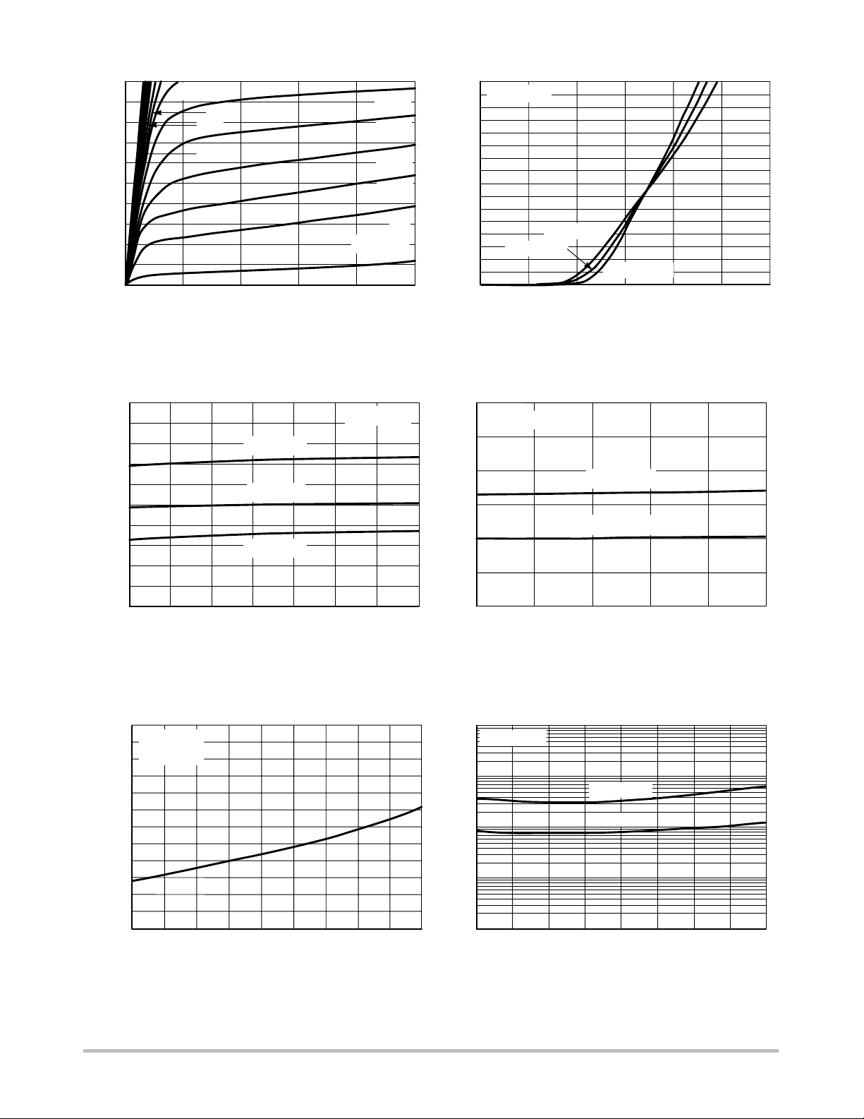
R
, DRAIN−TO−SOURCE RESISTANCE (
)
6
R
, DRAIN−TO−SOURCE RESISTANCE
100
VGS = 4 V
4.5 V
5 V
9 V
TJ = 25°C
2
VDS, DRAIN−TO−SOURCE VOLTAGE (V)
864
3.8 V
3.6 V
3.4 V
3.2 V
3 V
2.6 V
10
90
80
70
60
50
40
30
20
, DRAIN CURRENT (AMPS)
D
I
10
0
0
Figure 1. On−Region Characteristics
W
0.01
0.009
0.008
0.007
0.006
0.005
0.004
0.003
0.002
0.001
DS(on)
0
10
20 60 70 80
TJ = 125°C
TJ = 25°C
TJ = −55°C
40
5030
ID, DRAIN CURRENT (A)
VGS = 10 V
160
VDS ≥ 10 V
150
140
130
120
110
100
90
80
70
60
50
40
, DRAIN CURRENT (AMPS)
30
D
I
20
10
0
03
TJ = 125°C
TJ = 25°C
TJ = −55°C
21
VGS, GATE−TO−SOURCE VOLTAGE (V)
45
Figure 2. Transfer Characteristics
0.015
TJ = 25°C
0.01
0.005
, DRAIN−TO−SOURCE RESISTANCE (W)
DS(on)
R
0
55
60 65 70 75 80
VGS = 4.5 V
VGS = 10 V
ID, DRAIN CURRENT (A)
Figure 3. On−Resistance versus
Drain Current and Temperature
3
ID = 78 A
V
= 4.5 V
DS
2.5
2
1.5
1
(NORMALIZED)
0.5
0
DS(on)
−50 100750−25 125 175
TJ, JUNCTION TEMPERATURE (°C)
5025
Figure 5. On−Resistance Variation with
Temperature
100000
10000
1000
, LEAKAGE (nA)
DSS
I
100
10
150
5201510 25
http://onsemi.com
3
Figure 4. On−Resistance versus Drain Current
and Gate Voltage
VGS = 0 V
TJ = 150°C
TJ = 125°C
VDS, DRAIN−TO−SOURCE VOLTAGE (V)
Figure 6. Drain−To−Source Leakage
Current versus Voltage
 Loading...