

查询NTB65N02R供应商
NTB65N02R, NTP65N02R
Product Preview
Power MOSFET
65 A, 24 V N-Channel
2
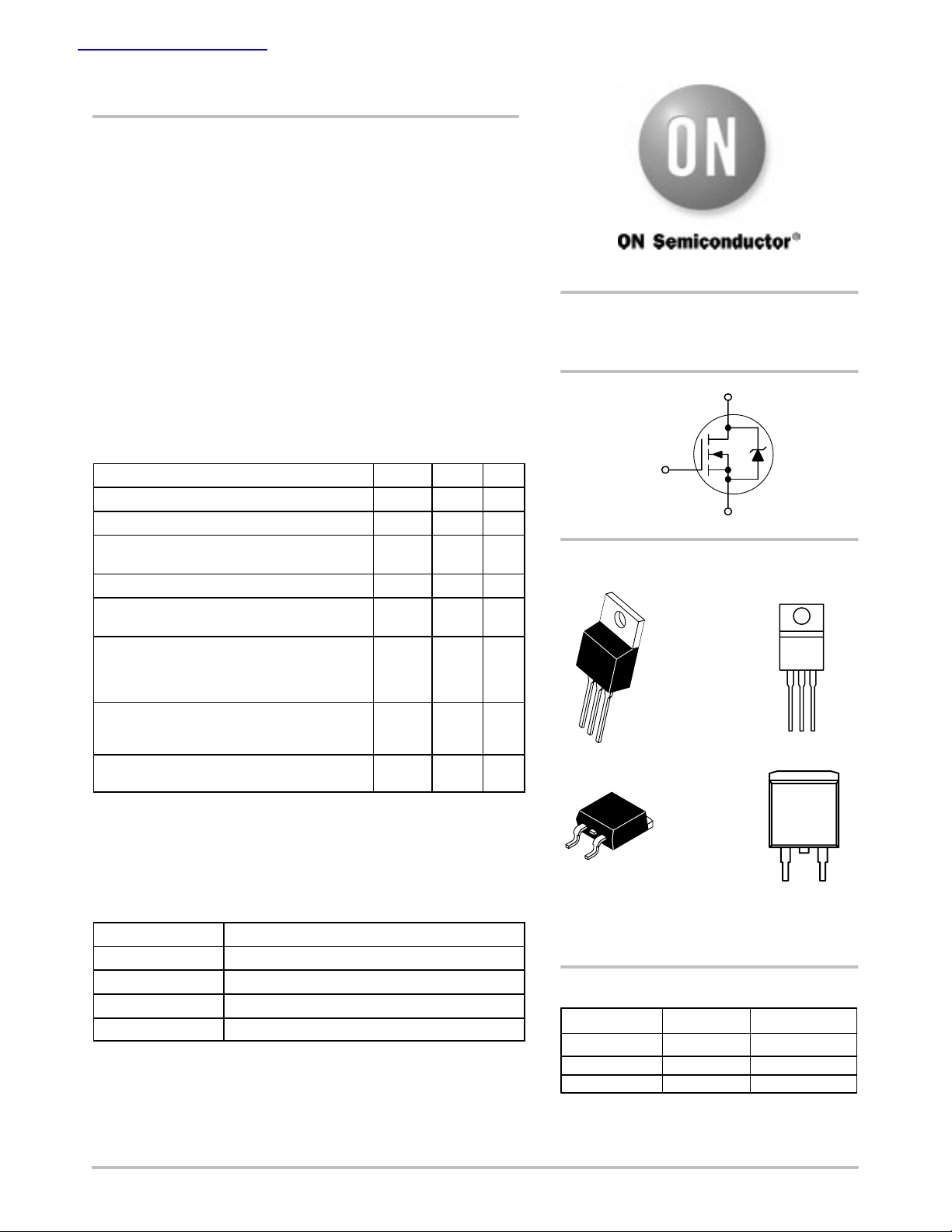
TO-220, D
Features
• Planar HD3e Process for Fast Switching Performance
• Low R
• Low C
• Low Gate Charge
• Fast Switching
to Minimize Conduction Loss
DSon
to Minimize Driver Loss
iss
PAK
http://onsemi.com
65 A, 24 V
R
DS(on)
= 8.3 m (TYP)
D
MAXIMUM RATINGS (T
Parameter
Drain–to–Source Voltage V
Gate–to–Source Voltage Continuous V
Drain Current(Continuous @ TA = 25°C (Note 3)
Total Power Dissipation @ TA = 25°C P
Operating and Storage Temperature TJ and
Single Pulse Drain–to Source Avalanche
Energy – Starting T
= 50 Vdc, V
(V
DD
R
= 25 )
G
Thermal Resistance Junction–to–Case
Maximum Lead Temperature for Soldering
Purposes, 1/8” from Case for 10 Seconds
1. When surface mounted to an FR4 board using 1 inch pad size, (Cu Area
1.127 in
2. When surface mounted to an FR4 board using minimum recommended pad
size, (Cu Area 0.412 in
3. Chip current capability limited by package.
J
GS
Junction–to–Ambient (Note 1)
Junction–to–Ambient (Note 2)
2
).
= 25°C Unless otherwise specified)
J
Single Pulse (tp = 10 s)
=25°C
= 5 Vdc, IL = Apk, L = 1 mH,
2
).
Symbol Value Unit
24 V
±20 V
65
160
78 W
–55 to
150
TBD mJ
1.6
°C/W
67
120
260 °C
dc
dc
A
A
°C
R
R
R
I
T
E
DSS
GS
I
D
DM
D
stg
AS
JC
JA
JA
T
L
G
S
MARKING
DIAGRAMS
TO–220AB
4
CASE 221A
Style 5
1
2
3
2
PAK
D
4
CASE 418B
2
1
3
Style 2
xxxxx
YWW
xxxxx
YWW
PIN ASSIGNMENT
PIN FUNCTION
1 Gate
2 Drain
3 Source
4 Drain
This document contains information on a product under development. ON Semiconductor
reserves the right to change or discontinue this product without notice.
Semiconductor Components Industries, LLC, 2002
October, 2002 – Rev. 0
1 Publication Order Number:
xxxxx = Specific Device Code
Y = Year
WW = Work Week
ORDERING INFORMATION
Device Package Shipping
NTB65N02R D
NTB65N02RT4 D2PAK 800 Tape & Reel
NTP65N02R TO–220AB 50 Units/Rail
2
PAK
50 Units/Rail
NTB65N02R/D
NTB65N02R, NTP65N02R
(
DS dc,GS
)
(V
GS
V
d
V
DD
V
d
)
V
DS
V
d
) (Note 4)
g
Forward On Voltage
(I
S
A
d
V
GS
V
d
) (Note 4)
V
SD
0.88
1.2–V
d
(
S dc,GS dc
)
(I
S
A
d
V
GS
V
d
ELECTRICAL CHARACTERISTICS (T
Characteristics
= 25°C Unless otherwise specified)
J
Symbol Min Typ Max Unit
OFF CHARACTERISTICS
Drain–to–Source Breakdown Voltage (Note 4)
(V
= 0 Vdc, I
GS
Temperature Coefficient (Positive)
= 250 Adc)
D
Zero Gate Voltage Drain Current
(V
= 20 Vdc, VGS = 0 Vdc)
DS
= 20 Vdc, VGS = 0 Vdc, TJ = 150°C)
(V
DS
Gate–Body Leakage Current
(VGS = ±20 Vdc, VDS = 0 Vdc)
V(br)
I
DSS
I
GSS
DSS
24
–
–
–
27.5
25.5
–
–
– – ±100
ON CHARACTERISTICS (Note 4)
Gate Threshold Voltage (Note 4)
(VDS = VGS, ID = 250 Adc)
Threshold Temperature Coefficient (Negative)
Static Drain–to–Source On–Resistance (Note 4)
(VGS = 4.5 Vdc, ID = 15 Adc)
(V
= 10 Vdc, ID = 20 Adc)
GS
(V
= 10 Vdc, ID = 30 Adc)
GS
Forward Transconductance (Note 4)
(VDS = 10 Vdc, ID = 15 Adc)
VGS(th)
RDS(on)
g
FS
1.0
–
–
–
–
1.5
–4.1
10.5
8.3
9.5
– 20 –
12.5
10.5
DYNAMIC CHARACTERISTICS
Input Capacitance
Output Capacitance
Transfer Capacitance
(VDS = 24 Vdc, VGS = 0 V f = 1 MHz)
C
iss
C
oss
C
rss
– 1050 1470
– 394 550
– 88 120
SWITCHING CHARACTERISTICS (Note 5)
Turn–On Delay Time
Rise Time
Turn–Off Delay Time
(V
= 5 V
, VDD = 10 V
= 5
,
ID = 30 Adc, RG = 3)
c
= 10
,
,
c
td(on) – 11.2 20
t
r
– 52 100
td(off) – 10 20
Fall Time tf – 4 10
Gate Charge
(VGS = 4.5 Vdc, ID = 30 Adc,
V
= 10 V) (Note 4
= 10
c
Q
T
Q
1
Q
2
– 8.4 12
– 3.7 –
– 4.04 –
SOURCE–DRAIN DIODE CHARACTERISTICS
Forward On–Volta
e (I
= 20 A
= 20
, V
= 0 V
,
= 0
c
(IS = 30 Adc, VGS = 0 Vdc)
c
) (Note 4) V
D
– 0.88 1.2 V
–
1.10
(IS = 20 Adc, VGS = 0 Vdc, TJ = 125°C) – 0.80 –
Reverse Recovery Time
(I
= 20 A
= 20
dIS/dt = 100 A/s) (Note 4)
, V
= 0 V
= 0
,
,
c
,
c
Reverse Recovery Stored Charge Q
t
t
t
rr
a
b
RR
– 15.5 –
– 12.6 –
– 2.6 –
– 0.005 – C
4. Pulse Test: Pulse Width = 300 s, Duty Cycle = 2%.
5. Switching characteristics are independent of operating junction temperatures.
1.5
15
2.0
V
–
–
–
dc
mV/°C
A
dc
nA
dc
V
dc
mV/°C
m
–
Mhos
pF
ns
nC
c
ns
http://onsemi.com
2

NTB65N02R, NTP65N02R
PACKAGE DIMENSIONS
TO–220AB
CASE 221A–09
ISSUE AA
SEATING
–T–
PLANE
B
4
Q
123
F
T
A
U
C
S
H
K
Z
L
V
R
J
G
D
N
NOTES:
1. DIMENSIONING AND TOLERANCING PER ANSI
Y14.5M, 1982.
2. CONTROLLING DIMENSION: INCH.
3. DIMENSION Z DEFINES A ZONE WHERE ALL
BODY AND LEAD IRREGULARITIES ARE
ALLOWED.
DIM MIN MAX MIN MAX
A 0.570 0.620 14.48 15.75
B 0.380 0.405 9.66 10.28
C 0.160 0.190 4.07 4.82
D 0.025 0.035 0.64 0.88
F 0.142 0.147 3.61 3.73
G 0.095 0.105 2.42 2.66
H 0.110 0.155 2.80 3.93
J 0.018 0.025 0.46 0.64
K 0.500 0.562 12.70 14.27
L 0.045 0.060 1.15 1.52
N 0.190 0.210 4.83 5.33
Q 0.100 0.120 2.54 3.04
R 0.080 0.110 2.04 2.79
S 0.045 0.055 1.15 1.39
T 0.235 0.255 5.97 6.47
U 0.000 0.050 0.00 1.27
V 0.045 --- 1.15 ---
Z --- 0.080 --- 2.04
STYLE 5:
PIN 1. GATE
2. DRAIN
3. SOURCE
4. DRAIN
MILLIMETERSINCHES
–T–
SEATING
PLANE
–B–
G
D2PAK
CASE 418B–04
ISSUE G
NOTES:
C
E
V
4
W
A
231
S
K
W
J
3 PL
D
0.13 (0.005) T
M
M
B
H
1. DIMENSIONING AND TOLERANCING PER ANSI
Y14.5M, 1982.
2. CONTROLLING DIMENSION: INCH.
3. 418B-01 THRU 418B-03 OBSOLETE, NEW
STANDARD 418B-04.
DIM MIN MAX MIN MAX
A 0.340 0.380 8.64 9.65
B 0.380 0.405 9.65 10.29
C 0.160 0.190 4.06 4.83
D 0.020 0.035 0.51 0.89
E 0.045 0.055 1.14 1.40
F 0.310 0.350 7.87 8.89
G 0.100 BSC 2.54 BSC
H 0.080 0.110 2.03 2.79
J 0.018 0.025 0.46 0.64
K 0.090 0.110 2.29 2.79
L 0.052 0.072 1.32 1.83
M 0.280 0.320 7.11 8.13
N 0.197 REF 5.00 REF
P 0.079 REF 2.00 REF
R 0.039 REF 0.99 REF
S 0.575 0.625 14.60 15.88
V 0.045 0.055 1.14 1.40
STYLE 2:
PIN 1. GATE
2. DRAIN
3. SOURCE
4. DRAIN
MILLIMETERSINCHES
http://onsemi.com
3

NTB65N02R, NTP65N02R
ON Semiconductor and are registered trademarks of Semiconductor Components Industries, LLC (SCILLC). SCILLC reserves the right to make
changes without further notice to any products herein. SCILLC makes no warranty, representation or guarantee regarding the suitability of its products for any
particular purpose, nor does SCILLC assume any liability arising out of the application or use of any product or circuit, and specifically disclaims any and all
liability, including without limitation special, consequential or incidental damages. “Typical” parameters which may be provided in SCILLC data sheets and/or
specifications can and do vary in different applications and actual performance may vary over time. All operating parameters, including “Typicals” must be
validated for each customer application by customer’s technical experts. SCILLC does not convey any license under its patent rights nor the rights of others.
SCILLC products are not designed, intended, or authorized for use as components in systems intended for surgical implant into the body, or other applications
intended to support or sustain life, or for any other application in which the failure of the SCILLC product could create a situation where personal injury or death
may occur. Should Buyer purchase or use SCILLC products for any such unintended or unauthorized application, Buyer shall indemnify and hold SCILLC
and its officers, employees, subsidiaries, affiliates, and distributors harmless against all claims, costs, damages, and expenses, and reasonable attorney fees
arising out of, directly or indirectly, any claim of personal injury or death associated with such unintended or unauthorized use, even if such claim alleges that
SCILLC was negligent regarding the design or manufacture of the part. SCILLC is an Equal Opportunity/Affirmative Action Employer.
PUBLICATION ORDERING INFORMATION
Literature Fulfillment:
Literature Distribution Center for ON Semiconductor
P.O. Box 5163, Denver, Colorado 80217 USA
Phone: 303–675–2175 or 800–344–3860 Toll Free USA/Canada
Fax: 303–675–2176 or 800–344–3867 Toll Free USA/Canada
Email: ONlit@hibbertco.com
N. American Technical Support: 800–282–9855 Toll Free USA/Canada
http://onsemi.com
JAPAN: ON Semiconductor, Japan Customer Focus Center
2–9–1 Kamimeguro, Meguro–ku, Tokyo, Japan 153–0051
Phone: 81–3–5773–3850
Email: r14525@onsemi.com
ON Semiconductor Website: http://onsemi.com
For additional information, please contact your local
Sales Representative.
NTB65N02R/D
4
 Loading...