

ON Semiconductor NTB30N20 User Manual
NTB30N20
l
l
Power MOSFET
30 Amps, 200 Volts
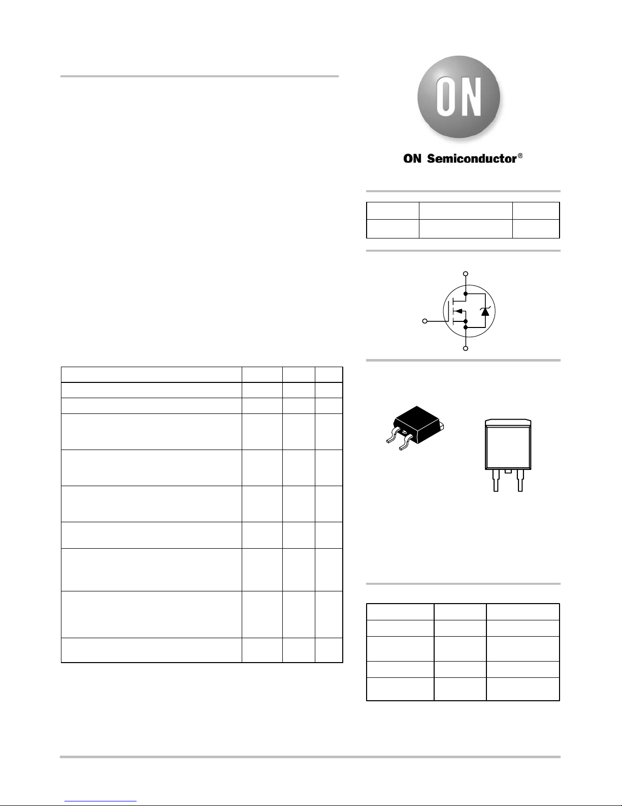
N−Channel Enhancement−Mode D2PAK
Features
• Source−to−Drain Diode Recovery Time Comparable to a Discrete
Fast Recovery Diode
• Avalanche Energy Specified
• I
and R
DSS
• Mounting Information Provided for the D
Specified at Elevated Temperature
DS(on)
2
PAK Package
• Pb−Free Packages are Available
Typical Applications
• PWM Motor Controls
• Power Supplies
• Converters
MAXIMUM RATINGS (T
Drain−to−Source Voltage V
Drain−to−Source Voltage (RGS = 1.0 MW)
Gate−to−Source Voltage
− Continuous
− Non−Repetitive (tpv10 ms)
Drain Current − Continuous @ TA 25°C
− Continuous @ TA 100°C
− Pulsed (Note 2)
Total Power Dissipation @ TA = 25°C
Derate above 25°C
Total Power Dissipation @ TA = 25°C (Note 1)
Operating and Storage Temperature Range TJ, T
Single Drain−to−Source Avalanche Energy,
Starting TJ = 25°C
(VDD = 100 Vdc, VGS = 10 Vdc,
IL(pk) = 20 A, L = 3.0 mH, RG = 25 W)
Thermal Resistance
− Junction−to−Case
− Junction−to−Ambient
− Junction−to−Ambient (Note 1)
Maximum Lead Temperature for Soldering
Purposes for 10 seconds
Maximum ratings are those values beyond which device damage can occur.
Maximum ratings applied to the device are individual stress limit values (not
normal operating conditions) and are not valid simultaneously. If these limits are
exceeded, device functional operation is not implied, damage may occur and
reliability may be affected.
1. When surface mounted to an FR4 board using the minimum recommended
pad size, (Cu Area 0.412 in2).
2. Pulse Test: Pulse Width = 10 ms, Duty Cycle = 2%.
= 25°C unless otherwise noted)
C
Rating Symbol Value Unit
D
D
stg
JC
JA
JA
L
200 Vdc
200 Vdc
"30
"40
30
22
90
214
1.43
2.0
− 55 to
+175
450
0.7
62.5
50
260 °C
Vdc
Adc
W
W/°C
W
°C
mJ
°C/W
DSS
V
DGR
V
GS
V
GSM
I
D
I
D
I
DM
P
P
E
AS
R
q
R
q
R
q
T
http://onsemi.com
V
DSS
200 V
R
TYP ID MAX
DS(ON)
68 mW @ VGS = 10 V
N−Channel
D
G
S
30 A
MARKING DIAGRAM
& PIN ASSIGNMENT
4
Gate
Drain
30N20G
AYWW
1
Drain
3
2
Source
4
1
2
3
D2PAK
CASE 418B
STYLE 2
30N20 = Device Code
A = Assembly Location
Y = Year
WW = Work Week
G = Pb−Free Package
ORDERING INFORMATION
Device Package Shipping
NTB30N20 D2PAK 50 Units/Rail
NTB30N20G D2PAK
(Pb−Free)
NTB30N20T4 D2PAK 800 Tape & Ree
NTB30N20T4G D2PAK
(Pb−Free)
†For information on tape and reel specifications,
including part orientation and tape sizes, please
refer to our Tape and Reel Packaging Specification
Brochure, BRD8011/D.
50 Units/Rail
800 Tape & Ree
†
© Semiconductor Components Industries, LLC, 2005
August, 2005 − Rev. 4
1 Publication Order Number:
NTB30N20/D
NTB30N20
ELECTRICAL CHARACTERISTICS (T
= 25°C unless otherwise noted)
C
Characteristic Symbol Min Typ Max Unit
OFF CHARACTERISTICS
Drain−to−Source Breakdown Voltage
(VGS = 0 Vdc, ID = 250 mAdc)
Temperature Coefficient (Positive)
Zero Gate Voltage Collector Current
(VGS = 0 Vdc, VDS = 200 Vdc, TJ = 25°C)
(VGS = 0 Vdc, VDS = 200 Vdc, TJ = 175°C)
Gate−Body Leakage Current (VGS = ± 30 Vdc, VDS = 0) I
ON CHARACTERISTICS
Gate Threshold Voltage
VDS = V
ID = 250 mAdc)
GS,
Temperature Coefficient (Negative)
Static Drain−to−Source On−State Resistance
(VGS = 10 Vdc, ID = 15 Adc)
(VGS = 10 Vdc, ID = 10 Adc)
(VGS = 10 Vdc, ID = 15 Adc, TJ = 175°C)
Drain−to−Source On−Voltage
(VGS = 10 Vdc, ID = 30 Adc)
Forward Transconductance (VDS = 15 Vdc, ID = 15 Adc) g
DYNAMIC CHARACTERISTICS
Input Capacitance (VDS = 25 Vdc, VGS = 0 Vdc, f = 1.0 MHz) C
Output Capacitance (VDS = 25 Vdc, VGS = 0 Vdc, f = 1.0 MHz)
(VDS = 160 Vdc, VGS = 0 Vdc, f = 1.0 MHz)
Reverse Transfer Capacitance (VDS = 25 Vdc, VGS = 0 Vdc, f = 1.0 MHz) C
SWITCHING CHARACTERISTICS (Notes 3 & 4)
Turn−On Delay Time
Rise Time t
(V
= 100 Vdc, ID = 18 Adc,
DD
VGS = 5.0 Vdc, RG = 2.5 W)
Turn−Off Delay Time t
(V
= 160 Vdc, ID = 30 Adc,
DD
VGS = 10 Vdc, RG = 9.1 W)
Fall Time t
Gate Charge
(VDS = 160 Vdc, ID = 30 Adc,
VGS = 10 Vdc)
(VDS = 160 Vdc, ID = 18 Adc,
VGS = 5.0 Vdc)
BODY−DRAIN DIODE RATINGS (Note 3)
Forward On−Voltage (IS = 30 Adc, VGS = 0 Vdc)
(IS = 30 Adc, VGS = 0 Vdc, TJ = 150°C)
Reverse Recovery Time
(IS = 30 Adc, VGS = 0 Vdc,
dIS/dt = 100 A/ms)
Reverse Recovery Stored Charge Q
3. Indicates Pulse Test: P. W. = 300 ms max, Duty Cycle = 2%.
4. Switching characteristics are independent of operating junction temperature.
V
(BR)DSS
I
DSS
GSS
V
GS(th)
R
DS(on)
V
DS(on)
C
t
d(on)
d(off)
Q
Q
Q
V
t
t
t
FS
iss
oss
rss
r
f
tot
gs
gd
SD
rr
a
b
RR
200
−
−
307
−
−
mV/°C
mAdc
Vdc
−
−
−
−
5.0
125
− − ± 100 nAdc
Vdc
2.0
−
−
−
−
2.9
−8.9
0.068
0.067
0.200
4.0
−
0.081
0.080
0.240
mV/°C
Vdc
− 2.0 2.5
− 20 − Mhos
− 2335 − pF
−
−
380
148
−
−
− 75 −
−
−
−
−
−
−
−
−
−
−
−
−
10
12
20
70
40
82
24
88
75
48
20
16
−
−
−
−
−
−
−
−
100
−
−
−
− 32 −
−
−
0.91
0.80
1.1
−
Vdc
− 230 −
− 140 −
− 85 −
− 1.85 −
W
ns
nC
ns
mC
http://onsemi.com
2
NTB30N20
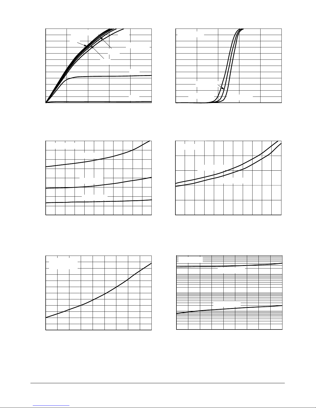
60
0
60
I
, DRAIN CURRENT (AMPS)
R
, DRAIN−TO−SOURCE RESISTANCE (
)
R
DRAIN−TO−SOURCE RESISTANCE (NORMALIZED)
0
50
40
30
D
W
0.15
20
10
0
0.2
0.1
VGS = 10 V
9 V
7 V
VDS, DRAIN−TO−SOURCE VOLTAGE (VOLTS)
6 V
TJ = 25°C
8 V
5 V
4 V
Figure 1. On−Region Characteristics
VGS = 10 V
TJ = 100°C
TJ = 25°C
VDS ≥ 10 V
50
40
30
20
, DRAIN CURRENT (AMPS)
D
10
I
106420
080
TJ = 25°C
TJ = 100°C
VGS, GATE−TO−SOURCE VOLTAGE (VOLTS)
TJ = −55°C
6420
1
Figure 2. Transfer Characteristics
0.1
TJ = 25°C
0.09
0.08
0.07
VGS = 10 V
VGS = 15 V
0.05
0
DS(on)
Figure 3. On−Resistance versus Drain Current
3
2.5
2
1.5
1
0.5
0
DS(on),
ID = 15 A
VGS = 10 V
TJ, JUNCTION TEMPERATURE (°C)
Figure 5. On−Resistance Variation with
TJ = −55°C
3525155
ID, DRAIN CURRENT (AMPS)
and Temperature
Temperature
0.06
, DRAIN−TO−SOURCE RESISTANCE (W)
5545
0.05
DS(on)
R
ID, DRAIN CURRENT (AMPS)
453525155
55
Figure 4. On−Resistance versus Drain Current
and Gate Voltage
100000
1751251007550250−25−50
10000
, LEAKAGE (nA)
DSS
I
1000
100
10
VGS = 0 V
TJ = 175°C
TJ = 100°C
4020
60 20
808100 120 140
VDS, DRAIN−TO−SOURCE VOLTAGE (VOLTS)
160 180150
Figure 6. Drain−to−Source Leakage Current
versus Voltage
http://onsemi.com
3
 Loading...