

NSTB1002DXV5T1G,
l
l
l
l
NSTB1002DXV5T5G
Preferred Devices
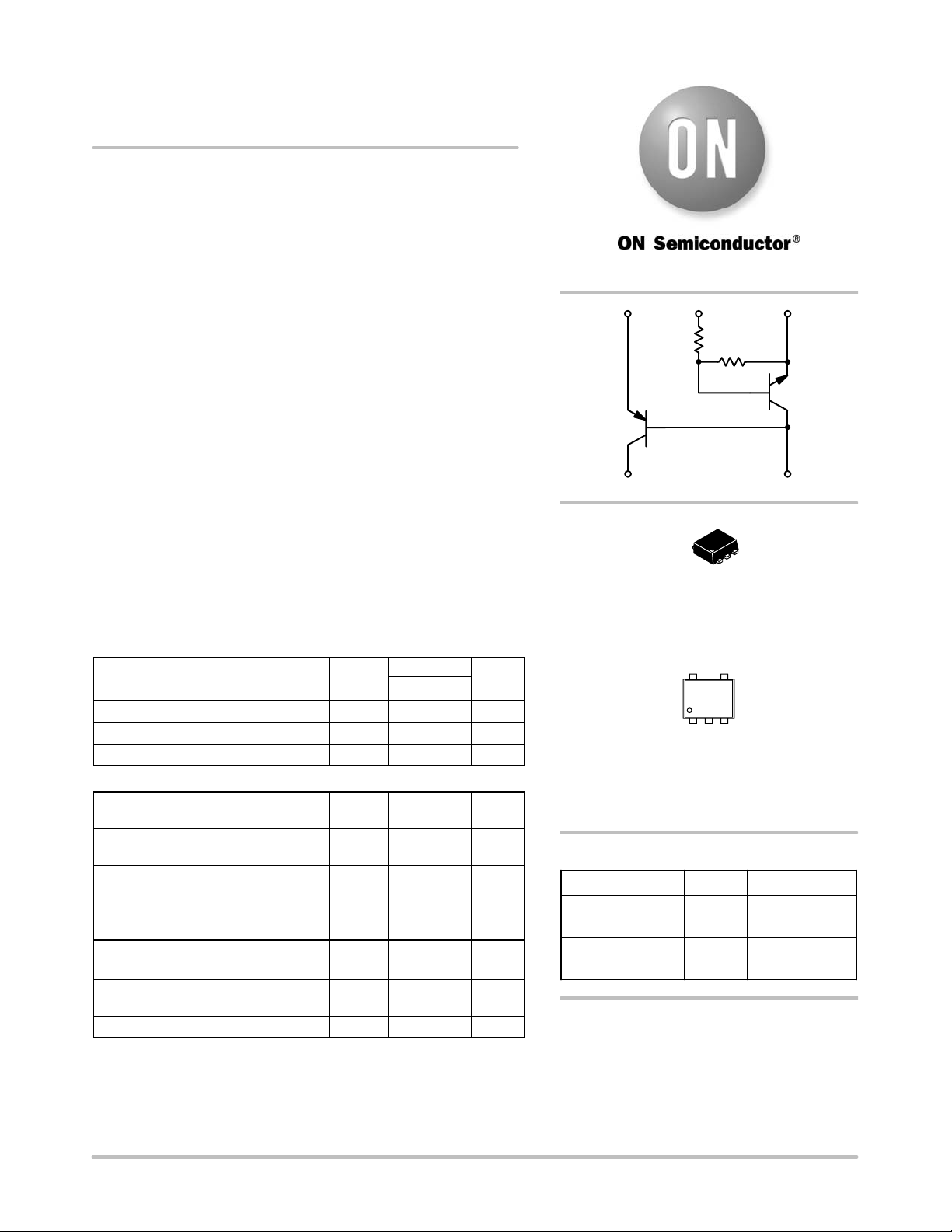
Dual Common
Base−Collector Bias
Resistor Transistors
NPN and PNP Silicon Surface Mount
Transistors with Monolithic Bias
Resistor Network
The BR T (Bias Resistor Transistor) contains a single transistor with
a monolithic bias network consisting of two resistors; a series base
resistor and a base−emitter resistor. These digital transistors are
designed to replace a single device and its external resistor bias
network. The BRT eliminates these individual components by
integrating them into a single device. In the NSTB1002DXV5T1G
series, two complementary devices are housed in the SOT−553
package which is ideal for low power surface mount applications
where board space is at a premium.
• Simplifies Circuit Design
• Reduces Board Space
• Reduces Component Count
• Available in 8 mm, 7 inch Tape and Reel
• These are Pb−Free Devices
MAXIMUM RATINGS (T
and Q2, − minus sign for Q1 (PNP) omitted)
Rating Symbo
Collector-Base Voltage V
Collector-Emitter Voltage V
Collector Current I
THERMAL CHARACTERISTICS
Characteristic
(One Junction Heated)
Total Device Dissipation TA = 25°C
Thermal Resistance −
Junction-to-Ambient
Characteristic
(Both Junctions Heated)
Total Device Dissipation TA = 25°C
Thermal Resistance −
Junction-to-Ambient
Junction and Storage Temperature TJ, T
Maximum ratings are those values beyond which device damage can occur.
Maximum ratings applied to the device are individual stress limit values (not
normal operating conditions) and are not valid simultaneously. If these limits are
exceeded, device functional operation is not implied, damage may occur and
reliability may be affected.
1. FR−4 @ Minimum Pad
= 25°C unless otherwise noted, common for Q
A
Value
Q1 Q2
CBO
CEO
Symbol Max Unit
P
Derate above 25°C
R
Symbo
P
Derate above 25°C
R
−40 50 Vdc
−40 50 Vdc
−200 100 mAdc
C
357 (Note 1)
D
2.9 (Note 1)mWmW/°C
350 (Note 1) °C/W
q
JA
Max Unit
500 (Note 1)
D
4.0 (Note 1)
250 (Note 1) °C/W
q
JA
− 55 to +150 °C
stg
1
Unit
mW
mW/°C
http://onsemi.com
312
R1
Q1
45
CASE 463B
R2
Q2
R1
5
1
SOT−553
MARKING DIAGRAM
5
U9 MG
G
1
U9 = Specific Device Code
M = Date Code
G = Pb−Free Package
(Note: Microdot may be in either location)
ORDERING INFORMATION
Device Package Shipping
NSTB1002DXV5T1G SOT−553
(Pb−Free)
NSTB1002DXV5T5G SOT−553
(Pb−Free)
Preferred devices are recommended choices for future use
and best overall value.
4 mm pitch
4000/Tape & Ree
2 mm pitch
8000/Tape & Ree
© Semiconductor Components Industries, LLC, 2006
January, 2006 − Rev. 0
1 Publication Order Number:
NSTB1002DXV5/D
NSTB1002DXV5T1G, NSTB1002DXV5T5G
ELECTRICAL CHARACTERISTICS (T
= 25°C unless otherwise noted)
A
Characteristic Symbol Min Typ Max Unit
Q1 TRANSISTOR: PNP
OFF CHARACTERISTICS
Collector−Emitter Breakdown Voltage (Note 2) V
Collector−Base Breakdown Voltage V
Emitter−Base Breakdown Voltage V
Base Cutoff Current I
Collector Cutoff Current I
ON CHARACTERISTICS (Note 2)
DC Current Gain
(IC = −0.1 mAdc, VCE = −1.0 Vdc)
(IC = −1.0 mAdc, VCE = −1.0 Vdc)
(IC = −10 mAdc, VCE = −1.0 Vdc)
(IC = −50 mAdc, VCE = −1.0 Vdc)
(IC = −100 mAdc, VCE = −1.0 Vdc)
Collector−Emitter Saturation Voltage
V
(IC = −10 mAdc, IB = −1.0 mAdc)
(IC = −50 mAdc, IB = −5.0 mAdc)
Base−Emitter Saturation Voltage
V
(IC = −10 mAdc, IB = −1.0 mAdc)
(IC = −50 mAdc, IB = −5.0 mAdc)
SMALL− SIGNAL CHARACTERISTICS
Current−Gain − Bandwidth Product f
Output Capacitance C
Input Capacitance C
Input Impedance
(VCE = −10 Vdc, IC = −1.0 mAdc, f = 1.0 kHz)
Voltage Feedback Ratio
(VCE = −10 Vdc, IC = −1.0 mAdc, f = 1.0 kHz)
Small−Signal Current Gain
(VCE = −10 Vdc, IC = −1.0 mAdc, f = 1.0 kHz)
Output Admittance
(VCE = −10 Vdc, IC = −1.0 mAdc, f = 1.0 kHz)
Noise Figure
(VCE = −5.0 Vdc, IC = −100 mAdc, RS = 1.0 kW, f = 1.0 kHz)
SWITCHING CHARACTERISTICS
Delay Time (V
Rise Time (I
Storage Time (V
Fall Time (I
= −3.0 Vdc, V
CC
= −10 mAdc, I
C
= −3.0 Vdc, I
CC
= I
B1
= 0.5 Vdc) t
BE
= −1.0 mAdc) t
B1
= −10 mAdc) t
C
= −1.0 mAdc) t
B2
Q2 TRANSISTOR: NPN
OFF CHARACTERISTICS
Collector-Base Cutoff Current
(VCB = 50 V, IE = 0)
Collector-Emitter Cutoff Current
(VCB = 50 V, IB = 0)
Emitter-Base Cutoff Current
(VEB = 6.0, IC = 5.0 mA)
I
CBO
I
CEO
I
EBO
2. Pulse Test: Pulse Width ≤ 300 ms; Duty Cycle ≤ 2.0%.
(BR)CEO
(BR)CBO
(BR)EBO
BL
CEX
h
FE
CE(sat)
BE(sat)
T
obo
ibo
h
ie
h
re
h
fe
h
oe
−40 − Vdc
−40 − Vdc
−5.0 − Vdc
− −50 nAdc
− −50 nAdc
60
80
100
60
30
−
−
−0.65
−
−
−
300
−
−
−0.25
−0.4
−0.85
−0.95
250 − MHz
− 4.5 pF
− 10.0 pF
2.0 12
0.1 10 X 10
100 400 −
3.0 60
nF − 4.0 dB
d
r
s
f
− 35
− 35
− 225
− 75
− − 100 nAdc
− − 500 nAdc
− − 0.1 mAdc
−
Vdc
Vdc
kW
−4
mmhos
ns
ns
http://onsemi.com
2
 Loading...