

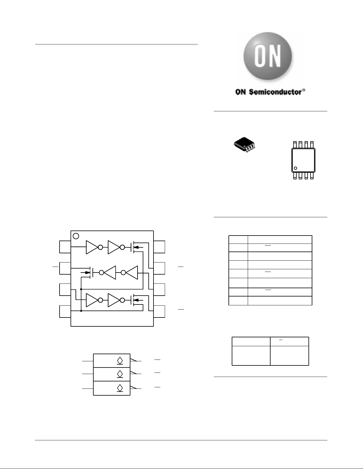
NL37WZ06
Triple Inverter with Open
Drain Outputs
The NL37WZ06 is a high performance triple inverter with open
drain outputs operating from a 1.65 to 5.5 V supply.
The internal circuit is composed of multiple stages, including an
open drain output which provides the capability to set output
switching level. This allows the NL37WZ06 to be used to interface 5
V circuits to circuits of any voltage between V
external resistor and power supply .
• Extremely High Speed: t
• Designed for 1.65 V to 5.5 V V
2.5 ns (typical) at VCC = 5 V
PD
Operation
CC
• Over Voltage Tolerant Inputs
• LVTTL Compatible − Interface Capability with 5 V TTL Logic with
VCC = 3 V
• LVCMOS Compatible
• 24 mA Output Sink Capability @ 3.0 V
• Near Zero Static Supply Current Substantially Reduces System
Power Requirements
• Chip Complexity: FET = 72
and 7 V using an
CC
http://onsemi.com
8
1
US8
US SUFFIX
CASE 493
LF = Device Code
D = Date Code
MARKING
DIAGRAM
8
D
LF
1
IN A1
OUT Y3
IN A2
GND
PIN ASSIGNMENT
1
1
2
3
45
8
7
6
V
CC
OUT Y1
IN A3
OUT Y2
2
3IN A2
4
5
6
7
8
FUNCTION TABLE
Figure 1. Pinout (Top View)
IN A1
IN A2
IN A3
1
1
1
Figure 2. Logic Symbol
OUT Y1
OUT Y2
OUT Y3
See detailed ordering and shipping information in the package
dimensions section on page 4 of this data sheet.
A Input Y Output
ORDERING INFORMATION
IN A1
OUT Y3
GND
OUT Y2
IN A3
OUT Y1
V
L
H
CC
Z
L
Semiconductor Components Industries, LLC, 2003
August, 2003 − Rev. 2
1 Publication Order Number:
NL37WZ06/D
NL37WZ06
MAXIMUM RATINGS
Symbol Parameter Value Unit
V
CC
V
I
V
O
I
IK
I
OK
I
O
I
CC
I
GND
T
STG
T
L
T
J
JA
P
D
MSL Moisture Sensitivity Level 1
F
R
V
ESD
Maximum Ratings are those values beyond which damage to the device may occur. Exposure to these conditions or conditions beyond those
indicated may adversely affect device reliability. Functional operation under absolute maximum−rated conditions is not implied. Functional
operation should be restricted to the Recommended Operating Conditions.
1. Measured with minimum pad spacing on an FR4 board, using 10 mm−by−1 inch, 2−ounce copper trace with no air flow.
2. Tested to EIA/JESD22−A114−A.
3. Tested to EIA/JESD22−A115−A.
4. Tested to JESD22−C101−A.
DC Supply Voltage −0.5 to +7.0 V
DC Input Voltage −0.5 to 7.0 V
DC Output Voltage −0.5 to 7.0 V
DC Input Diode Current VI < GND −50 mA
DC Output Diode Current VO < GND −50 mA
DC Output Sink Current 50 mA
DC Supply Current per Supply Pin 100 mA
DC Ground Current per Ground Pin 100 mA
Storage Temperature Range −65 to +150 °C
Lead Temperature, 1 mm from Case for 10 Seconds 260 °C
Junction Temperature under Bias +150 °C
Thermal Resistance (Note 1) 250 °C/W
Power Dissipation in Still Air at 85°C 250 mW
Flammability Rating Oxygen Index: 28 to 34 UL 94 V−0 @ 0.125 in
ESD Withstand Voltage Human Body Model (Note 2)
Machine Model (Note 3)
Charged Device Model (Note 4)
> 2000
> 200
N/A
V
RECOMMENDED OPERATING CONDITIONS
Symbol Parameter Min Max Unit
V
CC
V
I
V
O
T
A
t/V Input Transition Rise or Fall Rate VCC = 2.5 V 0.2 V
5. Unused inputs may not be left open. All inputs must be tied to a high− or low−logic input voltage level.
Supply Voltage Operating
Data Retention Only
1.65
1.5
5.5
5.5
Input Voltage (Note 5) 0 5.5 V
Output Voltage (HIGH or LOW State) 0 V
CC
Operating Free−Air Temperature −40 85 °C
VCC = 3.0 V 0.3 V
V
= 5.0 V 0.5 V
CC
0
0
0
20
10
5
V
V
ns/V
http://onsemi.com
2
DC ELECTRICAL CHARACTERISTICS
V
CC
V
IN
V
IH
V
IL
Î
Î
Î
Î
Î
Î
Î
Î
Î
Î
Î
Î
Î
Î
Î
Î
Î
Î
Î
Î
Î
Î
Î
Î
Î
Î
Î
Î
Î
Î
Î
Î
Î
Î
Î
Î
Î
Î
Î
Î
Î
Î
Î
Î
Î
Î
Î
Î
Î
Î
Î
Î
Î
Î
Î
Î
Î
Î
Symbol Parameter Condition
V
V
I
V
I
I
I
IH
IL
LKG
OL
IN
OFF
CC
High−Level Input Voltage 1.65
Low−Level Input Voltage 1.65
Z−State Output
Leakage Current
Low−Level Output Voltage
= VIH or V
V
or
IN
IL
VIN = V
V
= VCC or GND
OUT
IOL = 100 A 1.65 to 5.5 0.1 0.1
IOL = 4 mA 1.65 0.45 0.45
IOL = 8 mA 2.3 0.22 0.3 0.3
IOL = 12 mA 2.7 0.22 0.4 0.4
IOL = 16 mA 3.0 0.28 0.4 0.4
IOL = 24 mA 3.0 0.38 0.55 0.55
IOL = 32 mA 4.5 0.42 0.55 0.55
Input Leakage Current VIN or V
Power Off−Output
Leakage Current
Quiescent Supply Cur-
VIN = VCC or GND 5.5 1.0 10 A
= VCC or
OUT
GND
V
= 5.5 V 0 1.0 10 A
OUT
rent
NL37WZ06
V
(V)
0.75 V
2.3 to 5.5
0.7 V
2.3 to 5.5
IL
1.65 to 5.5 ±5.0 ±10.0 A
0 to 5.5 ±0.1 ±1.0 A
TA = 25°C −40°C ≤ TA ≤ 85°C
Min Typ Max Min Max
CC
CC
0.75 V
0.7 V
CC
CC
0.25 V
0.3 V
CC
CC
0.25 V
0.3 V
CC
CC
Unit
V
V
V
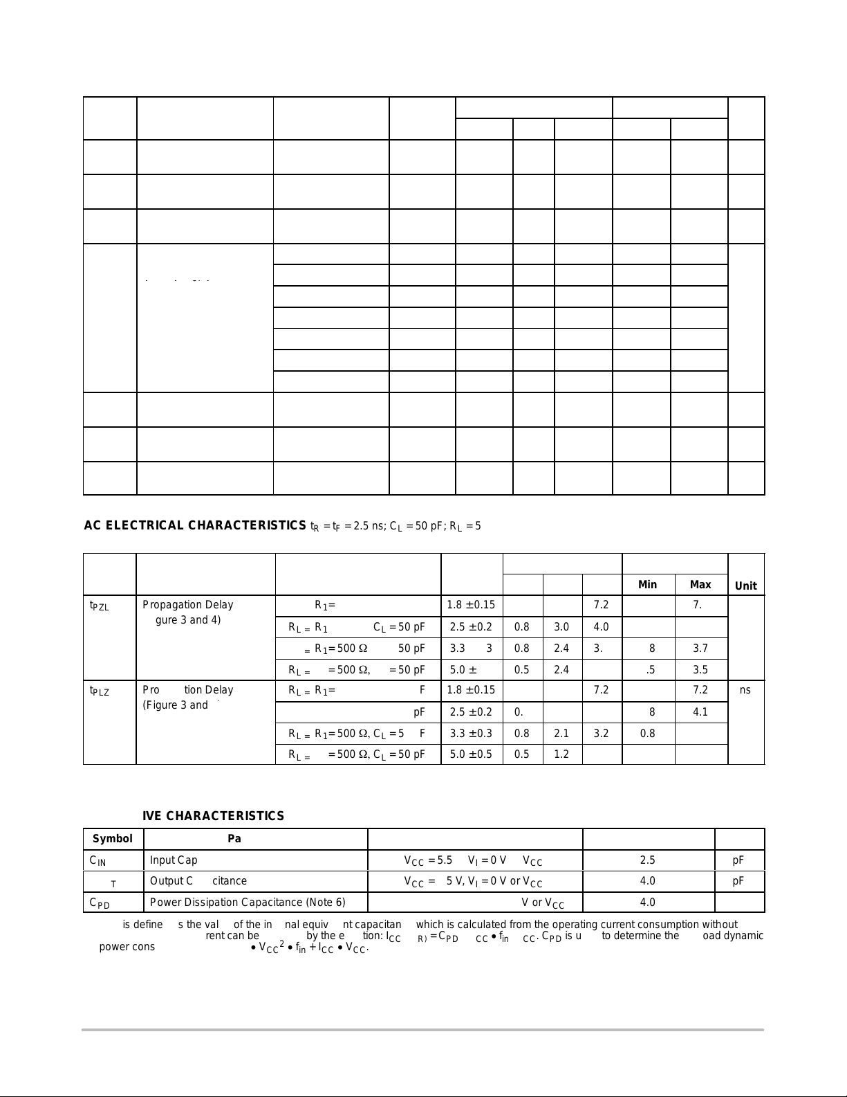
AC ELECTRICAL CHARACTERISTICS t
Symbol
ÎÎ
t
PZL
ÎÎ
ÎÎÎООООО
ÎÎÎОООООÎООООООО
ÎÎÎОООООÎООООООО
t
PLZ
ÎÎ
ÎÎÎООООО
ÎÎÎОООООÎООООООО
Parameter
ООООО
Propagation Delay
ООООО
(Figure 3 and 4)
Propagation Delay
ООООО
(Figure 3 and 4)
ООООООО
ООООООО
ООООООО
ООООООО
ООООООО
= tF = 2.5 ns; CL = 50 pF; RL = 500
R
Condition
R
R1= 500 C
L =
R
R1= 500 C
L =
R
R1= 500 C
L =
R
R1= 500 C
L =
R
R1= 500 C
L =
R
R1= 500 C
L =
R
R1= 500 C
L =
R
R1= 500 C
L =
= 50 pF
L
= 50 pF
L
= 50 pF
L
= 50 pF
L
= 50 pF
L
= 50 pF
L
= 50 pF
L
= 50 pF
L
VCC (V)
ÎÎ
1.8 ± 0.15
ÎÎ
2.5 ± 0.2
ÎÎ
3.3 ± 0.3
ÎÎ
5.0 ± 0.5
ÎÎ
1.8 ± 0.15
ÎÎ
2.5 ± 0.2
ÎÎ
3.3 ± 0.3
ÎÎ
5.0 ± 0.5
TA = 25°C
Min
Typ
Î
ÎÎÎÎÎ
0.8
Î
0.8
Î
0.5
Î
ÎÎÎÎÎ
0.8
Î
0.8
Î
0.5
Î
3.0
Î
2.4
Î
2.4
Î
2.5
Î
2.1
Î
1.2
Max
Î
7.2
4.0
Î
3.2
Î
3.0
Î
7.2
4.0
Î
3.2
Î
3.0
−40°C ≤ TA ≤ 85°C
Min
Î
ÎÎÎÎ
0.8
Î
0.8
Î
0.5
Î
ÎÎÎÎ
0.8
Î
0.8
Î
0.5
Max
ÎÎ
7.2
4.1
ÎÎ
3.7
ÎÎ
3.5
ÎÎ
7.2
4.1
ÎÎ
3.7
ÎÎ
3.5
Unit
ns
ns
CAPACITIVE CHARACTERISTICS
Symbol Parameter Condition Typical Unit
C
IN
C
OUT
C
PD
6. CPD is defined as the value of the internal equivalent capacitance which is calculated from the operating current consumption without load.
Average operating current can be obtained by the equation: I
power consumption; P
Input Capacitance VCC = 5.5 V, VI = 0 V or V
Output Capacitance VCC = 5.5 V, VI = 0 V or V
CC
CC
Power Dissipation Capacitance (Note 6) 10 MHz, VCC = 5.5 V, VI = 0 V or V
= CPD VCC fin + ICC. CPD is used to determine the no−load dynamic
)
= CPD V
D
2
fin + ICC VCC.
CC
CC(OPR
CC
2.5 pF
4.0 pF
4.0 pF
http://onsemi.com
3

PULSE
GENERATOR
NL37WZ06
A
Y
50%
t
PZLtPLZ
50% V
CC
Figure 3. Switching Waveforms
V
CC
DUT
R
T
V
+0.3 V
OL
V
CC
GND
HIGH
IMPEDANCE
R
C
R
L
L
1
VCC x 2
RT = Z
of pulse generator (typically 50 )
OUT
Figure 4. Test Circuit
DEVICE ORDERING INFORMATION
Device Nomenclature
Logic
Device
Order Number
Circuit
Indicator
NL37WZ06US NL 3 7 WZ 06 US US8
No. of
Gates
per
Package
Temp
Range
Identifier
Technology
Device
Function
Package
Suffix
Package Type
Tape and
Reel Size
178 mm (7″)
3000 Unit
http://onsemi.com
4

NL37WZ06
CAVITY
TAPE
TOP TAPE
TAPE DIMENSIONS mm
8.00
+ 0.30
− 0.10
TAPE TRAILER
(Connected to Reel Hub)
NO COMPONENTS
160 mm MIN
Figure 5. Tape Ends for Finished Goods
4.00
2.00
4.00
COMPONENTS
DIRECTION OF FEED
TAPE LEADER
NO COMPONENTS
400 mm MIN
1.50 TYP
1.75
3.50 0.25
1
1.00 ± 0.25 TYP
DIRECTION OF FEED
Figure 6. US8 Reel Configuration/Orientation
http://onsemi.com
5

NL37WZ06
1.5 mm MIN
(0.06 in)
(0.512 in 0.008 in)
t MAX
13.0 mm 0.2 mm
20.2 mm MIN
A
(0.795 in)
REEL DIMENSIONS
Tape Size
8 mm
T and R Suffix
FULL RADIUS
Figure 7. Reel Dimensions
A Max
US
178 mm
(7 in)
DIRECTION OF FEED
G
8.4 mm, + 1.5 mm, −0.0
(0.33 in + 0.059 in, −0.00)
50 mm MIN
(1.969 in)
G
t Max
14.4 mm
(0.56 in)
BARCODE LABEL
Figure 8. Reel Winding Direction
http://onsemi.com
6
HOLEPOCKET

−T−
SEATING
PLANE
A
58
P
D
G
K
0.10 (0.004) XY
M
41
−X−
LB
T
−Y−
C
NL37WZ06
PACKAGE DIMENSIONS
US8
US SUFFIX
CASE 493−02
ISSUE A
J
DETAIL E
R
S
U
T0.10 (0.004)
V
DETAIL E
H
N
F
NOTES:
R 0.10 TYP
M
1. DIMENSIONING AND TOLERANCING PER
ANSI Y14.5M, 1982.
2. CONTROLLING DIMENSION: MILLIMETERS.
3. DIMENSION “A” DOES NOT INCLUDE MOLD
FLASH, PROTRUSION OR GATE BURR.
MOLD FLASH. PROTRUSION AND GATE
BURR SHALL NOT EXCEED 0.140 MM
(0.0055”) PER SIDE.
4. DIMENSION “B” DOES NOT INCLUDE
INTER−LEAD FLASH OR PROTRUSION.
INTER−LEAD FLASH AND PROTRUSION
SHALL NOT E3XCEED 0.140 (0.0055”) PER
SIDE.
5. LEAD FINISH IS SOLDER PLATING WITH
THICKNESS OF 0.0076−0.0203 MM.
(300−800 “).
6. ALL TOLERANCE UNLESS OTHERWISE
SPECIFIED ±0.0508 (0.0002 “).
MILLIMETERS
DIMAMIN MAX MIN MAX
1.90 2.10 0.075 0.083
B 2.20 2.40 0.087 0.094
C 0.60 0.90 0.024 0.035
D 0.17 0.25 0.007 0.010
F 0.20 0.35 0.008 0.014
G 0.50 BSC 0.020 BSC
H 0.40 REF 0.016 REF
J 0.10 0.18 0.004 0.007
K 0.00 0.10 0.000 0.004
L 3.00 3.20 0.118 0.126
M 0 6 0 6
N 5 10 5 10
P 0.23 0.34 0.010 0.013
R 0.23 0.33 0.009 0.013
S 0.37 0.47 0.015 0.019
U 0.60 0.80 0.024 0.031
V 0.12 BSC
INCHES
0.005 BSC
0.5 TYP
3.8
1.8 TYP
1.0
0.3 TYP
(mm)
http://onsemi.com
7

NL37WZ06
ON Semiconductor and are registered trademarks of Semiconductor Components Industries, LLC (SCILLC). SCILLC reserves the right to make
changes without further notice to any products herein. SCILLC makes no warranty, representation or guarantee regarding the suitability of its products for any
particular purpose, nor does SCILLC assume any liability arising out of the application or use of any product or circuit, and specifically disclaims any and all
liability, including without limitation special, consequential or incidental damages. “Typical” parameters which may be provided in SCILLC data sheets and/or
specifications can and do vary in different applications and actual performance may vary over time. All operating parameters, including “Typicals” must be
validated for each customer application by customer’s technical experts. SCILLC does not convey any license under its patent rights nor the rights of others.
SCILLC products are not designed, intended, or authorized for use as components in systems intended for surgical implant into the body, or other applications
intended to support or sustain life, or for any other application in which the failure of the SCILLC product could create a situation where personal injury or death
may occur. Should Buyer purchase or use SCILLC products for any such unintended or unauthorized application, Buyer shall indemnify and hold SCILLC
and its officers, employees, subsidiaries, affiliates, and distributors harmless against all claims, costs, damages, and expenses, and reasonable attorney fees
arising out of, directly or indirectly, any claim of personal injury or death associated with such unintended or unauthorized use, even if such claim alleges that
SCILLC was negligent regarding the design or manufacture of the part. SCILLC is an Equal Opportunity/Affirmative Action Employer.
PUBLICATION ORDERING INFORMATION
Literature Fulfillment:
Literature Distribution Center for ON Semiconductor
P.O. Box 5163, Denver, Colorado 80217 USA
Phone: 303−675−2175 or 800−344−3860 Toll Free USA/Canada
Fax: 303−675−2176 or 800−344−3867 Toll Free USA/Canada
Email: orderlit@onsemi.com
N. American Technical Support: 800−282−9855 Toll Free USA/Canada
http://onsemi.com
JAPAN: ON Semiconductor, Japan Customer Focus Center
2−9−1 Kamimeguro, Meguro−ku, Tokyo, Japan 153−0051
Phone: 81−3−5773−3850
ON Semiconductor Website: http://onsemi.com
For additional information, please contact your local
Sales Representative.
NL37WZ06/D
8
 Loading...