

Page 1
3-19
3
GENERAL PURPOSE
AMPLIFIERS (LNAs,
HPAs, LINEAR AMPS)
Optimum Technology Matching® Applied
GaAs HBT
InGaP HBT
GaAs MESFET
SiGe BiCMOS
Si BiCMOS
SiGe HBT
GaAs pHEMT
Si CMOS
Si BJT
GaN HEMT
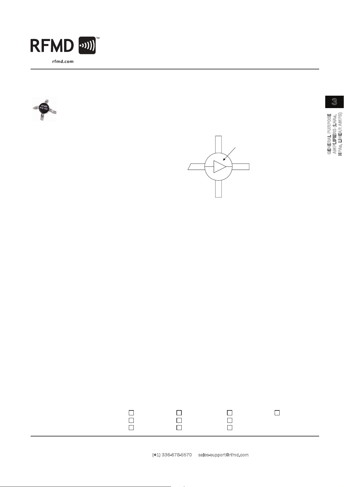
Functional Block Diagram
RF MICRO DEVICES®, RFMD®, Optimum Technology Matching®, Enabling Wireless Connectivity™, PowerStar®, POLA RIS™ TOTAL RADIO™ and UltimateBlue™ are trademarks of RFMD, LLC. BLUETOOTH is a trade-
mark owned by Bluetooth SIG, Inc., U.S.A. and licensed for use by RFMD. All other trade names, trademarks and registered trademarks are the property of their respective own ers. ©2006, RF Micro Devices, Inc.
Product Description
7628 Thorndike Road, Greensboro, NC 27409-9421 · For sales or technical
support, contact RFMD at (
+1) 336-678-5570 or [email protected].
Ordering Information
1 3
2
4
RF OUTRF OUTRF IN
GND
GND
MARKING - N3
NLB-300
CASCADABLE BROADBAND
GaAs MMIC AMPLIFIER DC TO 10GHz
The NLB-300 cascadable broadband InGaP/GaAs MMIC amplifier is a lowcost, high-performance solution for general purpose RF and microwave
amplification needs. This 50! gain block is based on a reliable HBT proprietary MMIC design, providing unsurpassed performance for small-signal applications. Designed with an external bias resistor, the NLB-300
provides flexibility and stability. The NLB-300 is packaged in a low-cost,
surface-mount plastic package, providing ease of assembly for high-volume tape-and-reel requirements.
Features
! Reliable, Low-Cost HBT
Design
! 13.0 dB Gain, +11.1dBm
P1dB@2GHz
!
High P1dB of
[email protected] and
[email protected]
! Single Power Supply Opera-
tion
! 50 ! I/O Matched for High
Freq. Use
Applications
! Narrow and Broadband Com-
mercial and Military Radio
Designs
! Linear and Saturated Amplifi-
ers
! Gain Stage or Driver Amplifi-
ers for MWRadio/Optical
Designs (PTP/PMP/
LMDS/UNII/VSAT/WLAN/Cellular/DWDM)
NLB-300Cascadable Broadband GaAs MMIC Amplifier DC to 10GHz
NLB-300 Cascadable Broadband GaAs MMIC Amplifier DC to 10GHz
NLB-300-T1 Tape & Reel, 1000 Pieces
NLB-300-E Fully Assembled Evaluation Board
NBB-X-K1 Extended Frequency InGaP Amp Designer’s Tool Kit
Rev A10 DS070123
"
NLB-300Cascadable
Broadband
GaAs MMIC
Amplifier DC to
10GHz
RoHS Compliant & Pb-Free Product
Package Style: Micro-X, 4-Pin, Plastic
Page 2
NLB-300
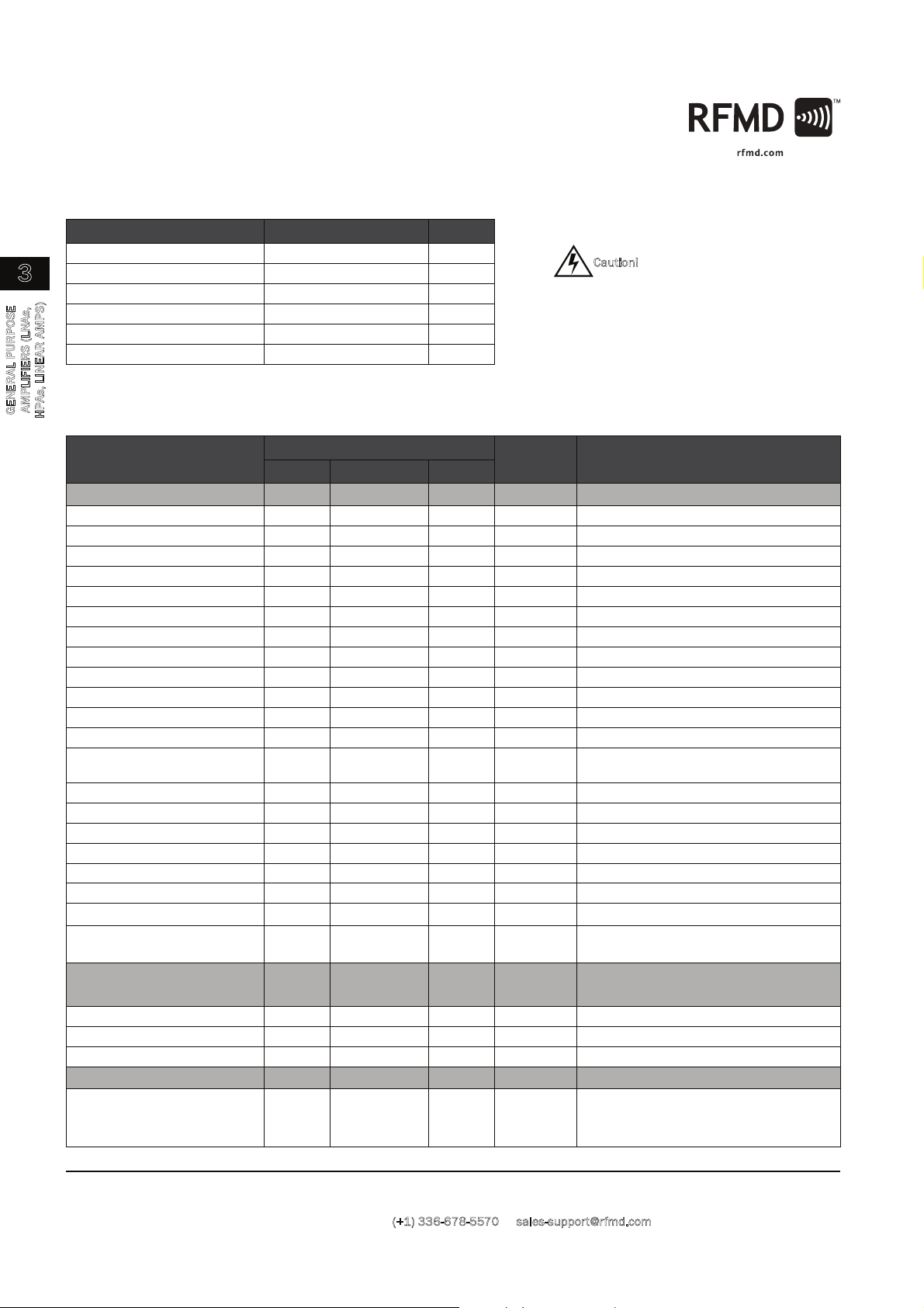
Absolute Maximum Ratings
Parameter Rating Unit
RF Input Power +20 dBm
3
GENERAL PURPOSE
Power Dissipation 300 mW
Device Current 70 mA
Channel Temperature 200 °C
Operating Temperature -45 to +85 °C
Storage Temperature -65 to +150 °C
Exceeding any one or a combination of these limits may cause permanent
damage.
MPLIFIERS (LNAs,
A
HPAs, LINEAR AMPS)
The information in this publication is believed to be accurate and reliable. However, no responsibility is assumed by RF Micro Devices, Inc. ("RFMD") for its use,
nor for any infringement of patents, or other rights of third parties, resulting
from its use. No license is granted by implication or otherwise under any patent
or patent rights of RFMD. RFMD reserves the right to change component circuitry, recommended application circuitry and specifications at any time without
prior notice.
RoHS status based on EUDirective 2002/95/EC (at time of this document revision).
Caution! ESD sensitive device.
Parameter
Min. Typ. Max.
Overall
Small Signal Power Gain, S21 12.0 13.0 dB f=0.1GHz to 1.0 GHz
Gain Flatness, GF ±0.1 dB f= 5.0GHz to 10.0GHz
Input VSWR 2.2:1 f=0.1GHz to 4.0 GHz
Output VSWR 2.2:1 f=0.1GHz to 4.0 GHz
Output Power @
-1dB Compression, P1dB 11.1 dBm f=2.0GHz
Noise Figure, NF 4.9 dB f=3.0GHz
Third Order Intercept, IP3 +28.6 dBm f= 2.0GHz
Reverse Isolation, S12 -16 dB f= 0.1GHz to 20.0 GHz
Device Voltage, V
Gain Temperature Coefficient,
"GT/"T
3.6 3.8 4.2 V
D
Specification
10.7 dB f= 1.0GHz to 4.0GHz
8.9 dB f=4.0GHz to 6.0GHz
8.5 8.9 dB f=6.0GHz to 10.0GHz
8.5 dB f=10.0GHz to 12.0 GHz
2.8:1 f=4.0GHz to 7.0GHz
2.0:1 f=7.0GHz to 12.0GHz
2.9:1 f=4.0GHz to 7.0GHz
2.4:1 f=7.0GHz to 12.0GHz
14.1 dBm f=6.0GHz
12.7 dBm f= 10.0GHz
+27.0 f= 6.0GHz
-0.0015 dB/°C
Unit Condition
VD=+3.8V, ICC=50mA, Z0=50!, TA=+25°C
MTTF versus Temperature
@ ICC=50mA
Case Temperature 85 °C
Junction Temperature 113 °C
MTTF >1,000,000 hours
Thermal Resistance
#JC 147 °C/W
JTT
–
CAS E
---------------------------
VDICC$
#JC%C Wat t&' (=
3-20
7628 Thorndike Road, Greensboro, NC 27409-9421 · For sales or technical
support, contact RFMD at (+1) 336-678-5570 or [email protected].
Rev A10 DS070123
Page 3
NLB-300
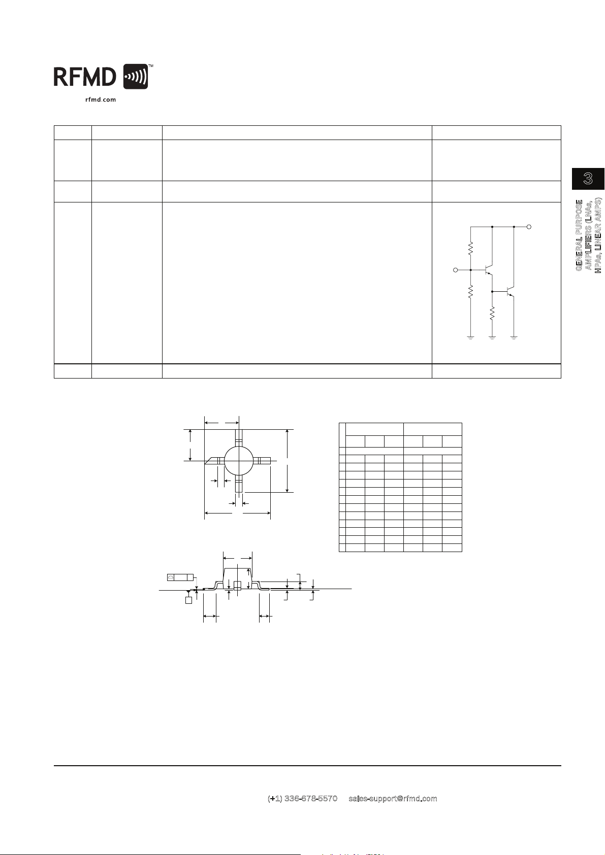
Package Drawing
Pin Function Description Interface Schematic
1 RF IN
RF input pin. This pin is NOT internally DC-blocked. A DC-blocking capacitor,
suitable for the frequency of operation, should be used in most applications. DC coupling of the input is not allowed, because this will override the
internal feedback loop and cause temperature instability.
2 GND
Ground connection. For best performance, keep traces physically short
and connect immediately to ground plane.
3 RF OUT
RF output and bias pin. Biasing is accomplished with an external series
resistor and choke inductor to VCC. The resistor is selected to set the DC
current into this pin to a desired level. The resistor value is determined by
the following equation:
Care should also be taken in the resistor selection to ensure that the current into the part never exceeds maximum datasheet operating current
over the planned operating temperature. This means that a resistor
between the supply and this pin is always required, even if a supply near
5.0V is available, to provide DC feedback to prevent thermal runaway.
Because DC is present on this pin, a DC-blocking capacitor, suitable for the
frequency of operation, should be used in most applications. The supply
side of the bias network should also be well bypassed.
4 GND
Same as pin 2.
R
V
CCVDEVIC E
–' (
I
CC
-------------------------------------------
=
RF OUT
RF IN
B
N 5
C
A
D
4 M
S
Seating Plane
0.08 S
6
F
E
1 J
2
Kx 3L 3
H
0.1G
Gauge Plane
Symbol
A
B
C
D
E
F
G
H
J
1
K
2
L
3
M
4
N
5
0.535 REF.
MILLIMETERS INCHES
Min. Nom. Max. Min. Nom. Max.
0.021 REF.
2.39 2.54 2.69 0.094 0.100 0.106
0.436 0.510 0.586 0.017 0.020 0.023
2.19 2.34 2.49 0.086 0.092 0.098
1.91 2.16 2.41 0.075 0.085 0.095
1.32 1.52 1.72 0.052 0.060 0.068
0.10 0.15 0.20 0.004 0.006 0.008
0.535 0.660 0.785 0.021 0.026 0.031
0.05 0.10 0.15 0.002 0.004 0.006
0.65 0.75 0.85 0.025 0.029 0.033
0.85 0.95 1.05 0.033 0.037 0.041
4.53 4.68 4.83 0.178 0.184 0.190
4.73 4.88 5.03 0.186 0.192 0.198
NOTE: All dimensions are in millimeters, and
the dimensions in inches are for reference only.
3
AMPLIFIERS (LNAs,
GENERAL PURPOSE
HPAs, LINEAR AMPS)
Rev A10 DS070123
7628 Thorndike Road, Greensboro, NC 27409-9421 · For sales or technical
support, contact RFMD at (
+1) 336-678-5570 or [email protected].
3-21
Page 4
3
NLB-300
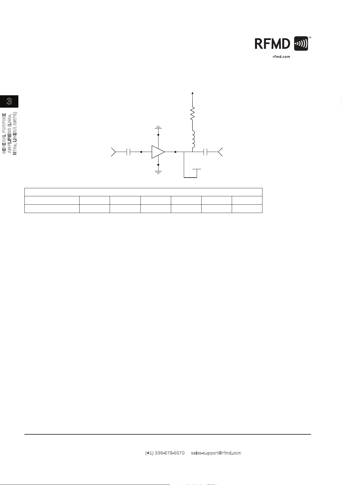
Typical Bias Configuration
Application notes related to biasing circuit, device footprint, and thermal considerations are available on request.
V
CC
R
CC
4
MPLIFIERS (LNAs,
A
GENERAL PURPOSE
HPAs, LINEAR AMPS)
In Out
1 3
C block
2
Recommended Bias Resistor Values
Supply Voltage, VCC (V) 5 8 10 12 15 20
Bias Resistor, RCC (!) 22 82 122 162 222 322
V
DEVICE
L choke
(optional)
C block
3-22
7628 Thorndike Road, Greensboro, NC 27409-9421 · For sales or technical
support, contact RFMD at (+1) 336-678-5570 or [email protected].
Rev A10 DS070123
Page 5
NLB-300
Extended Frequency InGaP Amplifier Designer’s Tool Kit
NBB-X-K1
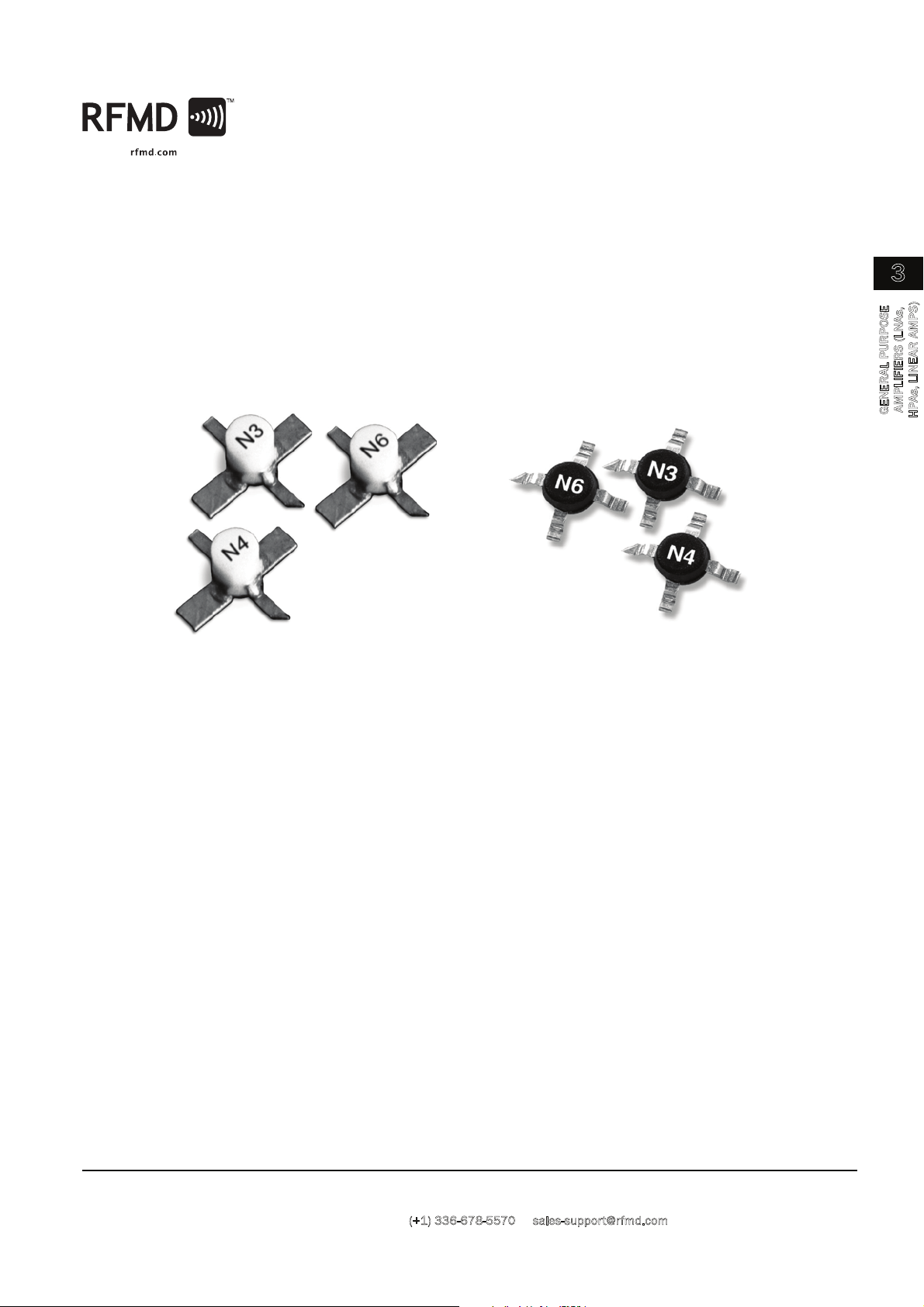
This tool kit was created to assist in the design-in of the RFMD NBB- and NLB-series InGap HBT gain block amplifiers. Each tool
kit contains the following.
• 5 each NBB-300, NBB-310 and NBB-400 Ceramic Micro-X Amplifiers
• 5 each NLB-300, NLB-310 and NLB-400 Plastic Micro-X Amplifiers
• 2 Broadband Evaluation Boards and High Frequency SMA Connectors
• Broadband Bias Instructions and Specification Summary Index for ease of operation
3
AMPLIFIERS (LNAs,
GENERAL PURPOSE
HPAs, LINEAR AMPS)
Rev A10 DS070123
7628 Thorndike Road, Greensboro, NC 27409-9421 · For sales or technical
support, contact RFMD at (
+1) 336-678-5570 or [email protected].
3-23
Page 6
3
GENERAL PURPOSE
A
MPLIFIERS (LNAs,
HPAs, LINEAR AMPS)
3-24
NLB-300
Rev A10 DS070123
7628 Thorndike Road, Greensboro, NC 27409-9421 · For sales or technical
support, contact RFMD at (+1) 336-678-5570 or [email protected].
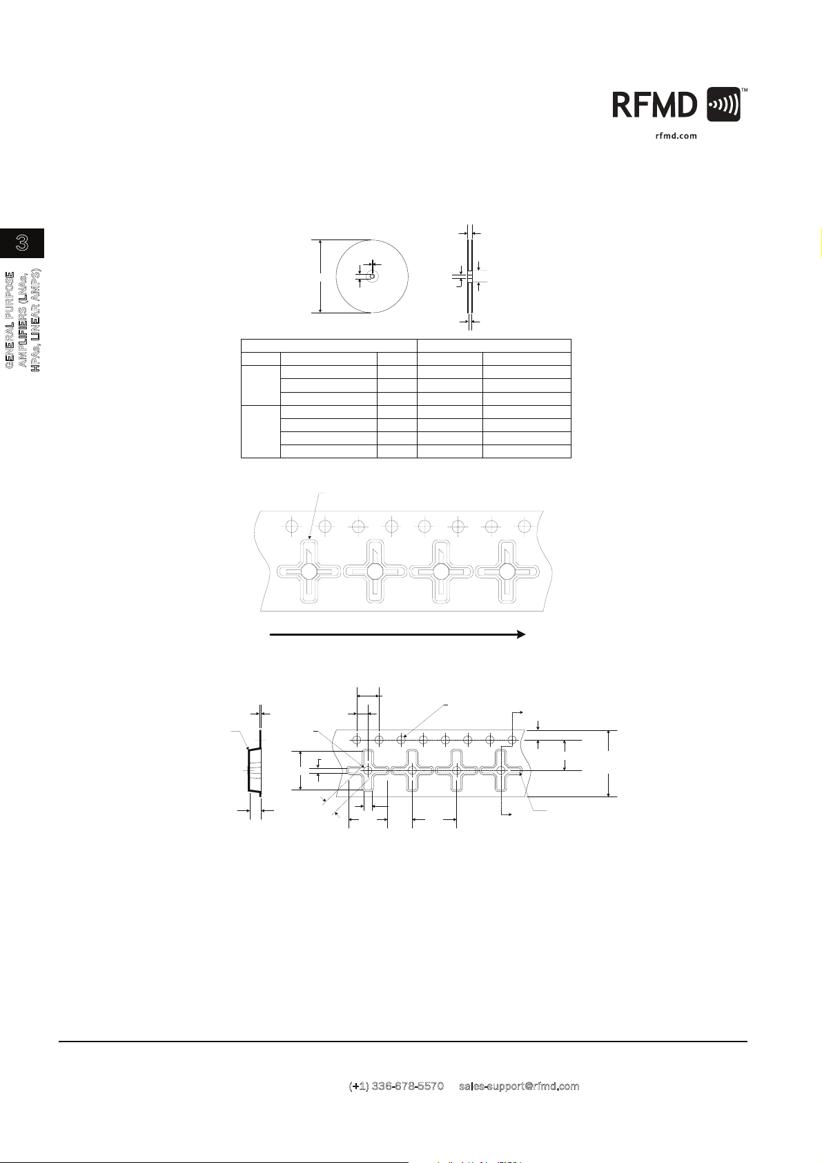
Tape and Reel Dimensions
All Dimensions in Millimeters
Ao = 7.0 MM
A1 = 1.8 MM
Bo = 7.0 MM
B1 = 1.3 MM
Ko = 2.1 MM
NOTES:
1. 10 sprocket hole pitch cumulative tolerance ±0.2.
2. Camber not to exceed 1 mm in 100 mm.
3. Material: PS+C.
4. Ao and Bo measured on a plane 0.3 mm above the bottom of the pocket.
5. Ko measured from a plane on the inside bottom of the pocket to the surface of the carrier.
6. Pocket position relative to sprocket hole measured as true position of pocket, not pocket hole.
A
A
SECTION A-A
8.0
Ao
A1
3.0
B1
Bo
5.0 MIN.
2.00 ± 0.05
SEE NOTE 6
4.0
SEE NOTE 1
R0.3 MAX.
0.30
± 0.05
All dimensions in mm
12.0
± 0.3
5.50 ± 0.05
SEE NOTE 6
1.75
R0.3 TYP.Ko
5.0
+0.1
-0.0
User Direction of Feed
LEAD 1
N3
N3
N3
N3
O
S
F
T
B
A
D
7.0 +0.079/-0.158
0.724 MAX
0.50 +0.08
3.0 REF
0.540 +0.020/-0.008
0.059 MIN
0.795 MIN
Plastic, Micro-X
SIZE (inches)
178 +0.25/-4.0
18.4 MAX
12.8 +2.0
76.2 REF
13.716 +0.5/-0.2
1.5 MIN
20.2 MIN
SIZE (mm)
FLANGE
B
T
F
Diameter
Thickness
Space Between Flange
HUB
O
S
A
Outer Diameter
Spindle Hole Diameter
Key Slit Width
DKey Slit Diameter
14.732 mm (7") REEL
SYMBOLITEMS
Page 7
NLB-300
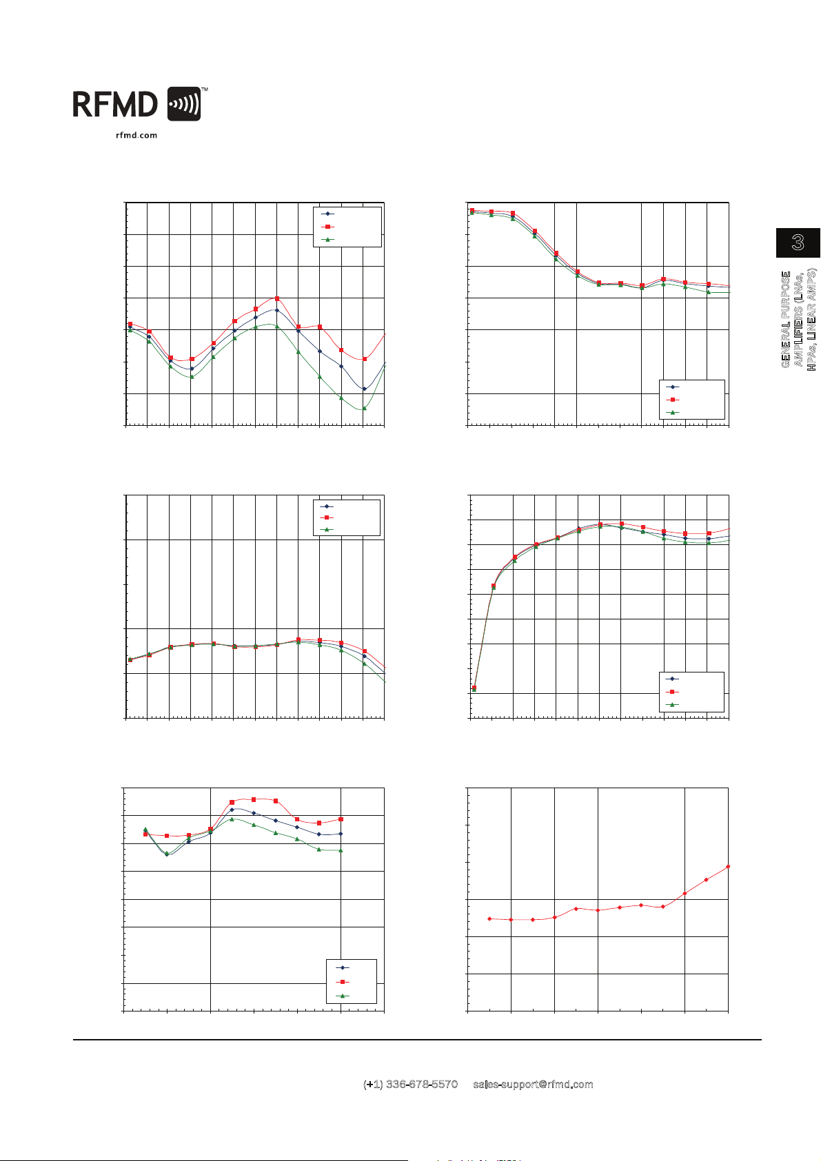
Output P1dB versus Frequency Across Temperature
0.0
2.0
4.0
6.0
8.0
10.0
12.0
14.0
16.0
0.0 2.0 4.0 6.0 8.0 10.0 12.0
Frequency (GHz)
Output P1dB (dBm)
25°C
40°C
85°C
Noise Frequency versus Frequency at +25°C
0.0
2.0
4.0
6.0
8.0
10.0
12.0
0.0 2.0 4.0 6.0 8.0 10.0 12.0
Frequency (GHz)
Noise Figure (dB)
S11 versus Frequency, Over Temperature
-14.0
-12.0
-10.0
-8.0
-6.0
-4.0
-2.0
0.0
0.0 1.0 2.0 3.0 4.0 5.0 6.0 7.0 8.0 9.0 10.0 11.0 12.0
Frequency (GHz)
S21 (dB)
S11, +25°C
S11, -40°C
S11, +85°C
S21 versus Frequency, Over Temperature
0.0
2.0
4.0
6.0
8.0
10.0
12.0
14.0
0.0 1.0 2.0 3.0 4.0 5.0 6.0 7.0 8.0 9.0 10.0 11.0 12.0
Frequency (GHz)
S21 (dB)
S21, +25°C
S21, -40°C
S21, +85°C
S12 versus Frequency, Over Temperature
-25.0
-20.0
-15.0
-10.0
-5.0
0.0
0.0 1.0 2.0 3.0 4.0 5.0 6.0 7.0 8.0 9.0 10.0 11.0 12.0
Frequency (GHz)
S21 (dB)
S12, +25°C
S12, -40°C
S12, +85°C
S22 versus Frequency, Over Temperature
-45.0
-40.0
-35.0
-30.0
-25.0
-20.0
-15.0
-10.0
-5.0
0.0
0.0 1.0 2.0 3.0 4.0 5.0 6.0 7.0 8.0 9.0 10.0 1 1.0 12.0
Frequency (GHz)
S22 (dB)
S11, +25°C
S11, -40°C
S11, +85°C
3
AMPLIFIERS (LNAs,
GENERAL PURPOSE
HPAs, LINEAR AMPS)
Rev A10 DS070123
7628 Thorndike Road, Greensboro, NC 27409-9421 · For sales or technical
support, contact RFMD at (
+1) 336-678-5570 or [email protected].
3-25
Page 8
3
NLB-300
Note: The s-parameter gain results shown include device performance as well as evaluation board and connector loss variations. The insertion losses of the evaluation board and connectors are as follows:
1GHz to 4GHz=-0.06 dB
5GHz to 9GHz=-0.22 dB
10GHz to 14GHz= -0.50dB
15GHz to 20GHz= -1.08dB
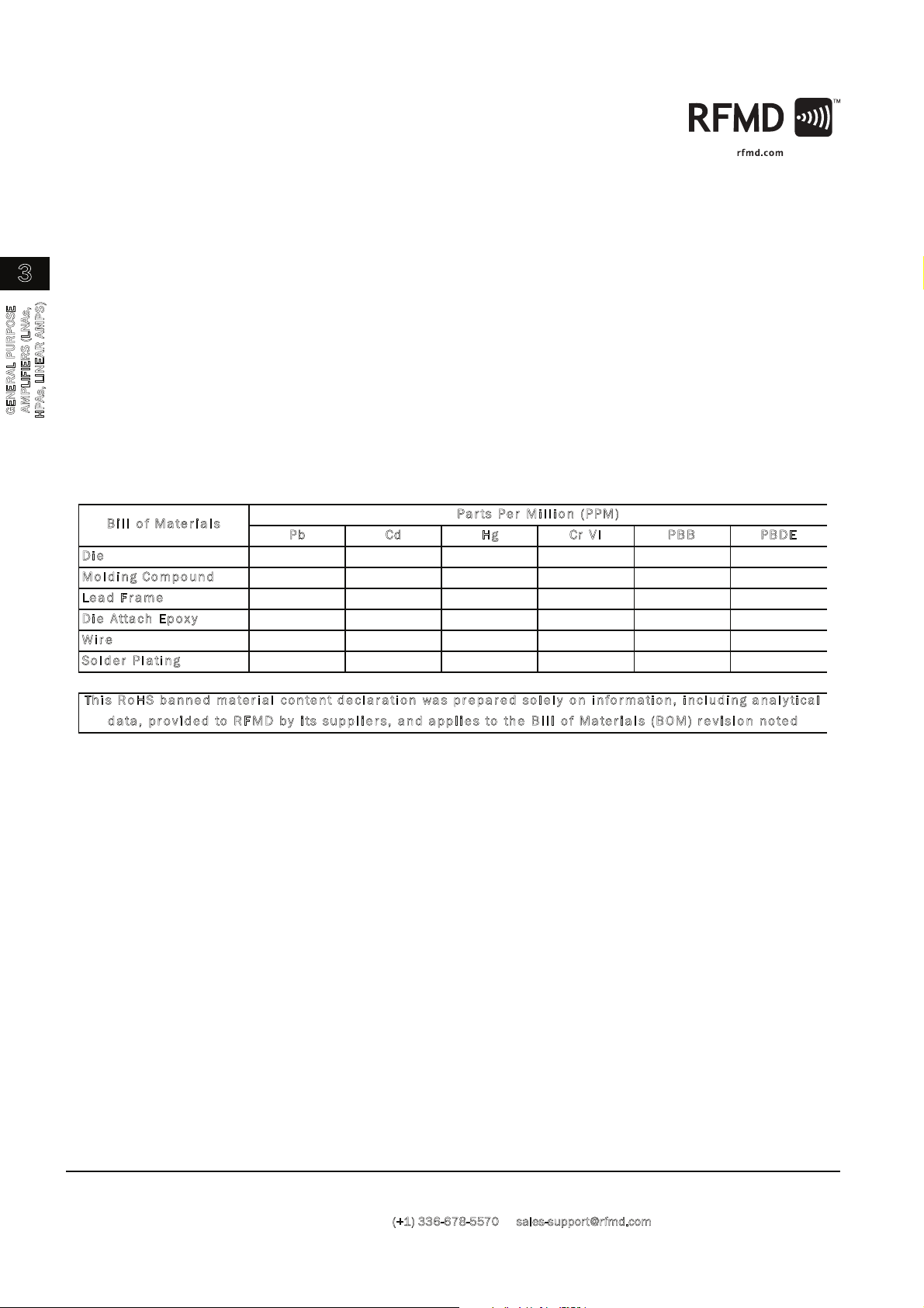
RoHS* Banned Material Content
MPLIFIERS (LNAs,
A
GENERAL PURPOSE
RoHS Compliant: Yes
Package total weight in grams (g): 0.024
HPAs, LINEAR AMPS)
Compliance Date Code: 0601
Bill of Materials Revision: -
Pb Free Category: e3
B ill o f Ma ter ia l s
Die 0 0 0 0 0 0
Mol di ng Comp o un d 0 0 0 0 0 0
Le a d F ra me 0 0 0 0 0 0
D
i e Attach Ep o xy 0 0 0 0 0 0
i r e 0 0 0 0 0 0
W
S
olde r Plating 0 0 0 0 0 0
Th i s R o HS ban ned ma terial c onten t d ecl ar a ti on wa s pr e par ed so le ly o n i nforma ti on , inc lud i ng ana l y ti cal
dat a, p rov id e d to R F MD by i ts s upp l i ers, an d ap plies to th e B il l o f Ma ter ia l s ( BOM ) r ev i si on not ed
* DIRECTIVE 2002/95/EC OF THE EUROPEAN PARLIAMENT AND OF THE COUNCIL of 27 January 2003 on the restriction of the
use of certain hazardous substances in electrical and electronic equipment
P
b Cd Hg Cr V I PB B P BDE
Par ts Pe r M illion (P PM )
3-26
7628 Thorndike Road, Greensboro, NC 27409-9421 · For sales or technical
support, contact RFMD at (+1) 336-678-5570 or [email protected].
Rev A10 DS070123
 Loading...