

Page 1

DATA SHEET
NL10276AC30-03
TFT COLOR LCD MODULE
38 cm (15.0 inches), 1024
××××
768 pixels,
FULL-COLOR, MULTI-SCAN FUNCTION
Wide viewing angle
DESCRIPTION
NL10276AC30-03 is a TFT(thin film transistor) active matrix color liquid crystal display (LCD) comprising
amorphous silicon TFT attached to each signal electrode, a driving circuit and a backlight. NL10276AC30-03 has a
built-in backlight with an inverter.
The 38cm (15.0 inches) diagonal display area contains 1024 × 768 pixels and can display full-color (more than
16 million colors simultaneously). Also, it has multi-scan function.
FEATURES
• High luminance
• Low reflection
• Wide viewing angle (with Retardation Film)
• Analog RGB signals
• Multi-scan function: e.g., XGA, SVGA, VGA, VGA-TEXT, PC-9801, MAC
• Incorporated edge type backlight (Two lamps, Inverter)
• Lamp holder replaceable (Part No. 150LHS03)
APPLICATIONS
• Desk-top type of PC
• Engineering work station
Regarding the use of OSD, please note that there is possibility of conflicts with a patent in Europe and the U.S.
Thus, if such conflict might happen when you use OSD, we shall not be responsible for any trouble.
Document No. EN0416EJ1V0DS00 (1st edition)
Date Published January 1999 P
Printed in Japan
1999©
Page 2

NL10276AC30-03
STRUCTURE AND FUNCTIONS
A color TFT (thin film transistor) LCD module is comprised of a TFT liquid crystal panel structure, LSIs for driving
the TFT array, and a backlight assembly. The TFT panel structure is created by sandwiching liquid crystal material
in the narrow gap between a TFT array glass substrate and a color filter glass substrate. After the driver LSIs are
connected to the panel, the backlight assembly is attached to the backside of the panel.
RGB (red, green, blue) data signals from a source system is modulated into a form suitable for active matrix
addressing by the onboard signal processor and sent to the driver LSIs which in turn addresses the individual TFT
cells.
Acting as an electro-optical switch, each TFT cell regulates light transmission from the backlight assembly when
activated by the data source. By regulating the amount of light passing through the array of red, green, and blue
dots, color images are created with clarity.
OUTLINE OF CHARACTERISTICS (at room temperature)
Display area 304.128 (H) × 228.096 (V) mm
Drive system a-Si TFT active matrix.
Display colors Full-color
Number of pixels 1024 × 768
Pixel arrangement RGB vertical stripe
Pixel pitch 0.297 (H) × 0.297 (V) mm
Module size 350.0 (H) × 265.0 (V) × 20.0 (D) mm
Weight 1400 g (typ.)
Contrast ratio 200:1 (typ., perpendicular)
Viewing angle (more than the contrast ratio of 10:1)
• Horizontal: 55° (typ., left side, right side)
• Vertical : 50° (typ., up side), 45° (typ, down side)
Designed viewing direction
• Wider viewing angle with contrast ratio : Down side (6 o’clock)
• Wider viewing angle without image reversal: up side (12 o’clock)
= 2.2) : perpendicular
• Optimum grayscale (
Color gamut 42 % (typ., At center, To NTSC)
Response time 15 ms (typ.), “white” to “black”
Luminance 200 cd/m
Signal system Analog RGB signals, Synchronous signals (Hsync and Vsync), CLK
Supply voltage 12 V, 12 V (Logic/LCD driving, Backlight)
Backlight Edge light type: Two cold cathode fluorescent lamps with an inverter
Power consumption 15.6 W (typ.)
2
(typ.)
γ
[Replaceable parts]
• Lamp holder : 150LHS03
• Inverter : 150PW031
2
Data Sheet EN0416EJ1V0DS00
Page 3
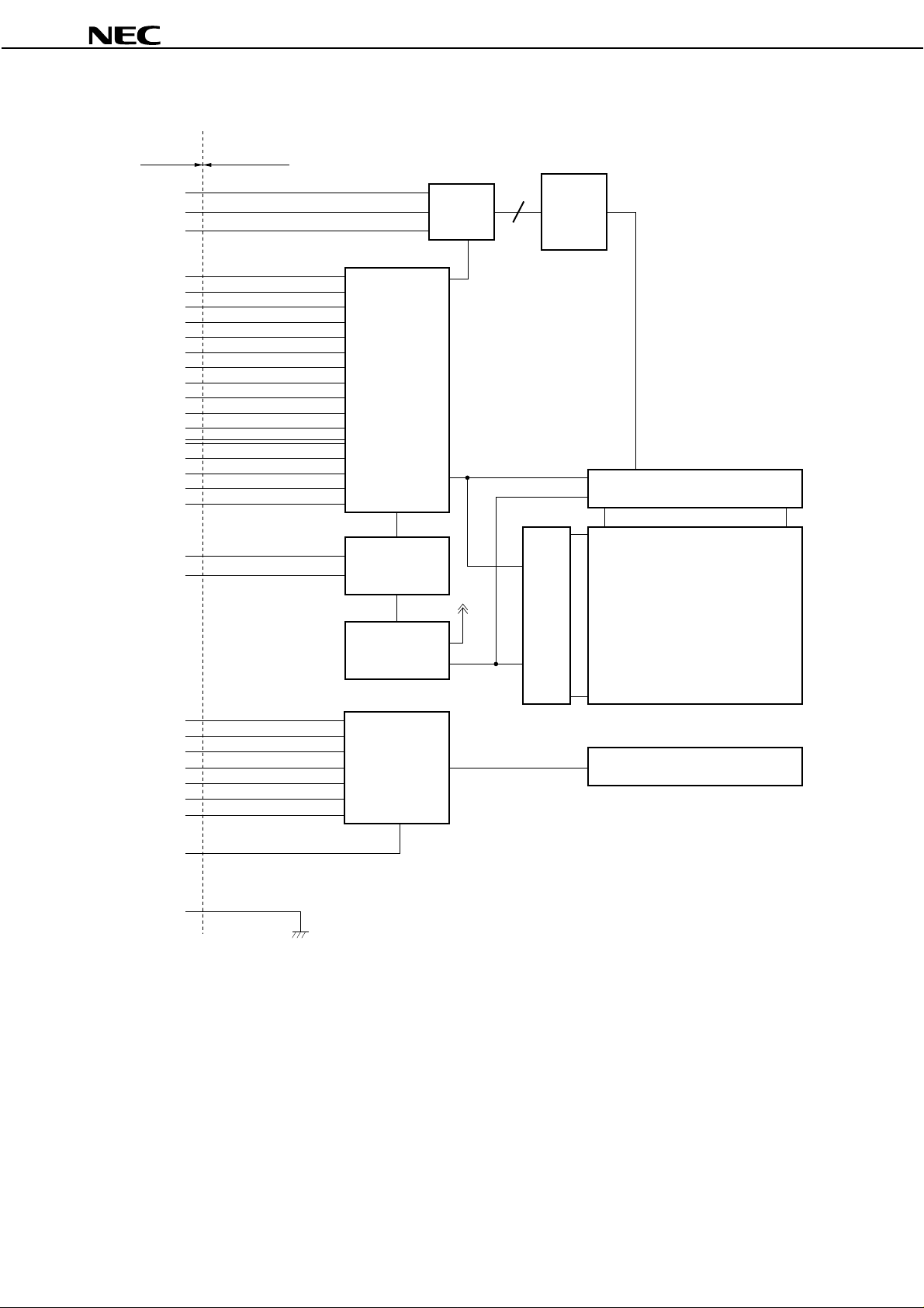
BLOCK DIAGRAM
NL10276AC30-03
I/F
R
G
B
Hsync
Vsync
CLK
DESEL
CLAMP
CPSEL
CNTDAT
CNTCLK
CNTSTB
CNTSEL
OSDENI
OSDRI
OSDGI
OSDBI
ADJSEL
CNTSTB2
POWC
VDD
LCD module
Timing controller
ON/OFF
AIF
V-driver
AMP
H-driver
3072 lines
LCD panel
768 lines
V
DD
B
BRTC
BRTH
BRTL
ACA
BRTP
PWSEL
GNDB
GND
Frame is not connected to GND and GNDB.
Note
DC/DC
converter
Inverter
HV: 1024 × 3 (R, G, B)
: 768
Backlight
Data Sheet EN0416EJ1V0DS00
3
Page 4

NL10276AC30-03
SPECIFICATIONS
GENERAL SPECIFICATIONS
Item Contents Unit
Module size 350.0 ± 0.6 (H) × 265.0 ± 0.6 (V) × 20.5 (max.) (D) mm
Display area 304.128 (H) × 228.096 (V) mm
Number of dots 1024 × 3 (H) × 768 (V) dots
Pixel pitch 0.297 (H) × 0.297 (V) mm
Dot pitch 0.099 (H) × 0.297 (V) mm
Pixel arrangement RGB (Red, Green, Blue) vertical stripe –
Display colors Full color color
Weight 1500 (max.) g
ABSOLUTE MAXIMUM RATINGS
Parameter Symbol Rating Unit Remarks
DD
V
DD
B –0.3 to +14 V
V
Logic input voltage Vin1 –0.3 to +5.5 V
R, G, B input voltage Vin 2 –6.0 to +6.0 V
CLK input voltage Vin 3 –7.0 to +7.0 V
BRTL input voltage Vin 4 –0.3 to +1.5 V
Storage temp. Tst –20 to + 60 °C –
Operating temp. Top 0 to +50 °C
Humidity
(no condensation)
Absolute humidity shall not exceed Ta = 50°C,
Measured at the display area
Note
–0.3 to +14 VSupply voltage
≤
95% relative humidity Ta ≤ 40°C
≤
85% relative humidity 40 < Ta ≤ 50°C
85% relative humidity level.
Ta = 25°C
Ta = 25°C
DD
= 12 V
V
Module surface
Ta > 50°C
Note
4
Data Sheet EN0416EJ1V0DS00
Page 5

ELECTRICAL CHARACTERISTICS
(1) Logic, LCD driving, Backlight
Item Symbol Min. Typ. Max. Unit Remarks
DD
V
DD
B 11.4 12.0 12.6 V f or backlight
V
Logic input “L” voltage 1 V
Logic input “H” voltage 1 V
Logic input “L” voltage 2 V
Logic input “H” voltage 2 V
Input CLK voltage V
Input DC voltage level V
Logic input “L” current 1 I
Logic input “H” current 1 I
Logic input “L” current 2 I
Logic input “H” current 2 I
Logic input “L” current 3 I
Logic input “H” current 3 I
Logic input “L” current 4 I
Logic input “H” current 4 I
Logic input “L” current 5 I
Logic input “H” current 5 I
Supply current
IL1
IH1
IL2
IH2
ICLK
IDCCLK
IL1
IH1
IL2
IH2
IL3
IH3
IL4
IH4
IL5
IH5
DD
I
DD
B – 750 850 mA VDDB = 12.0 V
I
11.4 12.0 12.6 V for Logic and LCD drivingSupply voltage
0–0.6V
4.5 – 5.25 V
0–0.8V
2.2 – 5.25 V
0.6–1.0Vp-p
–4.5 – +4.5 V
–10 – –
– – 160
–1400 – –
––10
µ
A
µ
A
µ
A
µ
A
–1.0 – – mA
––0.8mA
–1.0 – – mA
––10mA
–10 – –
––10
µ
A
µ
A
– 550 800 mA
NL10276AC30-03
(Ta = 25°C)
for BRTP
Logic except BRTP
CLK
Hsync, Vsync
CNTSEL, CPSEL , POW C, ADJSEL
BRTC, BRTL, ACA, PWSEL
BRTP
Logic except inputs above
DD
V
= 12.0 V
(Max. luminance)
Note
Pixel checkered pattern
Note
(2) Video signal (R, G, B) input
Item Min. Typ. Max. Unit Remarks
Maximum amplitude (white - black) 0
DC input level (black)
(3) CLK input equivalent circuit
CLK
0.7
(black)
−
3.5 – +3.5 V –
(white)
0.9 Vp-p Contrast adjustment is needed if the
amplitude exceeds 0.7 Vp-p.
1000 pF
510 Ω
(Ta = 25°C)
Data Sheet EN0416EJ1V0DS00
5
Page 6

SUPPLY VOLTAGE SEQUENCE
(1) Sequence of power supply
Voltage
200 ms ≤
Synchronous signals, Control signals, CLK.
Note
CAUTION
Wrong power sequence may cause damage to the module.
Logic signals Note
POWC
V
30 ms ≤
NL10276AC30-03
DD
Time
0 ms <
0 ms <
a) Logic signals (synchronous signals and control signals) should be “0” voltage (V), when VDD is not input.
If higher than 0.3 V is input to signal lines, the internal circuit will be damaged.
b) LCD module will shut down the power supply of driving voltage to LCD panel internally when one of
CLK, Hsync, Vsync is not input more than 90 ms typically. As the display data are unstable in this
period, the display is disordered. But the backlight works correctly even in this period. So the backlight
ON/OFF should be controlled by BRTC signal.
c) The backlight ON/OFF (BRTC signal) should be controlled while logic signals are supplied. The
DD
backlight power supply (V
B) is not related to the power supply sequence. However, unstable data is
displayed when the backlight power is turned ON without logic signals.
DD
d) Keep POWC signal “L” more than 200 ms after the power supply (V
B) is input , if POWC signal is
controlled.
e) Analog RGB input are independent of this power supply sequence.
f) 12 V for backlight should be started up within 80 ms, otherwise the protection circuit makes the backlight
turn off.
6
Data Sheet EN0416EJ1V0DS00
Page 7

NL10276AC30-03
(2) Ripple of supply voltage
Please note that the ripple at the input connector of the module should be within the values shown in this table.
If the ripple is beyond these values, the noise may appear on the screen.
Acceptable range
The acceptable range of ripple voltage includes spike noise.
Note
DD
V
(for logic and LCD driver)
≤
100 mVp-p
DD
V
B
(for backlight)
≤
200 mVp-p
Examples of the power supply connection
a) Separate the power supply b) Put the filter
Power VDD
Power VDDB
Power
Filter VDD
Filter VDDB
(3) Inverter current wave
In the luminance control mode, the rush current below flows into the inverter of the module. The duty cycle
varies from 100% through 20% depending on the luminance control level. This might cause the noise on the
screen. Please evaluate the appropriate value of the capacitor in the filter to eliminate the noise.
Filter
Inverter circuit of NL10276AC30-03
Customer’s Power
supply
(12 V)
Rush current
GND
0 (A)
to V
DD
750 (mA)
Duty
Frequency*
* Frequency:
Vsync frequency × K*
* Vsync ≤ 75 Hz: K = 4.6
> 75 Hz: K = 3.6
Data Sheet EN0416EJ1V0DS00
7
Page 8
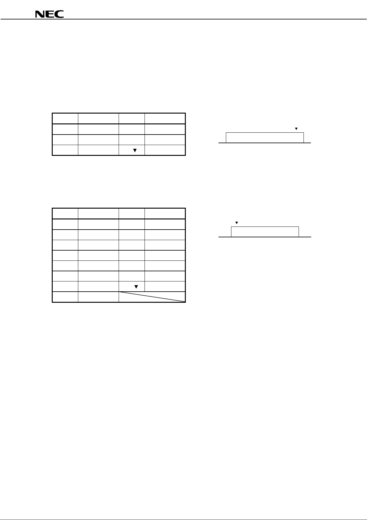
INTERFACE PIN CONNECTION
(1) CN1
Part No. : MRF03-6R-SMT
Adaptable socket: MRF03-6PR-SMT (board-to-board type)
MRF-03-6P-0.8D (cable type)
MRF-03-6P-1.27 (cable type)
Supplier : HIROSE ELECTRIC CO., LTD.
NL10276AC30-03
Pin No. Symbol Pin No. Symbol
1B4Vsync
2 G 5 Hsync
3R6CLK
(2) CN3
Part No. : IL-Z-15PL-SMTY
Adaptable socket: IL-Z-15S-S125C3
Supplier : Japan Aviation Electronics Industry Limited (JAE)
Pin No. Symbol Pin No. Symbol
1VDD9GND
2VDD10 CNTCLK
3 GND 11 CPSEL
4 GND 12 CLAMP
5POWC13GND
6 CNTSE L 14 N.C.
7 CNTDAT 15 GND
8 CNTSTB
Figure from socket view
······12 56
Figure from socket view
····15 14 12
N.C. (No connection) should be open.
Note
8
Data Sheet EN0416EJ1V0DS00
Page 9

(3) CN3
Part No. : DF14A-20P-1.25H
Adaptable socket: DF14-20S-1.25C
Supplier : HIROSE ELECTRIC CO., LTD
NL10276AC30-03
Pin No. Symbol Pin No. Symbol
1 GND 11 ADJSEL
2 OSDENI 12 N.C.
3 GND 13 CNTSTB2
4OSDBI14GND
5 GND 15 N.C.
6 OSDGI 16 GND
7 GND 17 N.C.
8 OSDRI 18 N.C.
9 GND 19 N.C.
10 N.C. 20 N.C.
N.C. (No connection) should be open.
Note
(4) CN201
Part No. : IL-Z-11PLI-SMTY
Adaptable socket: IL-Z-11S-S125C3
Supplier : Japan Aviation Electronics Industry Limited (JAE)
Figure from socket view
····12 2019
Pin No. Symbol Pin No. Symbol
1V
2V
3V
4 GNDB 10 BRTL
5 GNDB 11 N.C.
6 GNDB
DD
B7ACA
DD
B8BRTC
DD
B9BRTH
(5) CN202
Part No. : IL-Z-9PL1-SMTY
Adaptable socket: IL-Z-9S-S125C3
Supplier : Japan Aviation Electronics Industry Limited (JAE)
Pin No. Symbol Pin No. Symbol
1 GNDB 6 B RT L
2 GNDB 7 BRTP
3 A CA 8 GNDB
4BRTC9PWSEL
5BRTH
Figure from socket view
11 10
···· 12
Figure from socket view
···· 12
98
N.C. (No connection) should be open.
Note
Data Sheet EN0416EJ1V0DS00
9
Page 10
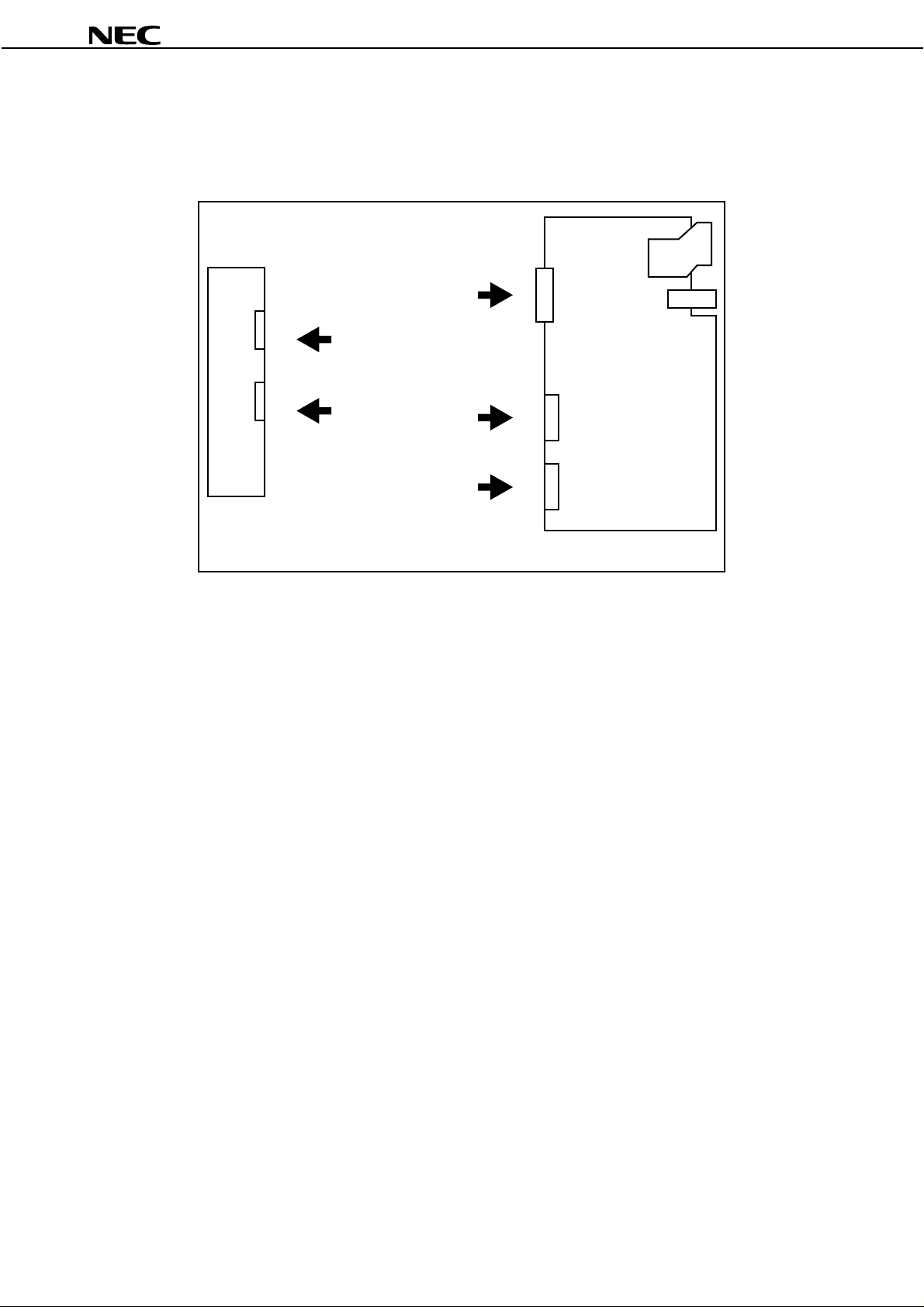
Caution For CN201 and CN202, pins with an identical symbol are connected inside the module.
<Rear view>
NL10276AC30-03
Do not use both of these pins at the same time.
1
11
CN202
1
9
CN201
1
CN1
6
15
CN3
1
1
CN4
20
10
Data Sheet EN0416EJ1V0DS00
Page 11

NL10276AC30-03
PIN FUNCTION
Symbol I/O Logic Description
CLK Input Positive Dot clock input . (ECL level ) This timing-signal is for display data.
Hsync I nput Negativ e Horizontal synchronous signal input (TTL level)
Vsync Input Negative Vertical synchronous signal input (TTL level)
R Input – Red video signal input (0.7 Vp-p, 75 Ω)
G Input – Green video signal input (0.7 Vp-p, 75 Ω)
B Input – Blue video signal input (0.7 Vp-p, 75 Ω)
POWC Input Positive Power control signal (TTL level)
“H” or “Open”: Logic and LCD power are on.
“L” : Logic and LCD power are off.
When POWC is “L”, serial communication data is cleared.
Please set again.
CNTSEL Input – Display control signal in case of serial communications. (TTL level)
“H” or “Open” : Default , “L” : External control
External control is set up by serial communication.
CNTDAT Input Positive Dis pl ay cont rol data (TTL level)
Detail of CNTDAT is mentioned in
CNTCLK Input Positive
CNTSTB Input Positive Lat ch pulse for display control data (TTL level)
CPSEL Input – CLAMP function select signal
CLAMP Input Negative Clamp timing signal of black level (TTL level)
ADJSEL Input Positive Contrast, brightness select control signal (TTL level)
CNTSTB2 Input P ositive Latch pulse2 for display control data
OSDRI Input – Input OSD-R data
OSDGI Input – Input OSD-G data
OSDBI Input – Input OSD-B data
OSDENI Input Positive Enable signal for OSD
CLK for display control data (TTL level)
Detail of CNTCLK is mentioned in
Detail of CNTSTB is mentioned in
“H” or “Open”: Default , “L” : External control
This mode works when CPSEL = “L”.
“H” or “Open”: Default , “L” : External control
Detail of CNTSTB2 is mentioned in
Detail is mentioned in
Detail is mentioned in
Detail is mentioned in
Detail is mentioned in
OSD FUNCTIONS
OSD FUNCTIONS
OSD FUNCTIONS
OSD FUNCTIONS
FUNCTIONS.
FUNCTIONS.
FUNCTIONS.
FUNCTIONS
(1/2)
Data Sheet EN0416EJ1V0DS00
11
Page 12
NL10276AC30-03
Symbol I/O Logic Description
ACA Input Positive Luminance control signal (TTL level)
“H” or “Open”: Normal luminance
“L” : Low luminance (1/2 of normal luminance)
BRTC Input Positive Backlight ON/OFF control signal (TTL level)
“H” or “Open”: Backlight ON, “L” : Backlight OFF
BRTH
BRTL
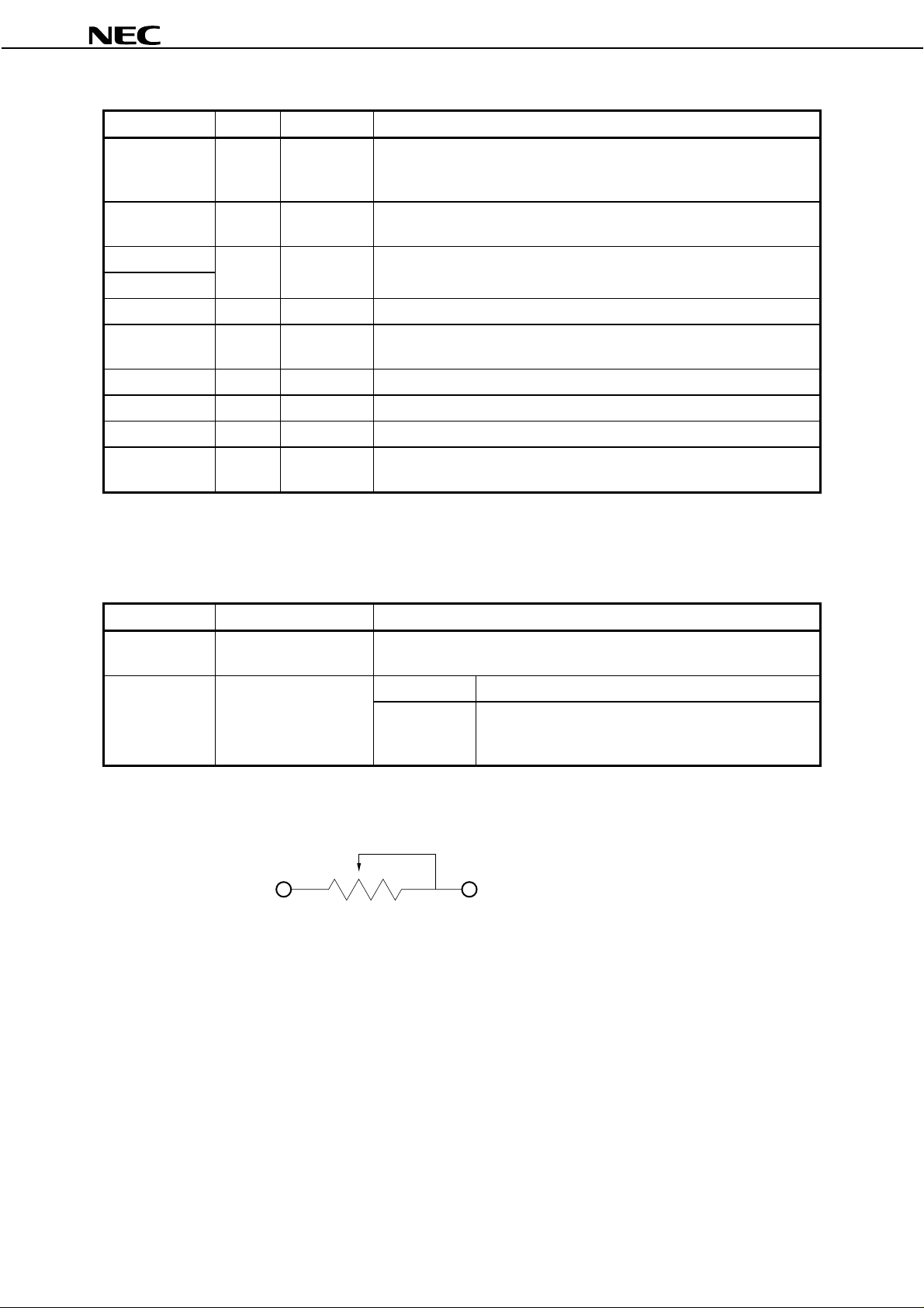
BRTP Input – Luminance control signal
PWSEL Input Positive
DD
V
VDDB – – Power supply for backlight. +12 V (±5 %)
GND – – Signal ground for Logic and LCD driving (Connect to system ground)
GNDB – – Ground for backlight, GNDB is not connected to the frame ground of LCD
Input – Variable resistor control of Voltage control
See [Function select] for detail.
Select the control of luminance (TTL level)
See [Function select] for detail.
– – Power supply for Logic and LCD driving +12 V (±5 %)
module.
(2/2)
Frame ground, system ground (GND) and backlight ground (GNDB) are not connected in the module.
Note
[Function select]
BRTP PWSEL How to adjust
Valid “L” Luminance can be controlled by BRTP signal.
See
OUTSIDE CONTROL FOR LUMINANCE
Open “H” or “Open”
The variable resistor for luminance control should be 10 kΩ type, and zero point of the resistor correspond
Note
Volume
Voltage
Please connect BRTP and BRTL.
Fix BRTH to “0 V” and input proper voltage to BRTL.
1 V: maximum luminance (100%)
0 V: minimum luminance (20%)
to the minimum of luminance.
Mating variable resistor:
BRTH BRTL
R
Maximum luminance (100 %)
Minimum luminance (20 %)
: R = 10 KΩ
: R = 0 Ω
10 KΩ ± 5 %, B curve
for more detail.
Note
12
Data Sheet EN0416EJ1V0DS00
Page 13
NL10276AC30-03
FUNCTIONS
This LCD module has following functions controled by serial data input (table 1)
(1) Control Display position (VERTICAL) : See table 3
(2) Control Display position (HORIZONTAL): See table 6
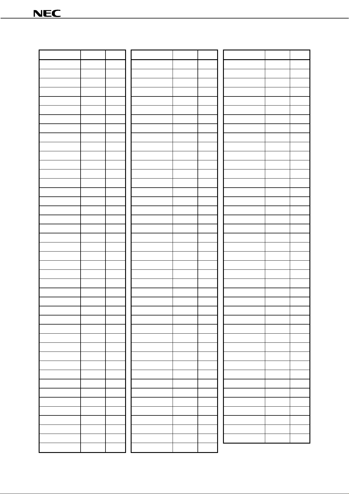
(3) Control CLK delay : See table 4
(4) Change CLK fall/rise synchronous : See table 5
(5) Contrast control :
(6) Sub-Contrast control :
(7) Sub-Brightness control :
Set up the following items to work the functions above
(A) Expansion mode : See table 2 and
(B) CLK counts of horizontal period : See table 7
(C) CLK frequency range : See table 8
HOW TO USE THE FUNCTIONS ABOVE
When CNTSEL is “L”, the functions ((1)-(4), (A)-(C)) above are valid. (When CNTSEL is “H” or open, default
values are valid.) After serial data are transferred, they are latched by CNTSTB. Once the data is latched, the
functions (1)-(4), (A)-(C) are effective.
See table 9, 10 and
GRAPH IMAGE
EXPANSION FUNCTION
COLOR CONTROL FUNCTION AND
When ADJSEL is “L”, functions (5)-(7) are valid. (When ADJSEL is “H” or open, default values are valid.)
After serial data are transferred, they are latched by CNTSTB2. Once the data is latched, the functions (5)-(7)
are effective.
Keep CNTSTB/CNTSTB2 “L” while transferring data.
Changing data is allowed when power is on. But display may be disturbed while changing. Turning off backlight
using BRTC function is recommended in this period.
Data Sheet EN0416EJ1V0DS00
13
Page 14
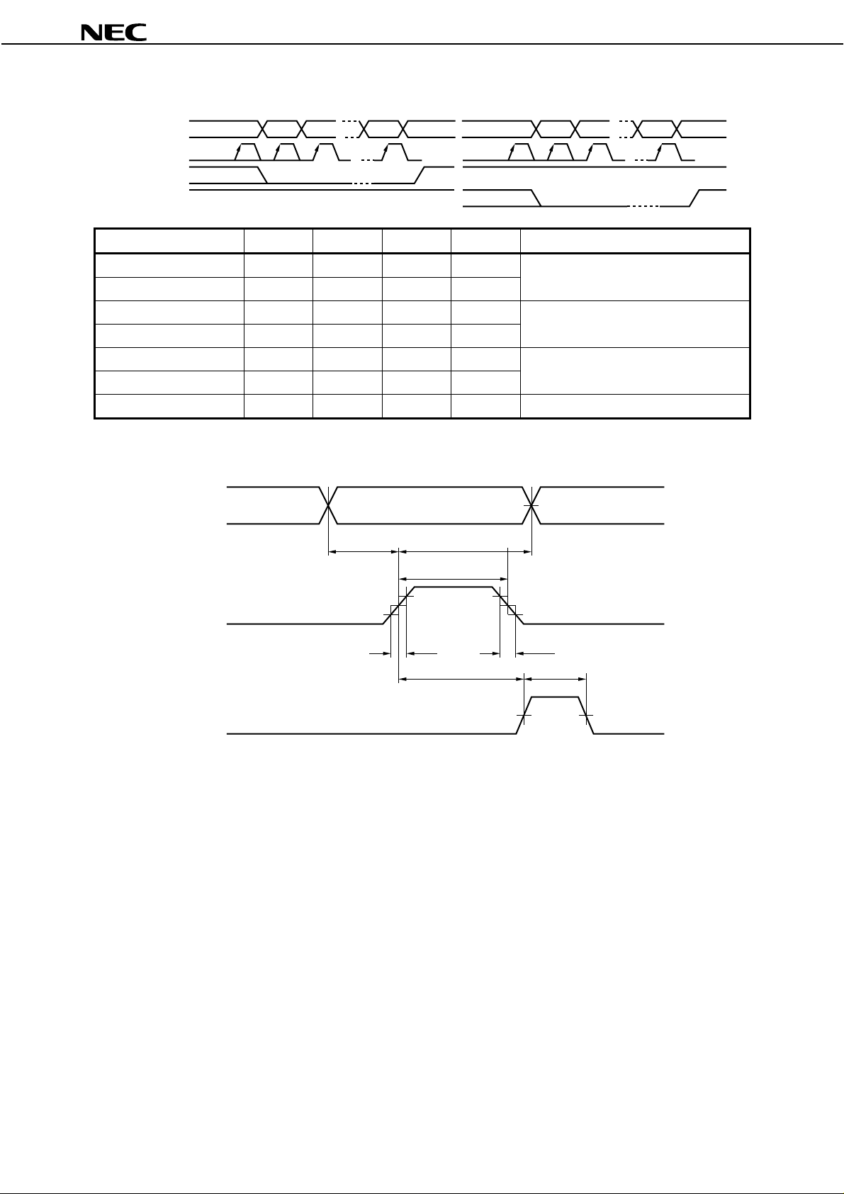
SERIAL COMMUNICATION TIMING AND WAVEFORM
NL10276AC30-03
CNTDAT
CNTCLK
CNTSTB
CNTSTB2
Parameter Symbol Min. Max. Unit Remark
CLK pulse-width Twck 50
CLK frequency Fclk
DATA set-up-time Tdst 50
DATA hold-time Tdhl 50
Latch pulse-width Twlp 50
Latch set-up-time Tlst 50
Rise / fall time Tr, Tf
D0 D1
D44 AD0 AD1 AD11INVALIDINVALID
−
−
−
5MHz
−
−
−
−
50 ns CNTXXX
ns
ns
ns
ns
ns
CNTCLK
CNTDAT
CNTSTB, CNTSTB2
SERIAL COMMUNICATION WAVEFORM
CNTDAT
Tdst Tdhl
50 %
VIH
VIL
CNTCLK
CNTSTB
CNTSTB2
Twch
50 %
10 %
Tr Tf
90 %
T1st Twlp
50 %
V
VIL
V
VIL
IH
IH
14
Data Sheet EN0416EJ1V0DS00
Page 15
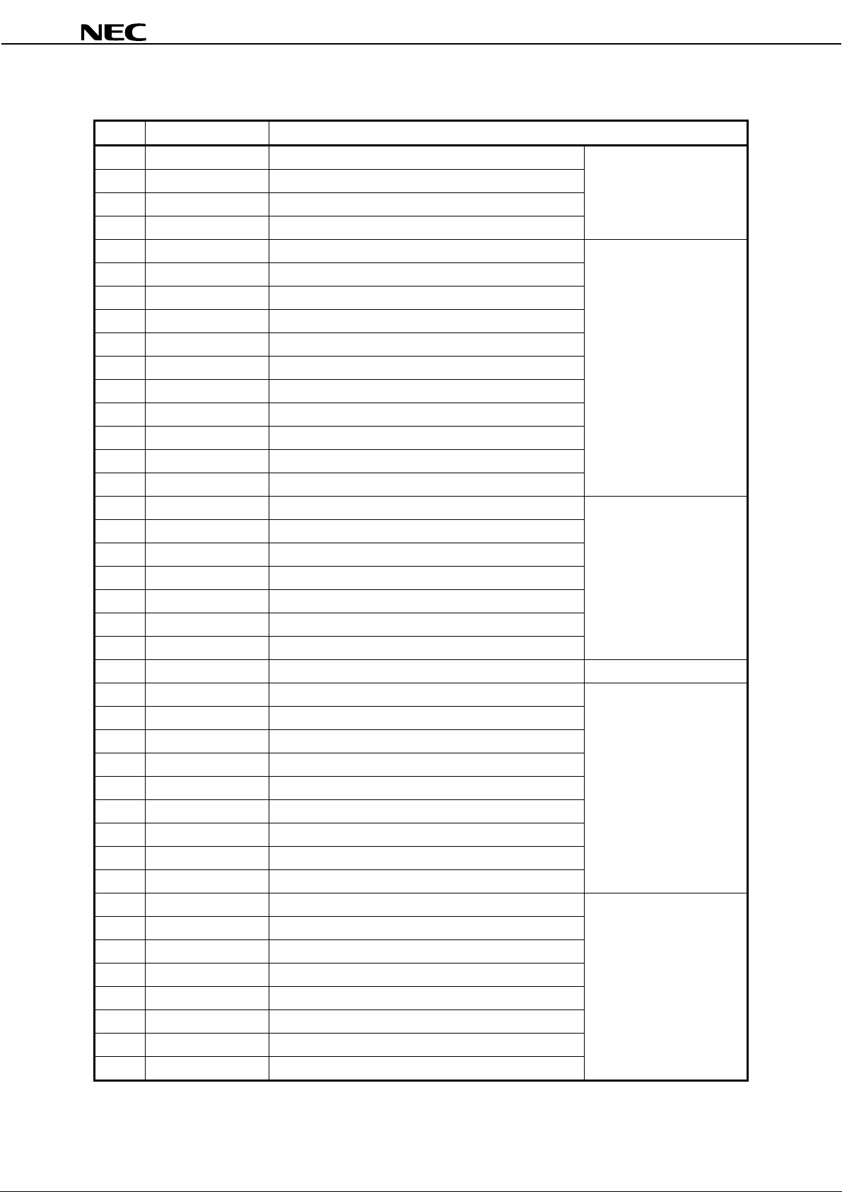
Table 1. CNTDAT Composition (1/2)
DATA DATA name Function
NL10276AC30-03
D0 VEX3 Expansion mode
D1 VEX2 Expansion mode
D2 VEX1 Expansion mode
D3 VEX0 Expansion mode
D4 VD10 Vertical display position (MSB)
D5 VD9 Vertical display position
D6 VD8 Vertical display position
D7 VD7 Vertical display position
D8 VD6 Vertical display position
D9 VD5 Vertical display position
D10 VD4 Vertical display position
D11 VD3 Vertical display position
D12 VD2 Vertical display position
D13 VD1 Vertical display position
D14 VD0 Vertical display position (LSB )
D15 DELAY6 CLK delay (MSB)
D16 DELAY5 CLK delay
D17 DELAY4 CLK delay
D18 DELAY3 CLK delay
D19 DELAY2 CLK delay
D20 DELAY1 CLK delay
D21 DELAY0 CLK delay (LSB)
D22 CKS CLK reverse signal See table 5
D23 HD8 Horizontal display position (MSB)
D24 HD7 Horizontal display position
D25 HD6 Horizontal display position
D26 HD5 Horizontal display position
D27 HD4 Horizontal display position
D28 HD3 Horizontal display position
D29 HD2 Horizontal display position
D30 HD1 Horizontal display position
D31 HD0 Horizontal display position (LSB)
D32 HS E 10 CLK count of horizontal period (MSB)
D33 HSE9 CLK count of horizontal period
D34 HSE8 CLK count of horizontal period
D35 HSE7 CLK count of horizontal period
D36 HSE6 CLK count of horizontal period
D37 HSE5 CLK count of horizontal period
D38 HSE4 CLK count of horizontal period
D39 HSE3 CLK count of horizontal period
See table 2
See table 3
See table 4
See table 6
See table 7
Data Sheet EN0416EJ1V0DS00
15
Page 16
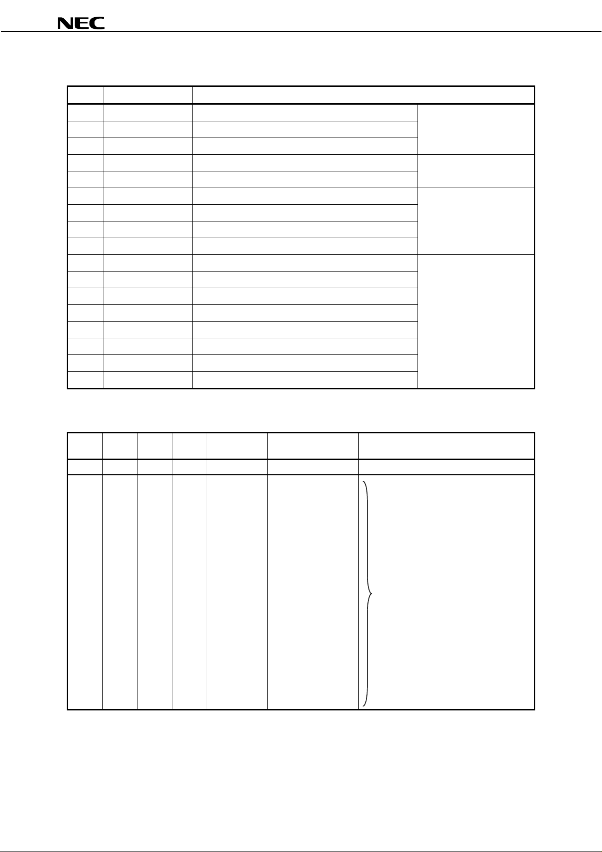
Table 1. CNTDAT Composition (continuation) (2/2)
DATA DATA name Function
NL10276AC30-03
D40 HSE2 CLK count of horizontal period
D41 HSE1 CLK count of horizontal period
D42 HSE0 CLK count of horizontal period (LSB)
D43 M OD1 CLK frequency select
D44 M OD0 CLK frequency select
AD11 DAA0 Color adjust select data (LSB)
AD10 DAA1 Color adjust select data
AD9 DAA2 Color adjust select data
AD8 DAA3 Color adjust select data (MSB)
AD7 DAD7 Color adjust data (MSB)
AD6 DAD6 Color adjust data
AD5 DAD5 Color adjust data
AD4 DAD4 Color adjust data
AD3 DAD3 Color adjust data
AD2 DAD2 Color adjust data
AD1 DAD1 Color adjust data
AD0 DAD0 Color adjust data (LSB)
See table 7
See table 8
See table 10
See table 9
Table 2. Display Mode (VEX3 to VEX0: 4 bit)
VEX3 VEX2 VEX1 VEX0
0 0 0 0 1 XGA S tandard
0 0 0 1 1.25 SVGA
0 0 1 0 1.6 PC98, VGA, TEXT
0 0 1 1 – Prohibit
0 1 0 0 – Prohibit
0 1 0 1 – Prohibit
0 1 1 0 – Prohibit
0 1 1 1 – Prohibit
1 0 0 0 – Prohibit
1 0 0 1 1.2 832 × 624 (MAC)
1 0 1 0 – Prohibit
1 0 1 1 – Prohibit
1 1 0 0 – Prohibit
1 1 0 1 – Prohibit
1 1 1 0 – Prohibit
1 1 1 1 – Prohibit
Vertical
magnification
Display mode Display image
See
Note
DISPLAY IMAGE
16
When CNTSEL is “H” or “Open”, display mode is fixed to XGA.
Note
Data Sheet EN0416EJ1V0DS00
Page 17
Table 3. Vertical Position (VD10 to VD0: 11 bit)
NL10276AC30-03
VD10 VD9 VD8 VD7 VD6 VD5 VD4 VD3 VD2 VD1 VD0
00000000000 Prohibit
00000000001 Prohibit
00000000010 Prohibit
00000000011 Prohibit
00000000100 4
00000000101 5
••••••••••• •
••••••••••• •
••••••••••• •
1 1 1 1 1 1 1 1 1 0 1 2045
1 1 1 1 1 1 1 1 1 1 0 2046
1 1 1 1 1 1 1 1 1 1 1 2047
Notes 1.
Horizontal line number for effective VIDEO signal from Vsync-fall is shown in this column.
The maximum vertical position is Vsync total.
2.
When CNTSEL is “H” or “Open”, vertical position is fixed to 35 [H].
3.
Vertical position [H]
Note 2
Note 1
Data Sheet EN0416EJ1V0DS00
17
Page 18
NL10276AC30-03
Table 4. CLK Delay (DELAY6 to DELAY0: 7 bit)
DELAY [6..0] Delay Unit DELAY [6..0] Delay Unit DELAY [ 6.. 0] Delay Unit
00H 9.5 ns 2BH 20.7 ns 56H 32.0 ns
01H 9.8 ns 2CH 20.9 ns 57H 32.2 ns
02H 10.0 ns 2DH 21. 2 ns 58H 32.6 ns
03H 10.3 ns 2EH 21.4 ns 59H 32.9 ns
04H 10.5 ns 2FH 21.7 ns 5AH 33.1 ns
05H 10.8 ns 30H 22.0 ns 5BH 33.4 ns
06H 11.0 ns 31H 22.2 ns 5CH 33.6 ns
07H 11.3 ns 32H 22.58 ns 5DH 33.8 ns
08H 11.5 ns 33H 22.8 ns 5EH 34.1 ns
09H 11.8 ns 34H 23.0 ns 5FH 34. 4 ns
0AH 12.1 ns 35H 23.3 ns 60H 34.7 ns
0BH 12.3 ns 36H 23.5 ns 61H 34.9 ns
0CH 12.5 ns 37H 23.8 ns 62H 35.2 ns
0DH 12.8 ns 38H 24.1 ns 63H 35.4 ns
0EH 13.1 ns 39H 24.3 ns 64H 35.7 ns
0FH 13.3 ns 3AH 24.6 ns 65H 36.0 ns
10H 13.6 ns 3BH 24.9 ns 66H 36.2 ns
11H 13.8 ns 3CH 25. 1 ns 67H 36.4 ns
12H 14.1 ns 3DH 25. 4 ns 68H 36.7 ns
13H 14.4 ns 3EH 25.6 ns 69H 37.0 ns
14H 14.6 ns 3FH 25.9 ns 6AH 37.3 ns
15H 14.9 ns 40H 26.2 ns 6BH 37.5 ns
16H 15.1 ns 41H 26.5 ns 6CH 37.7 ns
17H 15.4 ns 42H 26.7 ns 6DH 38.0 ns
18H 15.7 ns 43H 27.0 ns 6EH 38.2 ns
19H 16.0 ns 44H 27.2 ns 6FH 38. 5 ns
1AH 16.2 ns 45H 27.5 ns 70H 38.7 ns
1BH 16.5 ns 46H 27.7 ns 71H 39.0 ns
1CH 16.7 ns 47H 28.0 ns 72H 39.3 ns
1DH 17.0 ns 48H 28.3 ns 73H 39.5 ns
1EH 17.2 ns 49H 28.6 ns 74H 39.7 ns
1FH 17.5 ns 4AH 28.9 ns 75H 40.0 ns
20H 17.7 ns 4BH 29.1 ns 76H 40.3 ns
21H 18.0 ns 4CH 29. 4 ns 77H 40.5 ns
22H 18.3 ns 4DH 29. 6 ns 78H 40.8 ns
23H 18.5 ns 4EH 29.9 ns 79H 41.1 ns
24H 18.8 ns 4FH 30.1 ns 7AH 41.4 ns
25H 19.0 ns 50H 30.4 ns 7BH 41.6 ns
26H 19.3 ns 51H 30.7 ns 7CH 41.9 ns
27H 19.6 ns 52H 31.0 ns 7DH 42.1 ns
28H 19.9 ns 53H 31.2 ns 7EH 42.4 ns
29H 20.2 ns 54H 31.4 ns 7FH 42. 6 ns
2AH 20.4 ns 55H 31.7 ns
18
Data Sheet EN0416EJ1V0DS00
Page 19
NL10276AC30-03
Notes 1,
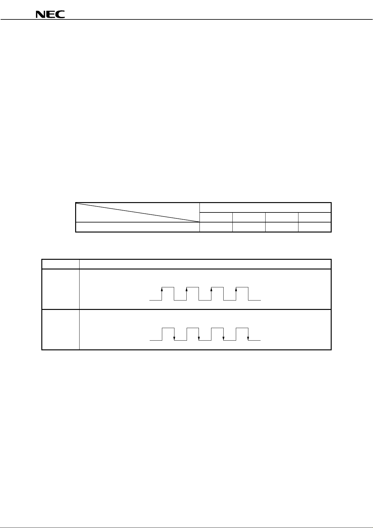
When CNTSEL is “H” or “Open”, DELAY[6..0] is fixed to 00H.
These values are typical at Ta = 25°C. Changing ambient temperature or power supply change the
2.
delay.
Please set up a preferable display position. See the following references.
<1> Variation of CLK delay by temperature drift (for reference). The temperature constant of CLK delay
is 0.2 %/°C.
Calculated example:
In case of delay time is 20 ns at Ta = 25°C;
(a) In case Ta rising to 50°C.
Increase of delay time → (50°C – 25°C) × 0.002 × 20 ns = +1 ns
So, the total delay time is 21 ns at Ta = 50°C.
(b) In case Ta falling to 0°C.
Decrease of delay time → (0°C – 25°C) × 0.002 × 20 ns = –1 ns
So, the total delay time is 19 ns at Ta = 0°C.
<2> Variation of CLK delay time between each LCD module (for reference).
–10.5 % to +14.4 %
MOD setting
0,0 0,1 1,0 1,1
The upper limit of CLK delay: DELAY [6..0] Prohibit 59H 6BH 7FH
Table 5. CLK Reverse Signal
CKS Function
0 DATA are sampled on rising edge of CLK
1 DATA are sampled on falling edge of CLK
When CNTSEL is “H” or “Open”, CKS is assumed to be “0”.
Note
Data Sheet EN0416EJ1V0DS00
19
Page 20
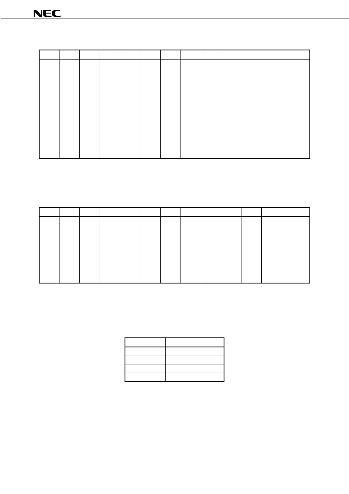
Table 6. Display Horizontal Position (HD8 to HD0: 9 bits)
NL10276AC30-03
HD8 HD7 HD6 HD5 HD4 HD3 HD2 HD1 HD0 Horizontal position [CLK]
000000000 Prohibit
000000001 Prohibit
••••••••• •
••••••••• •
000111111 Prohibit
001000000 64
001000001 65
••••••••• •
••••••••• •
111111101 509
111111110 510
111111111 511
Notes 1.
Number of CLKs from Hsync-fall to effective VIDEO signal is shown here.
When CNTSEL is “H” or “Open”, Horizontal position is set to 296 [CLK].
2.
Note 1
Table 7. CLK Count of Horizontal Period (HSE10 to HSE0: 11 bit)
HSE10 HSE 9 HSE 8 HSE 7 HSE 6 HSE 5 HSE 4 HSE 3 HSE 2 HSE 1 HSE 0 CLK count
00000000000 0
00000000001 1
••••••••••• •
••••••••••• •
••••••••••• •
1 1 1 1 1 1 1 1 1 0 1 2045
1 1 1 1 1 1 1 1 1 1 0 2046
1 1 1 1 1 1 1 1 1 1 1 2047
Note 1
Notes 1.
Notes 1.
Number of CLKs from Hsync to next Hsync.
When CNTSEL is “H” or “Open”, CLK count is set to 1344 [CLK].
2.
Selected CLK count must be identical with that of input signal.
3.
Table 8. CLK Frequency Select (MOD1 to MOD0: 2 bit)
MOD1 MOD0 CLK frequency [MHz]
0 0 Prohibit
0 1 65 to 80
1 0 50 to 65
1 1 20 to 50
Set up MOD1 and MOD0 complying with input CLK frequency.
When CNTSEL is “H” or “Open”, CLK frequency is set to 65 - 80 MHz.
2.
20
Data Sheet EN0416EJ1V0DS00
Page 21
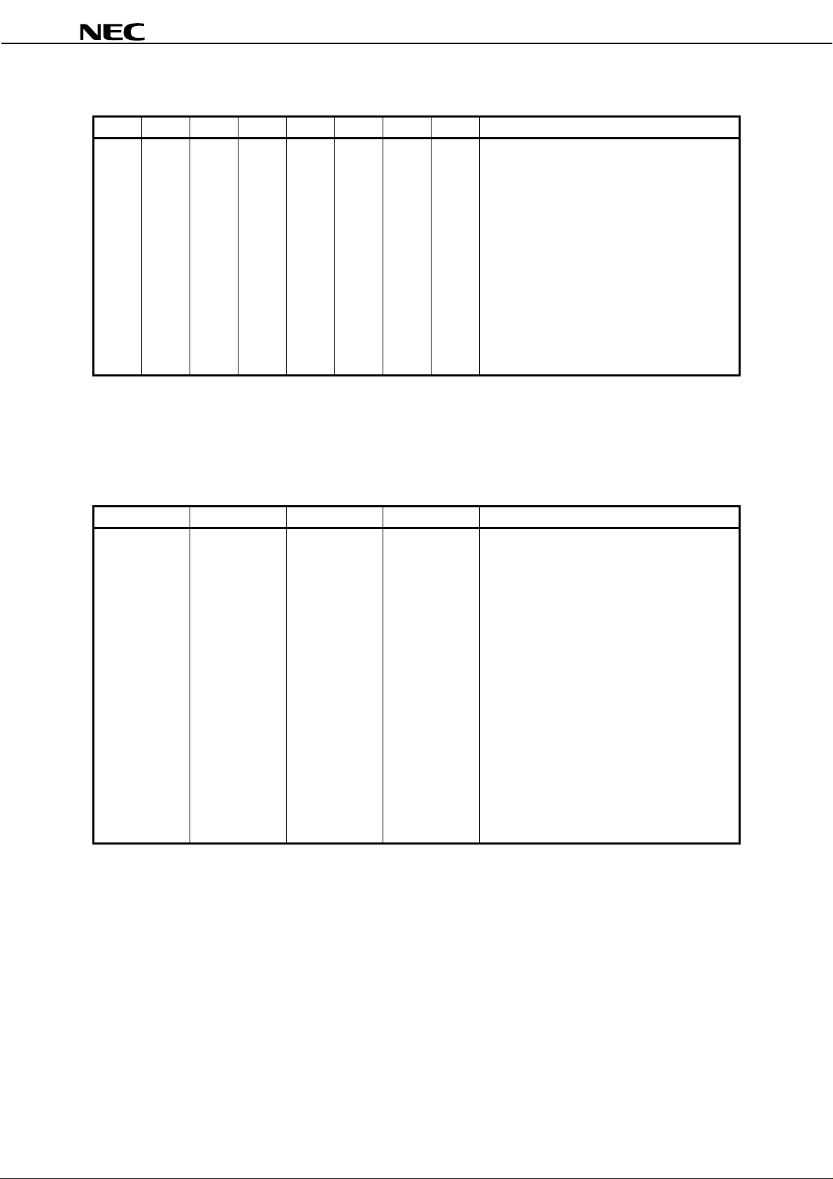
Table 9. Color Control Data (DAD7 to DAD0: 8 bit)
NL10276AC30-03
DAD7 DAD6 DAD5 DAD4 DAD3 DAD2 DAD1 DAD0 D/A
00000000 0
00000001 1
•••••••• •
•••••••• •
01111111 127
10000000 128
10000001 129
•••••••• •
•••••••• •
11111101 253
11111110 254
11111111 255
Notes 1.
Value for the function selected according to table 10.
Valid range of D/A depends on the selected function.
2.
See
3.
Color control function and graph image
for more detail.
Table 10. Color Adjust Select Data (DAA3 to DAA0: 4 bit)
DAA3 DAA2 DAA1 DAD0 Function
0 0 0 0 Prohibit
0001 Main contrast
0 0 1 0 Prohibit
0 0 1 1 Prohibit
0 1 0 0 Sub-contrast R
0 1 0 1 Sub-contrast G
0 1 1 0 Sub-contrast B
0 1 1 1 Sub-bri ghtness R
1 0 0 0 Sub-brightness G
1 0 0 1 Sub-brightness B
1 0 1 0 Prohibit
1 0 1 1 Prohibit
1 1 0 0 Prohibit
1 1 0 1 Prohibit
1 1 1 0 Prohibit
1 1 1 1 Prohibit
Note 1
See more de tail
Note
Color control function and graph image
Data Sheet EN0416EJ1V0DS00
.
21
Page 22
NL10276AC30-03
EXPANSION FUNCTION
HOW TO USE EXPANSION MODE
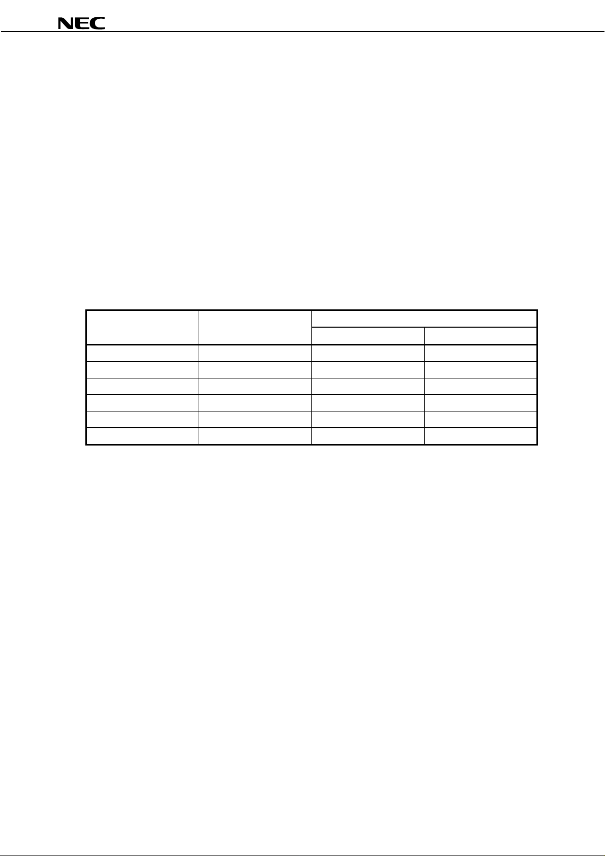
Expansion mode is a function to expand screen. For example, VGA signal has 640 × 480 pixels. But, if the
display data can expanded to 1.6 times vertically and horizontally, VGA screen image can be displayed fully on the
screen of XGA resolution.
This LCD module has the function of expanding vertical direction as shown in Table 1. And expanding horizontal
direction is possible by setting input CLK frequency which is equivalent to the magnification. It is necessary to make
this CLK outside of this LCD module.
The below image is display example, HD and VD is set to most suitable frequency.
Please adopt this mode after evaluating display quality, because the appearance of expansion mode is
happened to become bad some cases.
The followings show display magnifications for each mode.
Input display Num ber of pix els
XGA 1024 × 768 1 1
SVGA 800 × 600 1.25 1.25
VGA 640 × 480 1.6 1.6
VGA text 720 × 400 1.6 1.4
PC9801 640 × 400 1.6 1.6
MAC 832 × 624 1.2 1.2
The horizontal magnification multiples the input clock (CLK).
Note
Vertical
Magnification
Input CLK = system CLK × horizontal magnification
Example
In case of XGA and VGA, CLK frequency can be decided as follows.
XGA: (system CLK (65 MHz)) × 1.0 = 65 MHz
VGA: (system CLK (25.175 MHz)) × 1.6 = 40.28 MHz
Horizontal
Note
22
Data Sheet EN0416EJ1V0DS00
Page 23
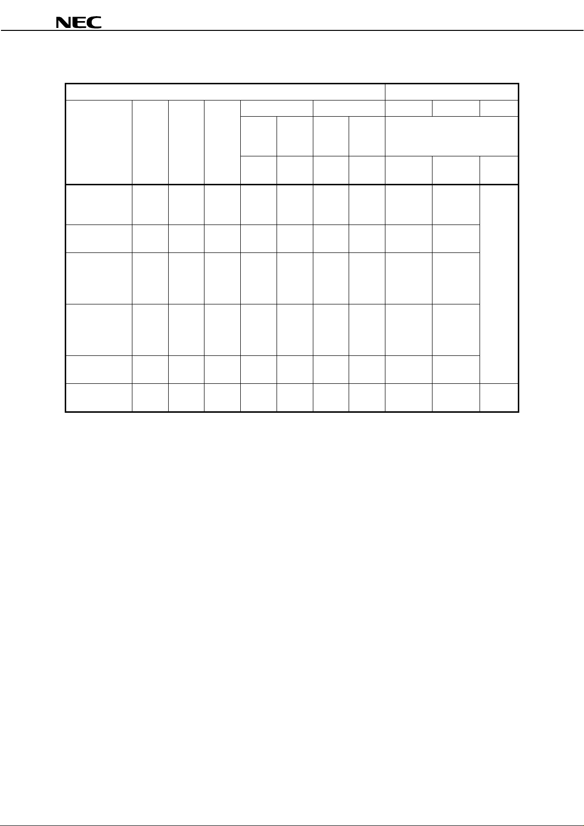
SETTING SERIAL DATA
System
Mode
CLK
[MHz]
Hsync
[kHz]
NL10276AC30-03
Input signal Module serial data setting
Horizontal Vertical HSE HD VD
Vsync
[Hz]
Count
Number
[CLK]
(A) (B)
DSP*
Note 1
[CLK]
Count
Number
[H]
−
DSP*
Note 1
[H]
(C)
Calculation formula
×
(A)
Ver.mag.
×
(B)
Hor.mag.
= (C)
XGA
(1024 × 768)
MAC
(832 × 624)
SVGA
(800 × 600)
VGA
(640 × 480)
VGA text
(720 × 400)
PC9801
(640 × 400)
Notes 1.
2.
3.
4.
5.
6.
65
48.363
75
56.476
78.75
57.283 49.725 74.5 1152 288 667 42 (A ) × 1.2 (B) × 1.2
36*
40*
50*
49.5*
25.175*
31.5*
31.5*
30.24*
28.322*
31.5*
21.053* 24.827 56.432 848 144 440 33 (A) × 1.6 (A) × 1.6 443
60.023
35.156
37.879
48.077
46.875
31.469
37.861
37.5
35.0
31.469
37.927
60.004
70.069
75.029
56.25
60.317
72.188
75
59.94
72.809
75
66.667
70.087
85.039
1344
1328
1312
1024
1056
1040
1056
800
832
840
864
900
936
296
280
272
200
216
184
240
144
168
184
160
153
180
806
806
800
625
628
666
666
525
520
500
525
449
446
35
35
31
24
27
29
24
35
31
19
42
37
45
(A) × 1(B)
(A) × 1.25 (B) × 1.25
(A) × 1.6 (B) × 1.6
(A) × 1.4 (B) × 1.4
×
= (C)
1
DSP = Display Start Period. DSP is total of “pulse-width” and “back-porch”.
HD and VD are approximate value. Set HD and VD in case of adjusting display to the screen center.
The pulse-width of Hsync, Vsync and back-porch are the same as XGA-mode. (Standard-mode).
HSE see CLK number of table 7.
HD see horizontal position of table 6.
VD see vertical position of table 3.
Data Sheet EN0416EJ1V0DS00
23
Page 24
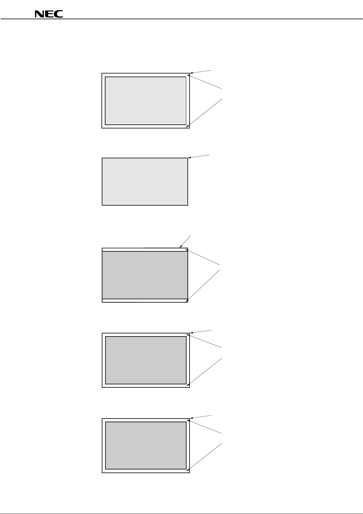
DISPLAY IMAGE
NL10276AC30-03
1) SVGA mode (800
2) VGA mode (640
××××
480)
3) PC9801 mode (640
××××
600)
××××
400)
XGA (1024 × 768)
Black display area
Horizontal
Vertical
XGA (1024 × 768)
Horizontal
Vertical
XGA (1024 × 768)
: × 1.25 (1000 pixels)
: × 1.25 (750 pixels)
: × 1.6 (1024 pixels)
: × 1.6 (768 pixels)
4) VGA text mode (720
5) 832
××××
624 MAC mode (832
××××
400)
××××
624)
Black display area
Horizontal
Vertical
XGA (1024 × 768)
Horizontal
Vertical
XGA (1024 × 768)
: × 1.6 (1024 pixels)
: × 1.6 (640 pixels)
Black display area
: × 1.4 (1008 pixels)
: × 1.6 (640 pixels)
Black display area
24
Data Sheet EN0416EJ1V0DS00
Horizontal
Vertical
: × 1.2 (998 pixels)
: × 1.2 (748 pixels)
Page 25
NL10276AC30-03
COLOR CONTROL FUNCTION AND GRAPH IMAGE
This LCD module can adjust the following functions by serial data input (table.1)
(1) Main contrast:
(2) Sub-contrast R/G/B: See table 9, 10 and
(3) Sub-brightness R/G/B:
(1) Main contrast
This function adjusts R/G/B contrast at the same tim e. Contr ast con trol the am plitude of input video signal.
Default value : 128
Valid range : 78 to 198
Contrast minimum : 198
Contrast maximum : 78
ADJSEL = “H” or “Open”: Maincontrast = 128
(2) Sub-contrast R, G, B
Sub-contrast can be adjusted for each R/G/B. Contrast control the amplitude of input video signal.
Default value : 128
Valid range : 78 to 198
Contrast minimum : 78
Contrast maximum : 198
ADJSEL = “H” or “Open”: Sub-contrast R.G.B = 128
Color control function and graph image
(3) Sub-brightness R, G, B
Sub-brightness can be adjusted for each R/G/B. Brightness adjust the black level of input video signal.
Default value : 128
Valid range : 55 to 163
Brightness minimum : 55
Brightness maximum : 163
ADJSEL = “H” or “Open”: Sub-brightness R.G.B = 128
Notes 1.
Setting these values out of proper ranges may cause deterioration of LCD. Keep the values in valid
ranges.
Difference between each LCD module may be seen even if the values for the functions are the
2.
identical. Moreover, optical characteristics are affected by this function. A sufficient evaluation to
adopt this function is recommended.
Data Sheet EN0416EJ1V0DS00
25
Page 26
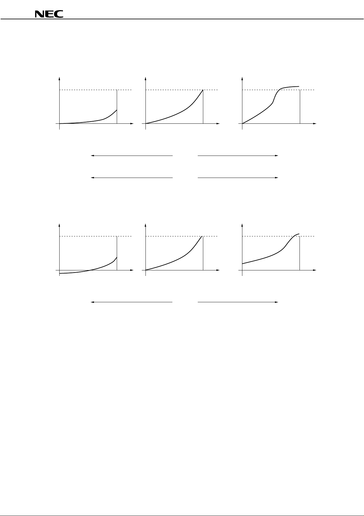
<GRAPH IMAGE>
Main contrast & Sub contrast
•
NL10276AC30-03
Relative
luminance
1
0
Black White
Gray scale
Main contrast
max. DEFAULT min.
Sub contrast
max. DEFAULT min.
Sub brightness
•
Relative
luminance
1
Relative
luminance
1
0
Black White
Gray scale
Relative
luminance
1
Relative
luminance
1
0
Black White
Gray scale
Relative
luminance
1
0
Black
Sub brightness
min. DEFAULT max.
Gray scale
White
0
Black White
Gray scale
0
Black White
Gray scale
26
Data Sheet EN0416EJ1V0DS00
Page 27
NL10276AC30-03
OSD FUNCTION
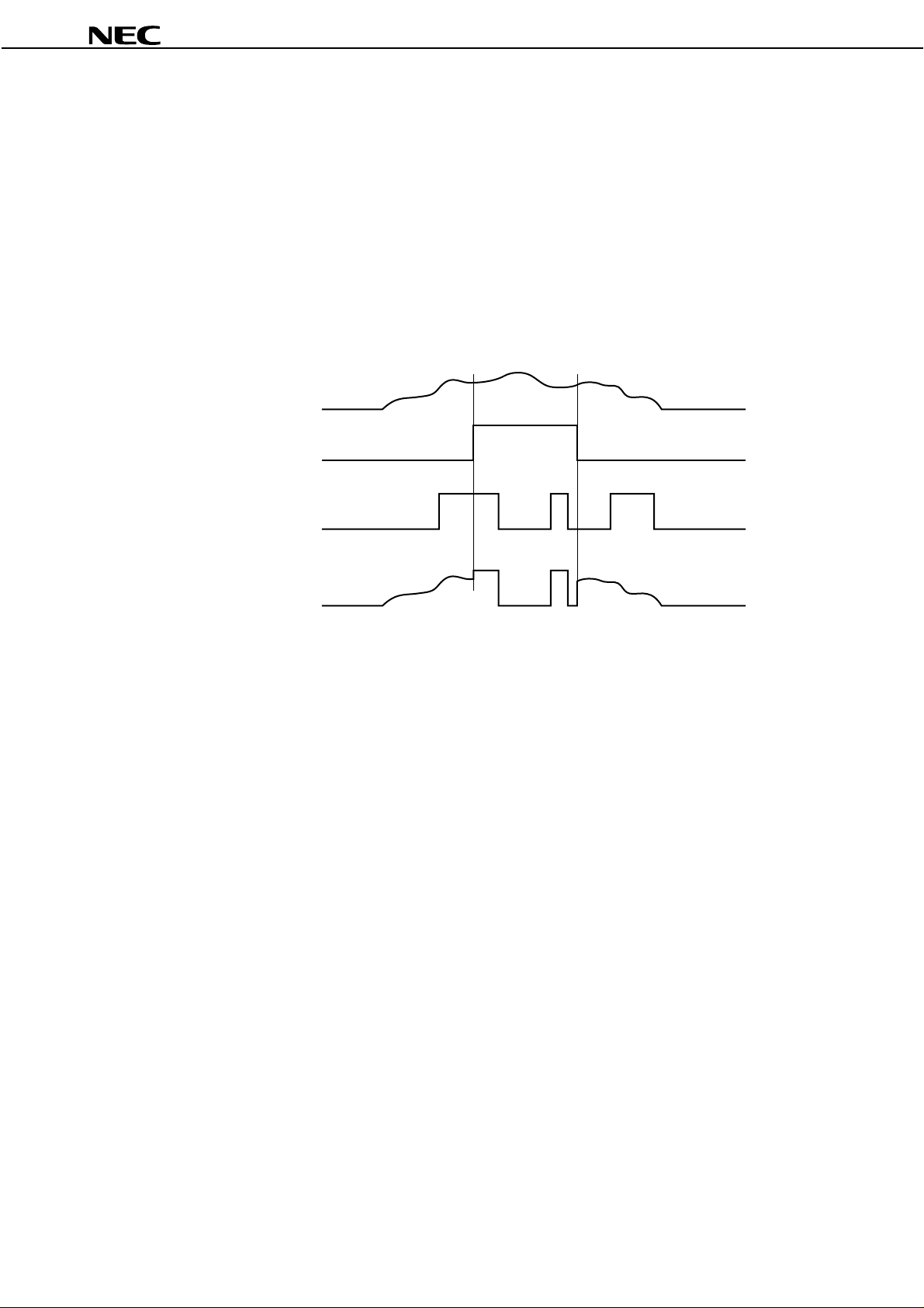
OSD (On Screen Display) is a function to display other digital data on analog data. Possible to display 1 bit data
for each R/G/B color (8 colors). OSD is valid for the period of OSDENI.
OSDRI, OSDGI, OSDBI: digital data for OSD
OSDENI = “H” : OSD signal is valid
OSDENI = “L” : OSD si gnal is not valid
OSD is a sub-display for function-control and the display quality is not guaranteed. Please adopt the OSD image
under sufficient evaluation of display quality.
<OSD image>
Analog R, G, B
OSDENI
OSDRI, GI, BI
Real display image
Regarding the use of OSD, please note that there is possibility of conflicts with a patent in Europe and the
Note
U.S.
Thus, if such conflict might happen when you use OSD, we shall not be responsible for any trouble.
Data Sheet EN0416EJ1V0DS00
27
Page 28
NL10276AC30-03
OUTSIDE CONTROL FOR LUMINANCE
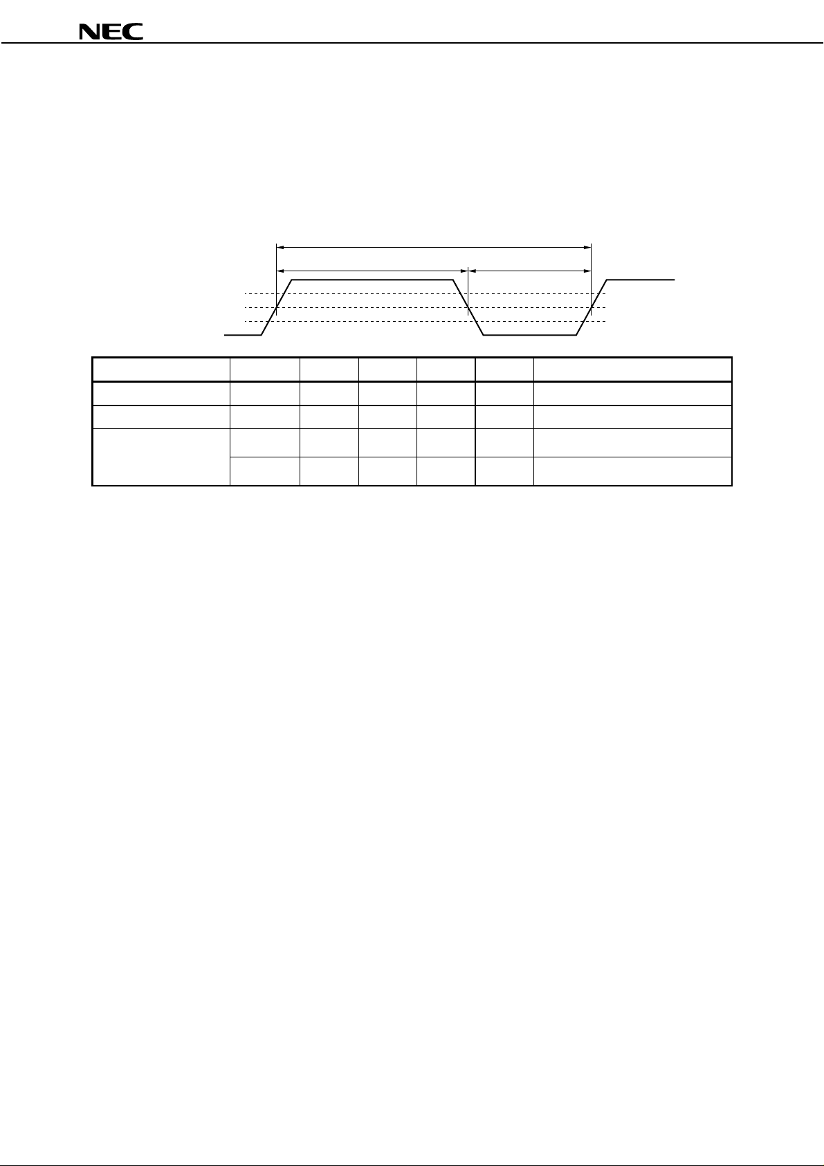
Outside control is valid when PWSEL = “L” and BRTP signal is inputted. Luminance can be controlled by the
duty value of input signal for BRTP.
Duty = 100%: Luminance is maximum.
Duty = 20% : Luminance is minimum.
Timing for BRTP
tPW
tHPW tLPW
V
IH
BRTP
Parameter Symbol Min. Typ. Max. Unit Remark
Frequency 1/tPW 185 – 340 Hz –
Pulse-width tHPW/tPW 20 – 100 % at max. luminance (100%)
Input voltage
50 %
V
IL
IL
V
IH
V
––0.6V
4.5 – – V
–
–
Regarding set up for the frequency, please refer to following method.
Set up the frequency = Vsync frequency × (n + 0.25) or (n + 0.75)
Please adopt the frequency under sufficient evaluation of display quality because the display may be disturbed
depending on a frequency.
28
Data Sheet EN0416EJ1V0DS00
Page 29
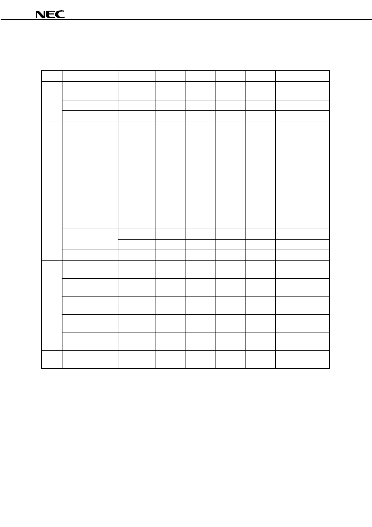
INPUT SIRIAL TIMING
XGA MODE (STANDARD)
Name Symbol Min. Typ. Max. Unit Remark
NL10276AC30-03
CLK
Hsync
Vsync
Analog
R, G, B
Frequency 1/tc 52.0
–
Rise/Fall tcrf – – 10 ns –
Pulse-width tcl/tc 0.4 0.5 0.6 – –
Period th 16.0
–
Display thd –
–
Front-porch thf
Pulse-width thp –
Back-porch thb 1.0
Pulse-width
+ Back-porch
Rise/Fall thrf – – 10 ns –
Period tv 13.3
Display tvd –
Front-porch tvf –
Pulse-width tvp –
Back-porch tvb –
– tda 4 – – ns –
thbp 1.8 – –
thvh3––CLK –Vsync - Hsync timing
thvs1––CLK –
–
10
16
44
–
–
1
2
5
65.0
15.385
20.677
1344
15.754
1024
0.369
24
2.092
136
2.462
160
16.665
806
15.880
768
62.031
3
124.06
6
599.63
29
80.0
–
22.7
–
–
–
–
–
–
–
–
–
18.5
–
–
–
–
–
–
–
–
–
MHz
ns
µ
s
CLK
µ
s
CLK
µ
s
CLK
µ
s
CLK
µ
s
CLK
µ
s–
ms
H
µ
s
H
µ
s
H
µ
s
H
µ
s
H
XGA standard
48.363 kHz (typ.)
Note
60.004 Hz (typ.)
–
–
–
–
–
–
–
Back-porch (thb) must exceed both 1.0
Note
s and 44 CLK.
µ
Data Sheet EN0416EJ1V0DS00
29
Page 30
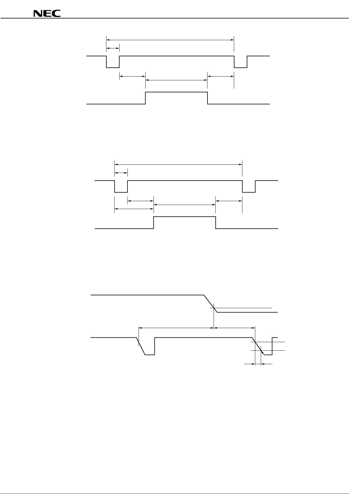
Vsync
NL10276AC30-03
tv
tvp
Display period
Hsync
Display period
tvb tvf
tvd
th
thp
thb thf
thd
thpb
30
Vsync
Hsync
thvh thvs
Data Sheet EN0416EJ1V0DS00
thrf
V
IL
V
IH
V
IL
Page 31
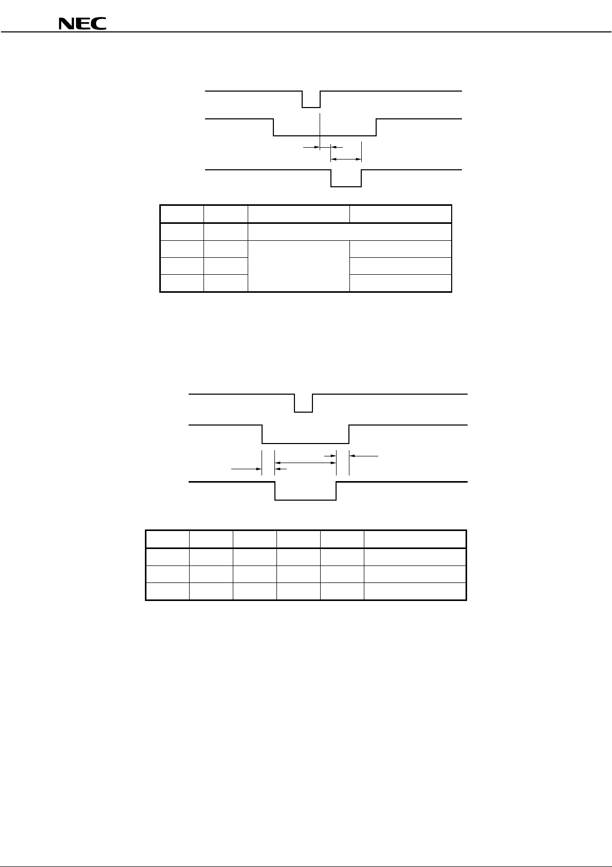
TIMING FOR GENERATING CLAMP SIGNAL INTERNALLY
Hsync
Display
period
NL10276AC30-03
tA
CLAMP
MOD1 MOD2 tA [CLK] tB [ns]
0 0 Prohibit
01 27
10 20
11
Exclude noises on analog R, G, B signal. Analog R, G, B signals are the black level reference during
Note
2
CLAMP = “L”. If noises are on the analog signals, luminance level of display is changed and the image
quality of the display may be worse.
TIMING FOR INPUTING CLAMP SIGNAL EXTERNALLY
Hsync
Display
period
tA
tB
tB
15
tC
CLAMP
Item Min. Typ. Max. Unit Remarks
tA 0.1
tB 0.3
tC 0.2
−−
−−
−−
µ
s
µ
s
µ
s
−
−
−
Note Exclude noises on analog R, G, B signal. Analog R, G, B signals are the black level reference during
CLAMP = “L”. If noises are on the analog signals, luminance level of display is changed and the image
quality of the display may be worse.
Data Sheet EN0416EJ1V0DS00
31
Page 32
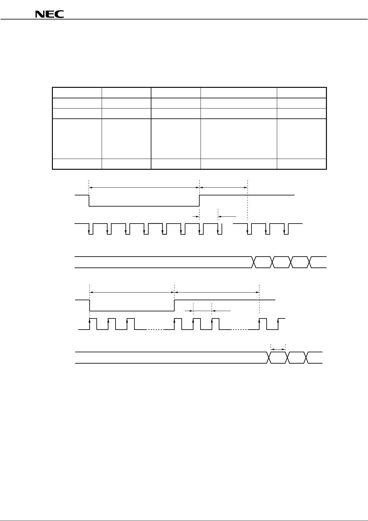
INPUT SIGNAL AND DISPLAY POSITION
XGA standard timing
Pixels
D (0, 0) D (0, 1) D (0, 2) • • • • • • D (0, 1023)
D (1, 0) D (1, 1) D (1, 2) • • • • • • D (1, 1023)
D (2, 0) D (2, 1) D (2, 2) • • • • • • D (2, 1023)
••• • •
••• • •
••• • •
••• • •
D (767, 0) D (767, 1) D (767, 2) • • • • • • D (767, 1023)
NL10276AC30-03
tvbtvp
Vsync
Hsync
XGA mode
(CNTSEL = “H” or “Open”)
R
G
B
Hsync
CLK
XGA mode
(CNTSEL = “H” or “Open”)
R
G
B
→
→
1 line
0123456 · · ·353637
Invalid Valid
thbthp
1 2 · · · 136 137 138
0 · · · 296 297
Invalid Valid
7
D(0,X) D(1,X) D(2,X)
1clk
tda
D(X,0) D(1,X) D(2,X)
32
tda should be minimum 4 ns.
Note
Data Sheet EN0416EJ1V0DS00
Page 33
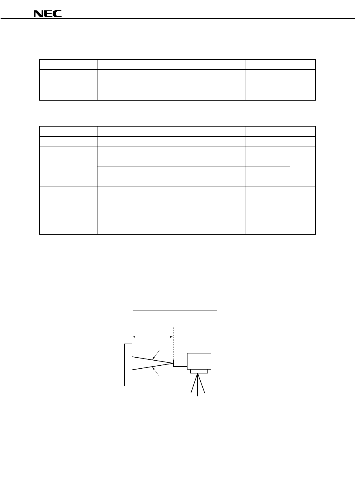
OPTICAL CHARACTERISTICS
NL10276AC30-03
(Ta = 25°C, V
Item Symbol Condition Min. Typ. Max. Unit Remark
Contrast ratio CR Perpendicul ar 80 200
Luminance Lvm ax White 150 200
Luminance uniformity
−
White
−−
Reference data
(Ta = 25°C, VDD = 12 V, VDDB = 12 V)
Item Symbol Condition Min. Typ. Max. Unit Remark
Contrast ratio CR Highest contrast ratio at θD = 10
θ
Viewing angle range
Color gamut C at center, to NTSC 35 42
Luminance
control range
Response time
R5055
θ
L
θ
U3550
θ
D
−
Ton white to black
Toff black to white
CR > 10,
CR > 10,
θ
U = 0°, θD = 0
θ
R = 0°, θL = 0
Maximum
luminance: 100%
°−
°
°
50 55
30 45
−
20 to 100
−
−
DD
= 12 V, VDDB = 12 V)
−−
−
cd/m
1.30
350
15 40 ms
40 50 ms
−−
−
−
−
−
−
−
deg.
deg.
deg.
deg.
Note 1
Note 2
2
−
Note 3
−
Note 1
Note 2
Note 4
%
%
−
−
Note 5
Note 5
Notes 1.
The luminance is measured at 20 minutes after power on, with all pixels in “white”. The typical value
is measured after luminance saturation.
Display mode : VESA XGA-75 Hz
RGB input voltage: 0.7 Vp-p
Contrast : Default value
The contrast ratio is calculated using the following formula.
2.
Contrast ratio (CR) =
LCD module
Luminance with all pixels in “white”
Luminance with all pixels in “black”
50 cm
Photo-detector (BM-5A)
1°
Data Sheet EN0416EJ1V0DS00
33
Page 34
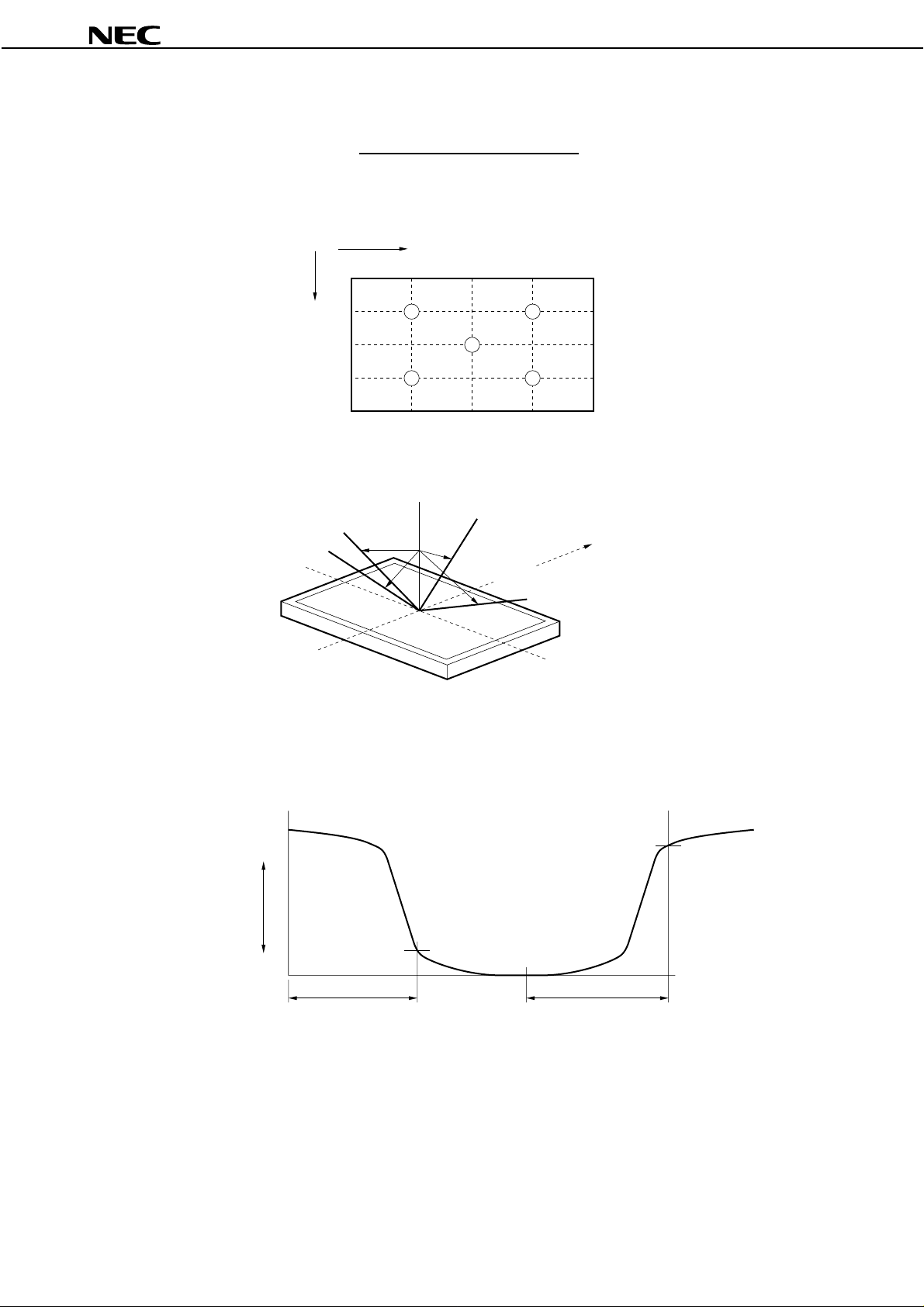
Luminance uniformity is calculated using the following formula.
3.
NL10276AC30-03
Luminance uniformity =
Maximum lumi nance
Minimum luminance
The luminance is measured near five points shown below.
Column
171 512 853
Row
3
4 5
Definitions of viewing angle are as follows.
4.
Normal
L
θ
–x
U
θ
R
θ
+y
21
128
384
640
12 o’clock
θ
D
–y
Definitions of response time is as follows.
5.
+x
Photo-detector output signal is measured when the luminance changes “white” to “black” and “black”
to “white”. Response time are Ton and Toff of the photo-detector output amplitude. Ton is the time
between 100% and 10%. Toff is the time between 0% and 90%.
100 %
Luminance
White
Black
10 %
0 %
Ton Toff
90 %
34
Data Sheet EN0416EJ1V0DS00
Page 35
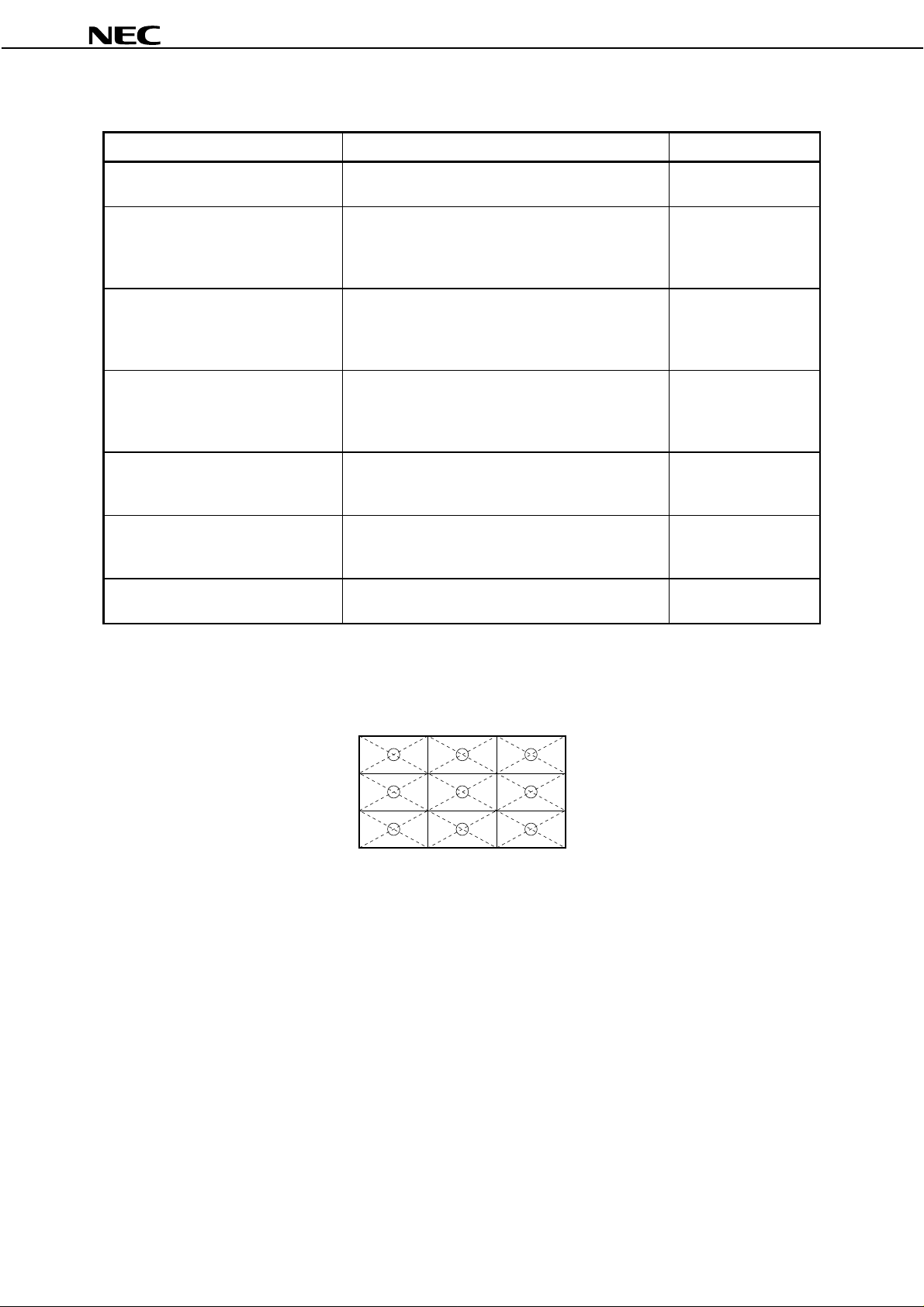
RELIABILITY TEST
Test item Test condition Judgment
NL10276AC30-03
High temperature/humidity operation 50 ±2°C, 85% relative humidity
240 hours, Display data is black.
Heat cycle (operation) <1> 0°C ±3°C ··· 1 hour
55°C ±3°C ··· 1 hour
<2> 50 cycles, 4 hours/cycle
<3> Display data is black.
Thermal shock (non-operation) <1>−20°C ±3°C ··· 30 minutes
60°C ±3°C ··· 30 minutes
<2> 100 cycles
<3> Temperature transition time is within 5 minut es.
Vibration (non-operation) <1> 5-100 Hz, 2 G
1 minute/cycle,
X, Y, Z direction
<2> 50 times each direction
Mechanical shock
(non-operation)
ESD (operation) 150 pF, 150 Ω, ±10 KV
Dust (operation) 15 kinds of dust (JIS Z 8901)
<1> 55 G, 11 ms
X, Y, Z direction
<2> 3 times each direction
9 places on a panel
10 times each place at one-second intervals
Hourly 15 seconds stir, 8 times repeat
Note 1
Note 1
Note 1
Notes 1, 2
Notes 1, 2
Note 1
Note 3
Note 1
Notes 1.
Display function is checked by the same condition as LCD module out-going in spection.
Physical damage.
2.
Discharge points are shown in the figure.
3.
Data Sheet EN0416EJ1V0DS00
35
Page 36
NL10276AC30-03
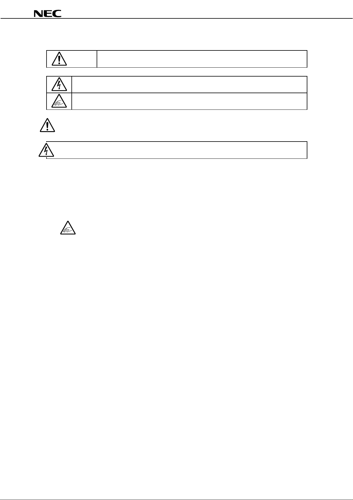
Next figures and sentences are very important. Please understand these, then read the text of a book.
This figure is a mark that you will get hurt and/or the module will have damages when you make
CAUTION
This figure is a mark that you will get an electric shock when you make a mistake to operate.
This figure is a mark that you will get hurt when you make a mistake to operate
CAUTION
Do not touch an inverter-on which is stuck a caution label-while LCD module is under operation, bec ause of
dangerous high voltage.
(1) Caution when taking out the module
<1> Pick the pouch only, in taking out module from a carrier box.
a mistake to operate.
(2) Caution for handling the module
<1> As the electrostatic discharges may break LCD modules, handle LCD modules with care against
electrostaic discharges.
<2> As LCD panels and backlight elements are made from fragile glass material, impulse and
pressure to LCD modules should be avoided.
<3> As the surface of polarizer is very soft and easily scratched, use soft dry cloth without chemicals for
cleaning.
<4> Do not pull the interface connectors in or out while LCD module is operating.
<5> Put modules display side down on a flat horizontal plane.
<6> Handle connectors and cables with care.
<7> The torque of mounting screw should be 0.392 N·m (4 kgf·cm) or less.
(3) Caution for the atmosphere
<1> Dew drop atmosphere should be avoided.
<2> Do not store and/or operate LCD modules in a high temperature and/or highly humid atmosphere.
Storage in an electro-conductive polymer packing pouch and under relatively low temperature atmosphere
is recommended.
<3> This module uses cold cathode fluorescent lamps. Therefore, the life time of lamps becomes short
conspicuously at low temperature.
<4> Do not operate LCD modules in a high magnetic field.
(4) Caution for the module characteristics
<1> Do not apply fixed pattern data signal to the LCD module at product aging. Applying fixed pattern for a
long time may cause image sticking.
(5) Other cautions
<1> Do not disassemble and/or reassemble LCD modules.
<2> Do not readjust variable resistor or switch etc.
<3> When returning modules for repair or etc., please pack the module not to be broken. We recommend the
original shipping packages.
36
Data Sheet EN0416EJ1V0DS00
Page 37
NL10276AC30-03
Liquid Crystal Display has the following specific characteristics. They are not defects or malfunctions.
The display conditions of LCD modules may be affected by the ambient temperature.
The LCD module uses cold cathode tubes for backlight. Optical characteristics, like luminance or
uniformity, will change during time.
Uneven brightness and/or small spots may be noticed depending on different display patterns.
Data Sheet EN0416EJ1V0DS00
37
Page 38
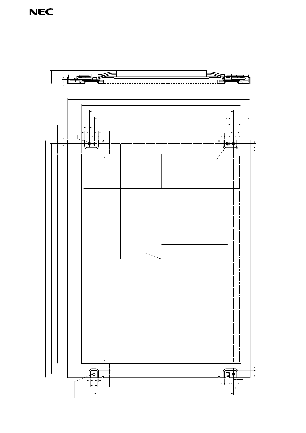
OUTLINE DRAWINGS
FRONT VIEW (Unit in mm)
4–3.4 ± 0.3
20.5 Max
NL10276AC30-03
± 0.3
15.6
4–2.7 ± 0.3
± 0.2
5
265 ± 0.6
232.7 ± 0.3 (BEZEL OPENING)
212 ± 0.3
197
18.6
5
± 0.3
2
3
φ
2
4
± 0.3
6
2
228.096 (ACTIVE AREA)
170 ± 0.7
97.8 ± 0.7
ACTIVE AREA CENTER
± 0.3
2 52
8–R4.4
5
±0.3
31 ± 0.3
6 ± 0.3
2
38
340 ± 0.3
350 ± 0.6
308.8 ± 0.3 (BEZEL OPENING)
φ
4– 3.5 ± 0.1
304.128 (ACTIVE AREA)
2
2 2
10 ± 0.3
6 ± 0.3
204 ± 0.3
Data Sheet EN0416EJ1V0DS00
2
5
2
8 ± 0.2
2
5±0.3
6 ± 0.3
· The torque to mounting screw should never exceed 0.392N · m (4 kg · cm)
· The tolerance of the dimensions that are not shown is ±0.5 mm.
Page 39
OUTLINE DRAWING (Unit in mm)
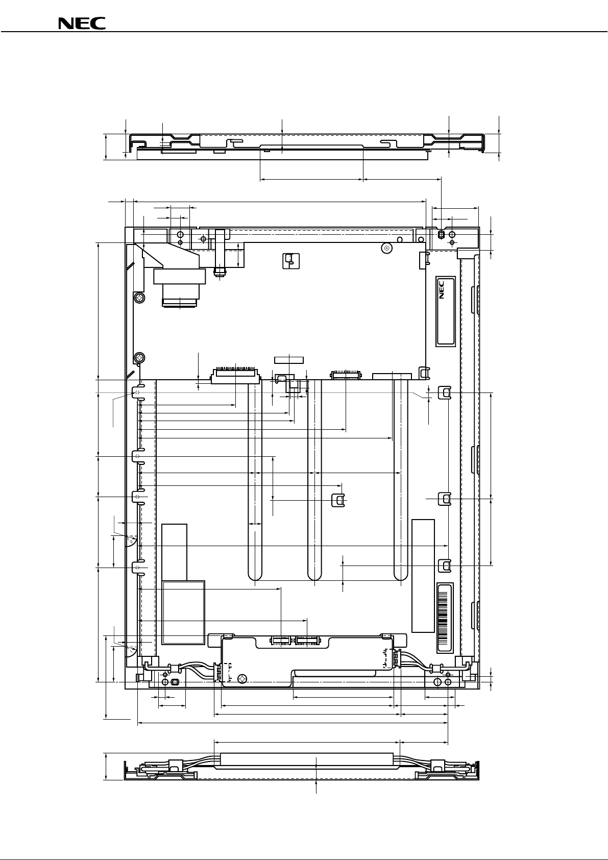
REAR VIEW
NL10276AC30-03
2.2
13.5
20.5 Max
5.5218
6.5
13.4
6.7
20.2
16
3.1 ± 0.2
9.4
71
111
M3BR (b)
115
7.6
MFR03-6R-SMT
CN1:
6
8.6
154 ± 1
189 ± 1
AMPSLIM-14P
CN2:
14 1
151
5
IL-Z-15P
CN3:
120
59 ± 1 78
DF14A-205
CN4:
0.4 ± 0.2
10.6
13.4
35.7
14.7
11.8
MADE IN JAPAN
· The tolerance of the dimensions that are not shown is ±0.5 mm.
NL10276AC30-03
804 53
54 ± 0.2 31 ± 0.2 48.6 ± 0.2 104.8
86.2 ± 0.2
62.8
85.765
45
152
32.5
8.7
10
231
23.8 ± 1
10.5
106.8 ± 1
Material Information
Light guide: >PMMA<
126.8 ± 1
R8 R8
THE TFT COLOR LCD
PANEL CONTAINS COLD CATHODE
FLOURESCEST LAMPS. PLEASE
FOLLOW LOCALORDINANCES
8.7
OR REGULATIONS FOR ITS
DISPOSAL
CN202CN201
11 1 9 1
A1000A763003
27 ± 1
5
76
20
22
40.7 ± 1 130
5
35.8 ± 1 139.8 ± 1
232.5
138
37 ± 1
20.5 Max
7.6
Data Sheet EN0416EJ1V0DS00
39
Page 40
NL10276AC30-03
DATA SHEET
No part of this document may be copied or reproduced in any form or by any means without the prior written
consent of NEC Corporation. NEC Corporation assumes no responsibility for any errors which may appear in this
document.
NEC Corporation does not assume any liability for infringement of patents, copyrights or other intellectual
property rights of third parties by or arising from use of a device described herein or any other liability arising
from use of such device. No license, either express, implied or otherwise, is granted under any patents,
copyrights or other intellectual property rights of NEC Corporation or others.
While NEC Corporation has been making continuous effort to enhance the reliability of its electronic components,
the possibility of defects cannot be eliminated entirely. To minimize risks of damage or injury to persons or
property arising from a defect in an NEC electronic component, customers must incorporate sufficient safety
measures in its design, such as redundancy, fire-containment, and anti-failure features.
NEC devices are classified into the following three quality grades:
"Standard", "Special", and "Specific". The Specific quality grade applies only to devices developed based on
a customer designated "quality assurance program" for a specific application. The recommended applications
of a device depend on its quality grade, as indicated below. Customers must check the quality grade of each
device before using it in a particular application.
Standard: Computers, office equipment, communications equipment, test and measurement equipment,
audio and visual equipment, home electronic appliances, machine tools, personal electronic
equipment and industrial robots
Special: Transportation equipment (automobiles, trains, ships, etc.), traffic control systems, anti-disaster
systems, anti-crime systems, safety equipment and medical equipment (not specifically designed
for life support)
Specific: Aircrafts, aerospace equipment, submersible repeaters, nuclear reactor control systems, life
support systems or medical equipment for life support, etc.
The quality grade of NEC devices is "Standard" unless otherwise specified in NEC's Data Sheets or Data Books.
If customers intend to use NEC devices for applications other than those specified for Standard quality grade,
they should contact an NEC sales representative in advance.
Anti-radioactive design is not implemented in this product.
 Loading...